
أفضل وحدات الكاميرات الحرارية UVC لأنظمة Linux و Pi والأنظمة المضمنة
٢١ يوليو ٢٠٢٦
أفضل وحدة كاميرا حرارية طويلة المدى لتكامل الذكاء الاصطناعي والطائرات بدون طيار: دليل OEM/ODM
٢٢ يوليو ٢٠٢٦
وحدة الكاميرا الحرارية بمستشعر CMOS: دليل التكامل وحلول OEM
إذا كنت قد قضيت أي وقت في الورشة في تصميم أنظمة المراقبة الآلية، أو بناء حمولات قوية للمركبات الجوية غير المأهولة (UAV)، أو تخطيط خطوط أتمتة المصانع المتقدمة، فأنت تعرف الوضع جيدًا. إن دمج كاميرا تصوير حراري مدمجة وموثوقة للغاية في هيكل ضيق يمثل تحديًا كبيرًا. في كثير من الأحيان، يبدأ مهندسو التصميم في البحث عن وحدة كاميرا حرارية بمستشعر CMOS على أمل محاكاة الأداء منخفض التكلفة وعالي السرعة لمصورات CMOS المرئية، ليواجهوا مباشرة جدارًا من أنماط الضوضاء والحدود البصرية وعدم توافق الواجهات.
في تصميم الأنظمة الإلكترونية البصرية الحديثة، فإن إيجاد النقطة المثلى بين الدقة، وتباعد البكسلات، وبروتوكولات الواجهة (مثل MIPI CSI-2، أو USB 3.0، أو CVBS، أو RJ45 RTSP)، وخطوط أنابيب المعالجة الحرارية هو ما يفصل بين جهاز ميداني من الطراز العالمي ونموذج أولي مهمل. إذا قمت بتوجيه خطوطك عالية السرعة بشكل غير صحيح، فستبدو صورتك الحرارية مثل شاشة تلفزيون مشوشة من عام 1985. وإذا اخترت طلاء العدسة الخاطئ، فسيتعرض كاشفك الحساس للعمى عند أول عاصفة قاسية في الميدان.
يتجاوز هذا المخطط الهندسي الزخارف التسويقية. سنشرح بالتفصيل كيفية عمل وحدات الكاميرا الحديثة غير المبردة بالأشعة تحت الحمراء طويلة الموجة (LWIR)، ونفحص الواجهات الفيزيائية والكهربائية التي ستتعامل معها على طاولة العمل، ونقدم وحدات OEM جاهزة للإنتاج صممتها Purpleriver. بدعم من فريق هندسي من الطراز العالمي يضم كفاءات من جامعة هونغ كونغ للعلوم والتكنولوجيا (HKUST) ومهندسي سيليكون سابقين من Huawei Hisilicon، تعمل هذه الوحدات كنقطة انطلاق موثوقة للغاية لنشر الأجهزة ذات المهام الحرجة.
جدول المحتويات
- 👉 التمييز التقني: مستشعر CMOS القياسي مقابل ROIC للميكروبولومتر
- 👉 الواجهات الفيزيائية والكهربائية لتكامل الأجهزة
- 👉 خطوط أنابيب المعالجة ASIC والمعايرة الحرارية
- 👉 كتالوج وحدات كاميرا المستشعر الحراري OEM من Purpleriver
- 👉 الهندسة البصرية واختيار العدسات لكاميرات LWIR
- 👉 الأسئلة الشائعة المتعمقة الشاملة (مرجع تقني)
التمييز التقني: مستشعر CMOS القياسي مقابل ROIC للميكروبولومتر
لنوضح أمرًا منذ البداية: من منظور فيزيائي، لا يوجد شيء اسمه "مستشعر CMOS مرئي قياسي" يقرأ الحرارة طويلة الموجة. عندما يشير العاملون في الصناعة إلى "وحدة كاميرا حرارية بمستشعر CMOS"، فإنهم في الواقع يتحدثون عن جهاز هجين شديد التعقيد. إنهم يقصدون مصفوفة كاشف حراري متخصصة من نوع الميكروبولومتر مبنية مباشرة فوق، ومتكاملة هيكليًا مع، دائرة متكاملة لقراءة CMOS (ROIC) دون الميكرون.
لفهم أهمية هذا التمييز على طاولة التكامل، ضع في اعتبارك الاختلافات الكهروضوئية. تعمل مستشعرات CMOS للضوء المرئي القياسية باستخدام التأثير الكهروضوئي ضمن النطاقات المرئية وتحت الحمراء القريبة (VNIR) (تقريبًا من 0.4 ميكرومتر إلى 1.0 ميكرومتر). تصطدم الفوتونات بمصفوفة ثنائي ضوئي من السيليكون النشط، مما يؤدي إلى قذف الإلكترونات إلى نطاق التوصيل لتوليد شحنة كهربائية تتوافق مباشرة مع السطوع البصري. السيليكون رخيص ومتوفر ويعمل بشكل جميل في هذه النطاقات.
ولكن عندما تعبر إلى طيف الأشعة تحت الحمراء طويلة الموجة (LWIR) - النطاق من 8 ميكرومتر إلى 14 ميكرومتر حيث توجد البصمات الحرارية الأرضية - يصبح السيليكون جدارًا منيعًا. إنه معتم تمامًا. لا يمكنك استخدام الثنائيات الضوئية القياسية لالتقاط هذه الأطوال الموجية. بدلاً من ذلك، تستخدم وحدات الكاميرا الحرارية ميكروبولومترات غير مبردة، مصنوعة عادةً من أكسيد الفاناديوم (VOx) أو السيليكون غير المتبلور (a-Si). إذا كنت تريد التعمق في الفيزياء الأساسية للإشعاع الحراري، فراجع التصوير بالأشعة تحت الحمراء في ويكيبيديا دليلنا.
هنا يحدث سحر CMOS فعليًا: كل بكسل جسر ميكروي فردي في مصفوفتك الحرارية معلق فيزيائيًا فوق رقاقة سيليكون CMOS أساسية. تعمل هذه الرقاقة كدائرة قراءة متكاملة (ROIC). الأرجل الهيكلية والميكانيكية للميكروبولومترات مثبتة على وسادات معدنية مستهدفة على شريحة السيليكون الأساسية تلك. عندما يصطدم الإشعاع الحراري الوارد بالغشاء المعلق، ترتفع درجة حرارته الفيزيائية، مما يغير مقاومته الكهربائية. تطبق دائرة القراءة المتكاملة (ROIC) بتقنية CMOS على المستوى الميكروي جهد انحياز دقيق للغاية ومنخفض للغاية عبر كل بكسل لقياس هذه التحولات الصغيرة في المقاومة، وتقوم بدمج وتجميع إشارات الجهد الخام في تدفق تناظري متماسك قبل تحويلها على الشريحة إلى خرج رقمي نظيف.
| معامل التشغيل | مستشعر CMOS للضوء المرئي القياسي | مستشعر LWIR الحراري (مع دائرة قراءة متكاملة CMOS) |
|---|---|---|
| النطاق الطيفي | 400 نانومتر – 1000 نانومتر (الضوء المرئي / الأشعة تحت الحمراء القريبة) | 8000 نانومتر – 14000 نانومتر (الأشعة تحت الحمراء طويلة الموجة) |
| آلية الاستشعار | توليد أزواج الإلكترونات والثقوب الكهروضوئية | تغير المقاومة البولومترية عبر الامتصاص الحراري |
| المادة الأساسية للمستشعر | سيليكون أحادي البلورة عالي النقاء | أكسيد الفاناديوم (VOx) أو السيليكون غير المتبلور (a-Si) |
| عناصر العدسة | زجاج بصري (سيليكا منصهرة، BK7) | الجرمانيوم (Ge)، زجاج الكالكوجينيد، السيليكون (Si) |
| إطار بيانات الخرج | نمط Bayer خام 8/10/12 بت | قيم راديومترية / عد رقمي خام 14 بت |
| بنية البكسل | مستشعر البكسل النشط (ترانزستور ضوئي 3T/4T) | ميكروبولومتر بجسر ميكروي معلق بتقنية MEMS فوق دائرة قراءة متكاملة |
الواجهات الفيزيائية والكهربائية لتكامل الأجهزة
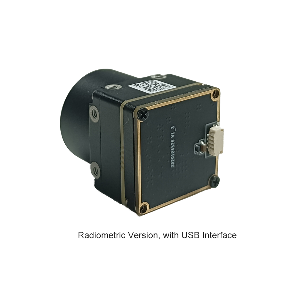
عندما تقوم بدمج إحدى هذه النوى في أجهزتك الفعلية، فإن اختيارك للواجهة الفيزيائية والكهربائية سيحدد نجاح أو فشل تصميمك. هذا الاختيار يضع القواعد لتخطيط لوحتك الفيزيائية، ويفرض استهلاكك للطاقة، ويتحكم في زمن انتقال خط الأنابيب. لا يوجد حل واحد يناسب الجميع هنا. يعتمد الأمر كليًا على ما إذا كانت وحدتك ستوضع في محور تثبيت طائرة بدون طيار عالية السرعة، أو أرضية مصنع مغبرة، أو غلاف مراقبة IP خارجي.
إليك كيفية تقييم الخيارات الرئيسية على منصة الهندسة:
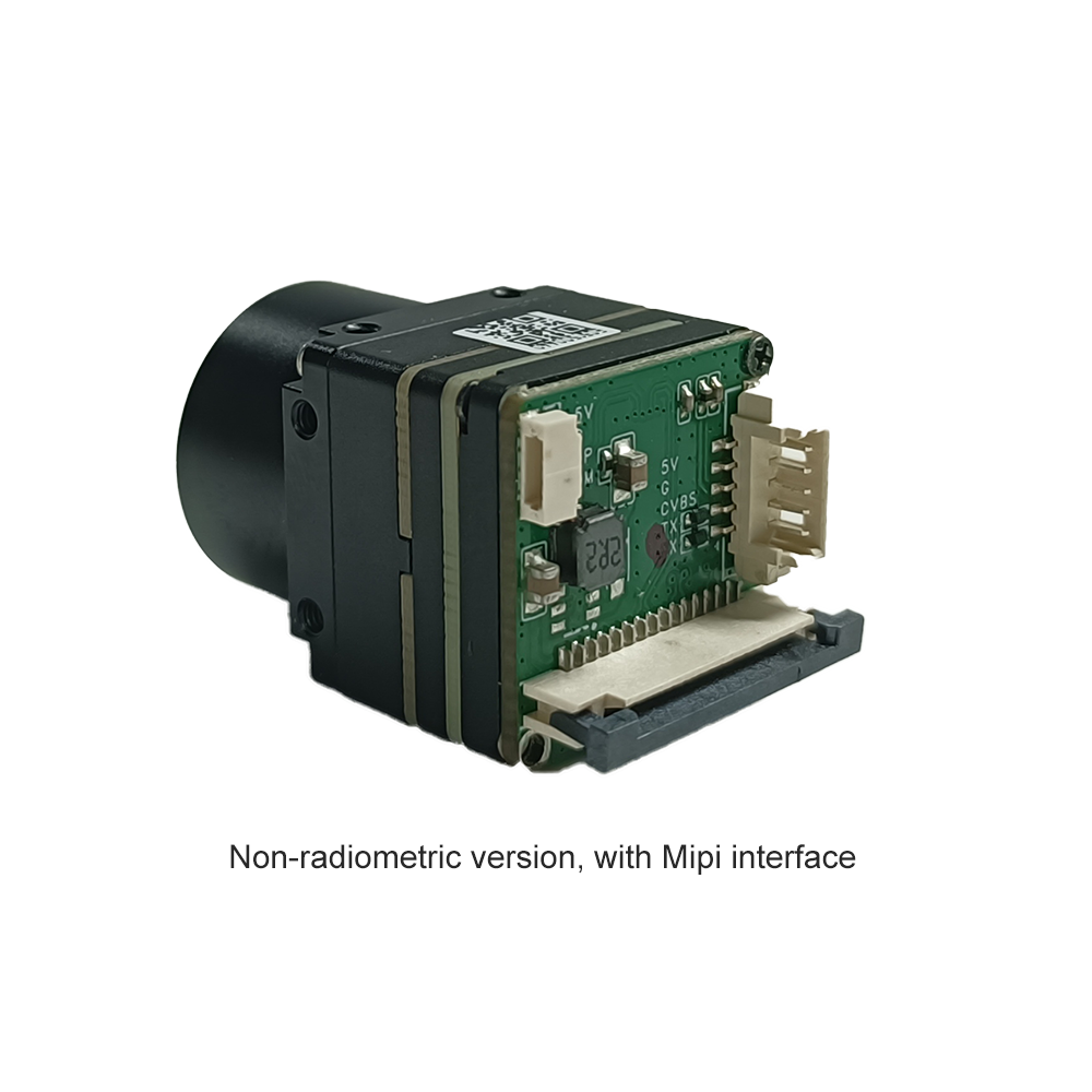
- 🔌 MIPI CSI-2 (واجهة معالج الصناعة المتنقلة): إذا كنت تبني أنظمة مدمجة بعمق تعمل على بنى نظام على شريحة (SoC) مثل NVIDIA Jetson Nano/Orin أو Rockchip أو Raspberry Pi، فإن MIPI CSI-2 هو أفضل صديق لك. يوفر هذا البروتوكول اتصالاً مباشرًا عالي النطاق الترددي بين الشرائح عبر مسارات فيزيائية تفاضلية (D-PHY). يرسل إطارات فيديو حرارية خام غير مضغوطة بدقة 14 بت بسرعة فائقة - عادة أقل من 5 ميلي ثانية من زمن انتقال الأجهزة. لكن انتبه: نظرًا لأن إشارات MIPI تعمل بترددات عالية، فإن تخطيط مسارات لوحة الدوائر المطبوعة (PCB) يتطلب تحكمًا صارمًا في المعاوقة التفاضلية، مستهدفًا 100 أوم بالضبط. إذا كنت توجه الإشارات عبر وصلة دوارة، مثل محور تثبيت طائرة بدون طيار، فاستخدم مجموعات كابلات ميكرو-محورية عالية المواصفات من موردين متخصصين مثل رجل الكابل المحوري الصغير للحفاظ على التداخل الكهرومغناطيسي (EMI) من إفساد تدفق البيانات الخاص بك.
- 💻 USB (الناقل التسلسلي العام): بالنسبة للنماذج الأولية التي تعمل بالتوصيل والتشغيل أو إعدادات سطح المكتب، فإن واجهات USB 2.0 أو USB 3.0 Type-C مريحة بشكل لا يصدق. باستخدام برامج تشغيل فئة فيديو USB القياسية (UVC)، تقدم وحدة الكاميرا الحرارية نفسها لنظام التشغيل لديك ككاميرا ويب أساسية. يمكنك سحب تدفق فيديو معالج بتنسيق 8-bit YUV أو MJPEG إلى تطبيقك على الفور دون الحاجة إلى تعديل نواة لينكس أو التعامل مع برامج تشغيل خاصة. والأفضل من ذلك، يمكن للوحدات ثنائية الوضع المتطورة تفريغ بيانات إشعاعية خام 14-bit عبر نقطة نهاية بديلة، مما يتيح لك إجراء حسابات درجة الحرارة لكل بكسل على جانب الجهاز المضيف.
- 📡 RJ45 Ethernet (تدفقات شبكة IP / RTSP): عندما تضطر إلى وضع عقدة مراقبة في أقصى نهاية ساحة صناعية، فإن Ethernet هو الخيار المنطقي الوحيد. تقوم معالجات ترميز الفيديو المدمجة بضغط إطارات الفيديو الخام ذات النطاق الترددي العالي إلى تدفقات مضغوطة عالية الكفاءة باستخدام برامج الترميز H.264 أو H.265. ثم يتم تقديم التغذية المضغوطة عبر RTSP (بروتوكول التدفق في الوقت الفعلي) أو ملفات تعريف ONVIF، لتتناسب بسلاسة مع شبكات الأمان الحالية. إذا كنت تنشر عقدًا محدودة الموارد الحاسوبية، ألق نظرة على كيفية استخدام البنى المدمجة لهذه الأنظمة على الحواسيب أحادية اللوحة من خلال مراجعة تحليلنا لـ thermal camera module for Raspberry Pi.
- 📺 CVBS (Composite Video Baseband Signal): Even in our digital-first world, legacy analog output (PAL or NTSC) is still a lifesaver. On commercial drone gimbals, FPV (First Person View) operators rely on single-coaxial analog RF transmitters because they degrade gracefully. If a digital link gets hit with interference, the screen freezes or goes black. With a CVBS link under heavy noise, you just get static—but you can still make out the horizon and save the drone from a costly crash.
خطوط أنابيب المعالجة ASIC والمعايرة الحرارية
Uncooled LWIR microbolometers are incredibly sensitive to their own internal temperature changes. If you attempt to display raw data straight out of the sensor, it looks like a noisy, non-uniform mess. Ambient heat from the camera's own processing chips, changing winds, or solar exposure on the casing causes the pixels to drift. To solve this, professional-grade modules run a dedicated ASIC processing pipeline that sits right behind the sensor. This ASIC performs a series of real-time spatial filtering and mathematical calibration steps before the video is packaged for the interface.
Here are the non-negotiable steps happening behind the scenes on a high-end thermal core:
⚙️ Non-Uniformity Correction (NUC): Every single pixel on a microbolometer wafer has a slightly different electrical resistance. As the ambient temperature shifts, these individual differences become obvious, creating spatial pattern distortion—otherwise known as fixed-pattern noise (FPN). The system fixes this by doing a One-Point Calibration (OPC), commonly known as a NUC. Every few minutes (or when the internal thermistor notices a temperature swing), a mechanical shutter drops in front of the lens to establish a flat temperature baseline. For critical industrial applications where you cannot afford a split-second video freeze (like automated closed-loop laser cutting), high-end modules run shutterless predictive algorithms that dynamically compensate for drift using internal thermodynamic models.
🛠️ Bad Pixel Replacement (BPR): Real-world microbolometer yields are rarely flawless; there are always a few dead or unstable "hot" pixels that do not track temperature changes. The ASIC maintains an internal flash-resident bad pixel map. By analyzing the 8-neighbor pixels in real time, the processor performs spatial interpolation (often a median filter) to drop a calculated value into the dead pixel's coordinates. This keeps the image clean and prevents false alarms in automated detection setups.
🎚️ Dynamic Range Compression & AGC (Automatic Gain Control): Raw radiometric data is delivered as a 14-bit signal (yielding 16,384 distinct gray values) to capture huge temperature sweeps (like -20°C to +150°C). Standard displays are limited to 8-bit inputs (256 gray values), and human eyes cannot detect subtle 14-bit shifts anyway. The ASIC runs complex Contrast Limited Adaptive Histogram Equalization (CLAHE) and digital AGC algorithms. It dynamically selects the active thermal window and maps those 16,384 values down to an optimized 8-bit image. This ensures a cold concrete wall and a warm human target in the same shot are displayed with high-contrast, razor-sharp edge definition.
كتالوج وحدات كاميرا المستشعر الحراري OEM من Purpleriver
For industrial integrators, having a field-tested, highly customizable core makes all the difference when deadlines are looming. Purpleriver designs and builds high-spec, uncooled thermal cores tailored specifically for space-constrained, weight-sensitive, and low-power applications. Built by an elite engineering core tracing their roots directly to HKUST and Huawei Hisilicon silicon-architecture divisions, these modules deliver rugged, industrial-grade reliability where consumer-grade alternatives fail.
| Product Name & Description | Visual Product Profile | Key Engineering Specifications | Action |
|---|---|---|---|
|
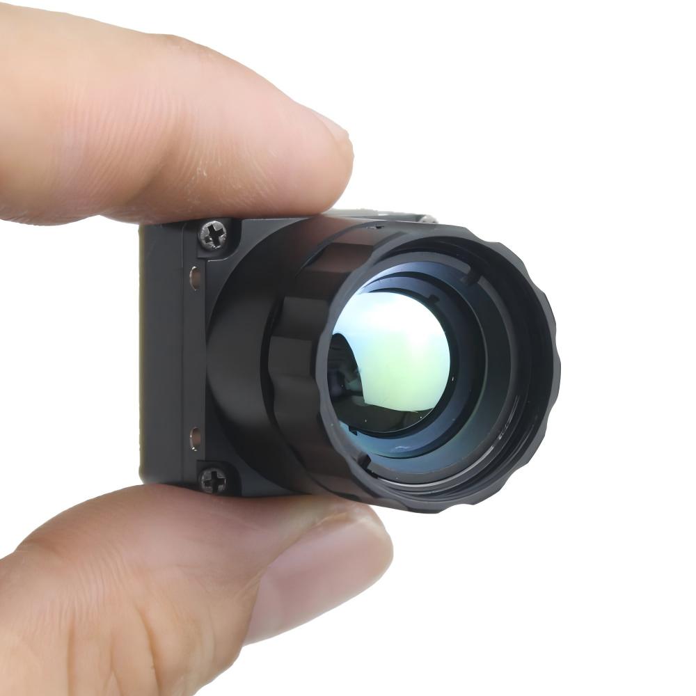
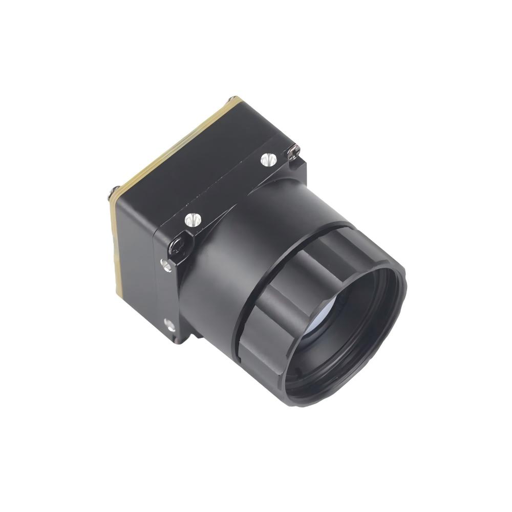
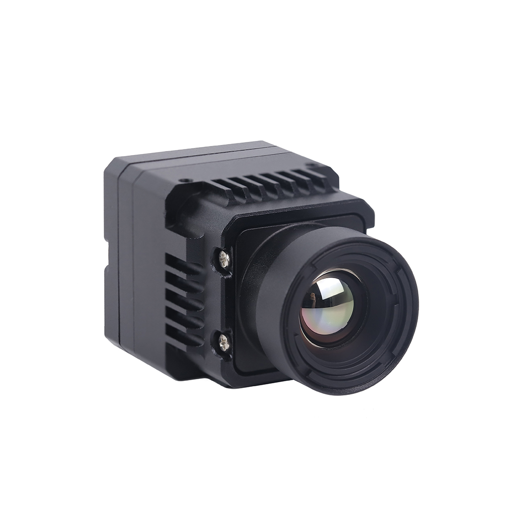
640*512 ASIC Thermal Sensor Module
Uncooled Infrared Mini 640*512 ASIC Thermal Imaging Camera Module For Drones. This module delivers high resolution and rich streaming versatility for professional payloads. |
|
|
Full Specs ➔ |
|
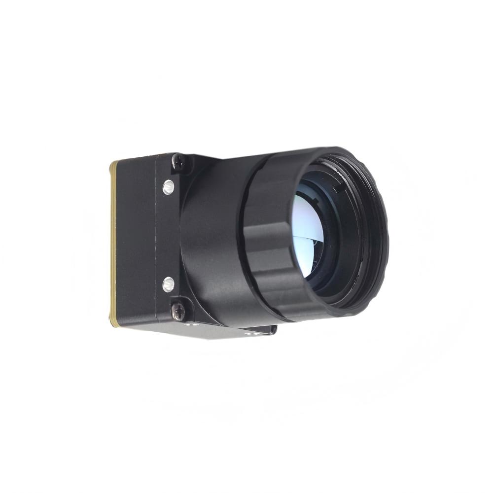
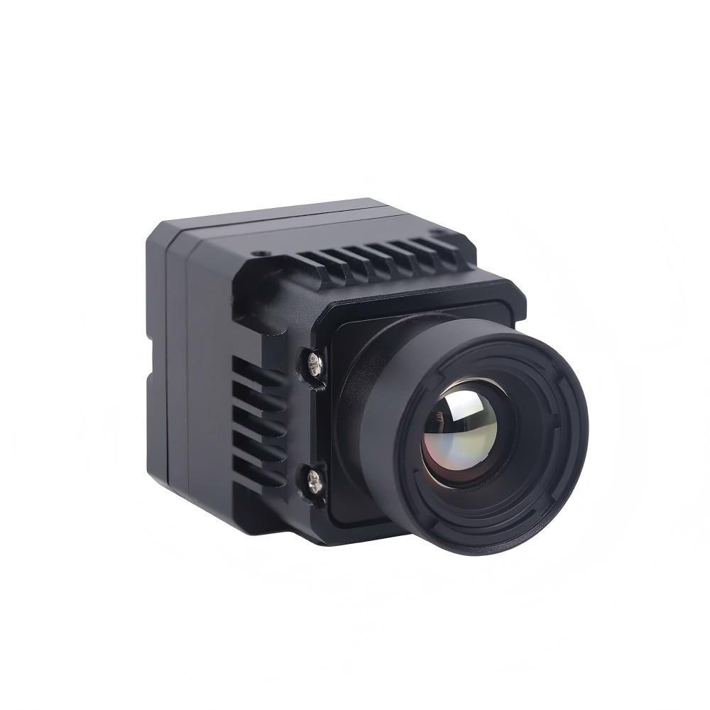
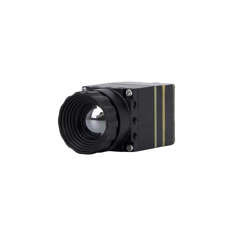
الوحدة الحرارية MD Series بدقة 384x288
Purpleriver industrial-grade thermal imaging module designed for precision and rapid integration. Engineered for compact spaces and versatile connectivity. |
|
|
Full Specs ➔ |
Integration Guidelines for Purpleriver Cores
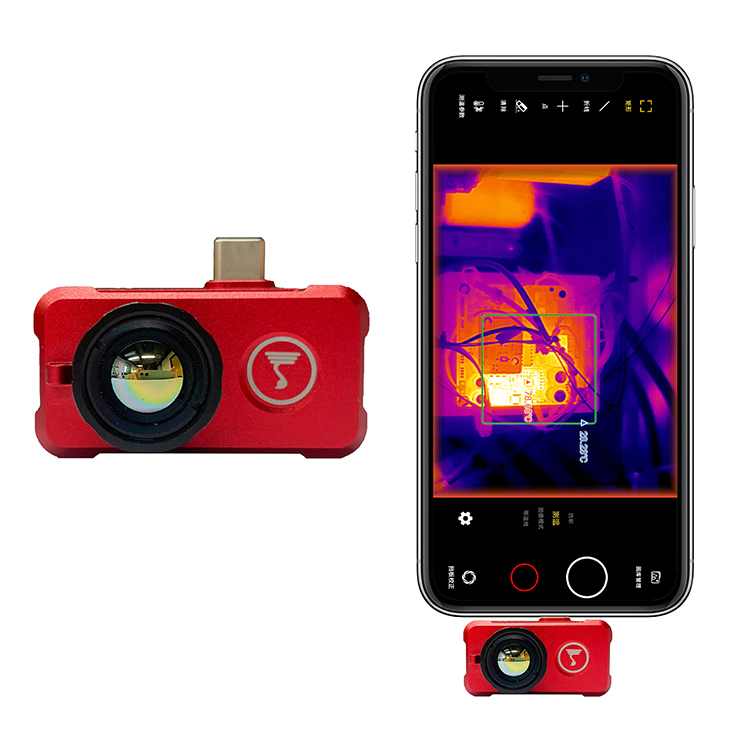
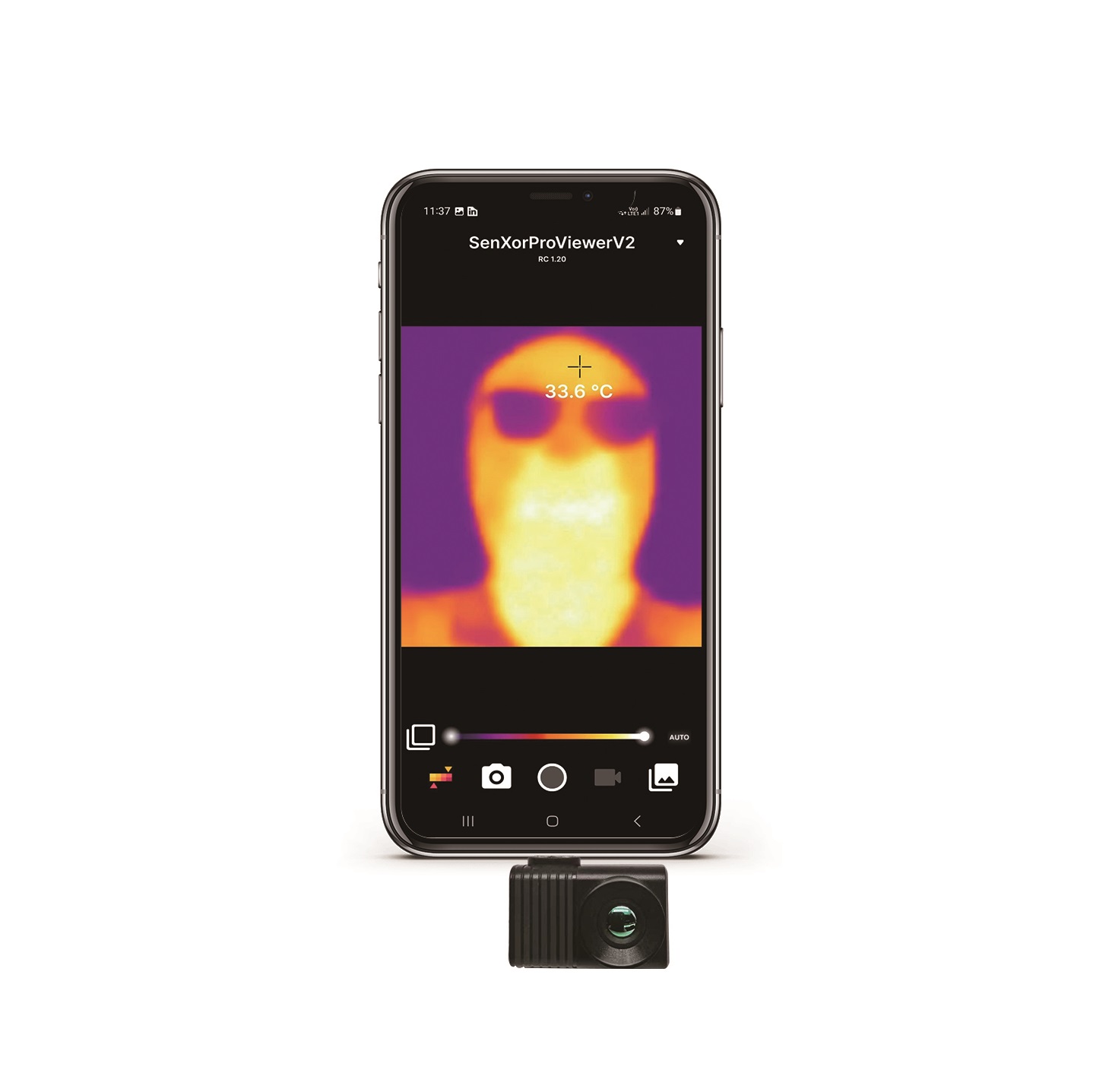
Deploying these versatile uncooled thermal modules enables product development teams to easily scale up production lines. These modules are built on core detector architectures identical to those found in premium uncooled infrared thermal imaging LWIR camera lines. For smaller-scale mobile integration requirements, evaluating how these core thermal architectures compare to ultra-compact, low-power layouts is straightforward. Review our specialized guide on selecting a smartphone thermal imaging camera module guidelines to learn more about balancing SWaP-C (Size, Weight, Power, and Cost) constraints.
الهندسة البصرية واختيار العدسات لكاميرات LWIR
Here is an optical reality check: you cannot run a thermal camera module through standard optical glass. Cheap quartz, silica, or BK7 glass acts like an opaque concrete wall to long-wave infrared energy. If you try it, you will just end up measuring the temperature of the back of your own lens. To pass the 8μm to 14μm spectral band, we have to look to specialized crystalline substrate materials.
When selecting your optical elements, pay close attention to these primary substrates:
- 💎 Germanium (Ge): This is the king of thermal materials. Germanium has an exceptionally high refractive index of roughly 4.0, which means you can design highly efficient, thin lenses with minimal optical aberration. It also has incredibly low dispersion qualities. But Germanium has a nasty Achilles' heel: thermal runaway. If your camera is deployed in a steel mill or in direct desert sun where the lens temp creeps past 60°C, Germanium’s absorption rate spikes exponentially. Eventually, the glass turns black to LWIR energy, and your image completely drops out.
- 🔬 Chalcogenide Glass: This is a synthetic chalcogen-based amorphous mixture (usually incorporating elements like selenium, arsenic, and sulfur). It is a fantastic option for automated, high-volume manufacturing because you can mold the lens under high heat rather than diamond-turning it. While its optical properties are slightly inferior to pure Germanium, it is much cheaper and thermal runaway is far less of an issue, making it a stellar option for industrial security setups.
- 🔍 Silicon (Si): While silicon works best in the Mid-Wave Infrared (MWIR) 3μm to 5μm band, thin-profile silicon element configurations can be designed to work reliably in low-cost, short-range LWIR applications. It is incredibly durable, abundant, and offers a tough, scratch-resistant surface.
Critical Optical Formulas
When calculating the physical limits of your system on the drawing board, keep these two fundamental optical formulas handy:
1. Instantaneous Field of View (iFOV)
$$iFOV = \frac{p}{f}$$
Where:
- 📌 iFOV: The spatial resolution of a single pixel in milliradians (mrad).
- 🎛️ p: The physical pixel pitch of the detector array (e.g., $12\mu\text{m} = 0.012\text{ mm}$).
- 📏 f: The effective focal length of the lens assembly in millimeters (mm).
Calculating the iFOV is critical—it tells you the absolute smallest physical feature size your sensor can resolve at a specific target distance.
2. Sensor Field of View (FOV)
$$FOV = 2 \cdot \arctan\left(\frac{W}{2f}\right)$$
Where:
- 🎚️ W: The total physical dimension of the sensor array width or height in millimeters ($W = N \times p$, where $N$ is the active pixel count along that axis).
- 📏 f: The focal length of the lens in millimeters.
Real-World Design Example
Say you are building a system around a 640x512 core with a 12μm pixel pitch ($0.012\text{ mm}$), and you pair it with a 19mm lens.
- First, find the physical width ($W$) of your sensor: $640 \text{ pixels} \times 0.012\text{ mm} = 7.68\text{ mm}$.
- Now, calculate the spatial resolution ($iFOV$): $\frac{0.012\text{ mm}}{19\text{ mm}} = 0.63\text{ mrad}$. That means at a distance of 100 meters in the field, a single pixel covers a square just 6.3 cm across ($0.63\text{ mrad} \times 100\text{ m}$).
- Next, calculate your horizontal field of view ($FOV$): $2 \cdot \arctan\left(\frac{7.68}{38}\right) = 2 \cdot \arctan(0.202) \approx 2 \cdot 11.43^\circ = 22.86^\circ$.
Lens Coatings
Because materials like Germanium have high refractive indices, reflections are brutal; untreated lenses reflect away almost 36% of incoming heat. To fix this, manufacturers apply deep anti-reflective (AR) coatings. For external-facing elements, engineers spec a rugged, Diamond-Like Carbon (DLC) coating. This ultra-hard barrier protects the expensive Germanium from high-speed sand scour, salty marine spray, and caustic petrochemical fumes on factory floors.
الأسئلة الشائعة المتعمقة الشاملة (مرجع تقني)
Can I interface a high-resolution CMOS/ROIC thermal sensor camera module directly with low-power microcontrollers like Arduino, or is a performance board like Raspberry Pi required?
What are the engineering differences between Vanadium Oxide (VOx) and Amorphous Silicon (a-Si) detectors in uncooled CMOS LWIR thermal modules?
What specific power supply noise isolation methods are required to prevent visual artifacts on a CMOS thermal sensor camera module?
📚 References & Further Reading
- Industry Standard: Learn more about external cable and signal integration from رجل الكابل المحوري الصغير.
- Scientific Baseline: Explore the technological history and physical theories of microbolometer structures at التصوير بالأشعة تحت الحمراء في ويكيبيديا.
- Embedded Linux Platforms: Learn how to connect uncooled digital cores to SBC hardware in our guide on choosing a thermal camera module for Raspberry Pi.
- Mobile Form Factor Calibration: Read our handbook on choosing a smartphone thermal imaging camera module guidelines.
- Optoelectronic Cores: Deepen your understanding of large-format uncooled core assemblies by reading about uncooled infrared thermal imaging LWIR cameras.