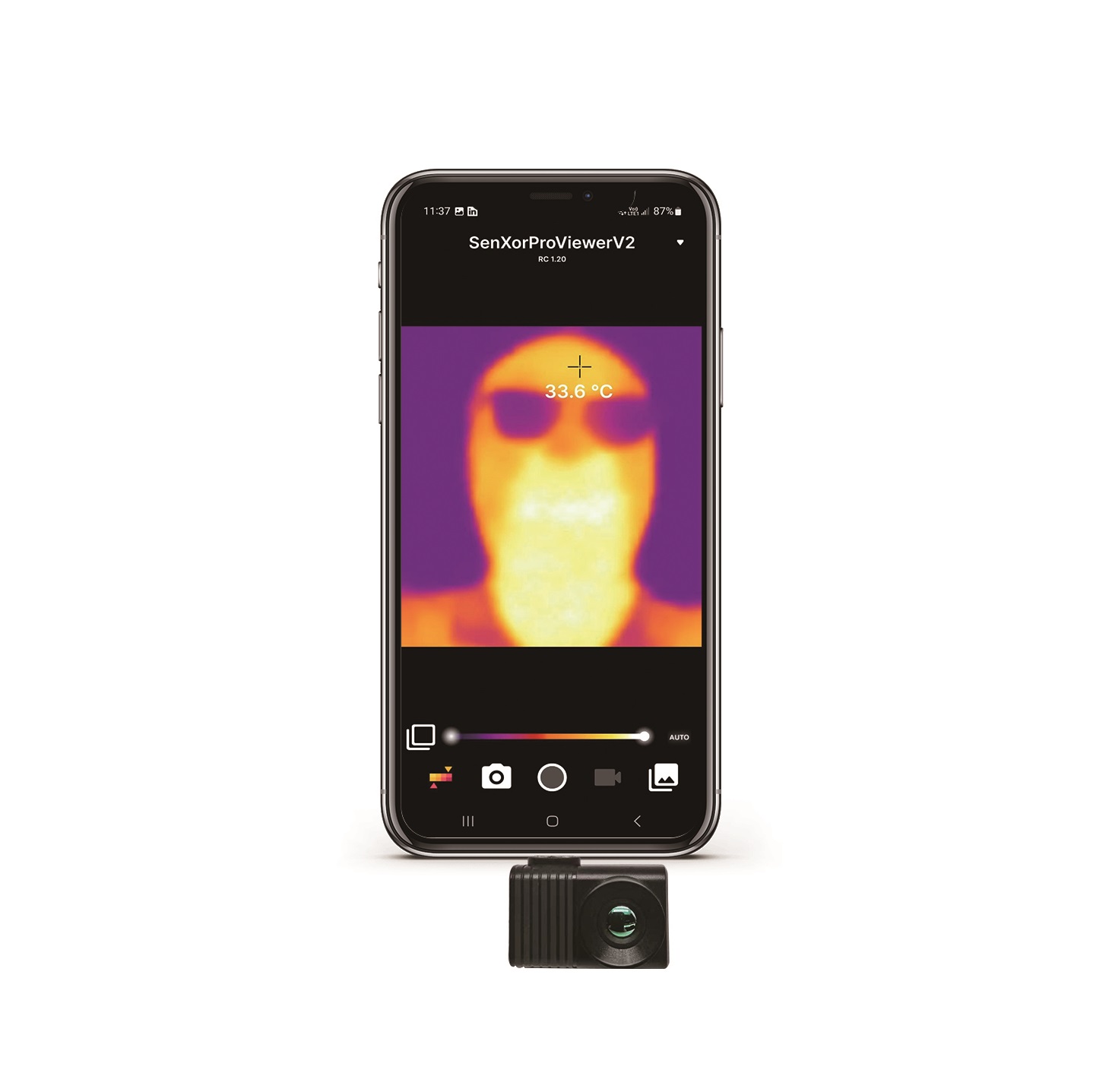


Best CVBS Thermal Camera Module: Low-Latency Analog Cores for Drones & Systems
2026年9月22日
OEM UART Thermal Camera Module: High-Resolution LWIR Cores for Drones & Robotics
2026年9月23日
Analog Thermal Camera Core Guide: Low-Latency CVBS Modules for FPV, DIY Optics & OEM
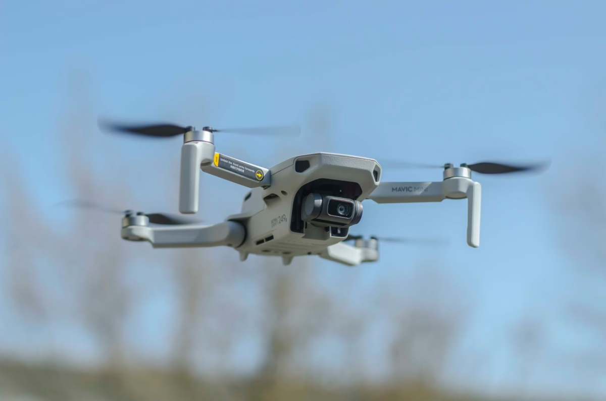
In high-speed unmanned aerial systems (UAS), tactical electro-optical payloads, and handheld hunting optics, latency is the primary barrier to operational performance. Modern digital video pipelines—leveraging MIPI-CSI, USB UVC, or Ethernet IP streams—introduce systemic encoding, packetization, and frame-buffering delays that range from 30 milliseconds to over 150 milliseconds. For a First-Person View (FPV) drone navigating through dense tree canopies at 80 km/h or a targeting goggle tracking rapid kinetic motion, even a 50-millisecond lag causes significant spatial displacement. This critical operational constraint has driven an engineering renaissance for the analog thermal camera core: an electro-optical module that converts uncooled Long-Wave Infrared (LWIR) sensor data directly into an instantaneous Composite Video Baseband Signal (CVBS / PAL / NTSC) with near-zero latency.
Integrating an analog thermal core bypasses complex operating systems, host driver stacks, and software overhead. By combining a 12μm Vanadium Oxide (VOx) microbolometer array with dedicated Application-Specific Integrated Circuit (ASIC) image processing and high-speed Digital-to-Analog Converters (DAC), these cores output standard 75-ohm composite analog video directly into analog 5.8 GHz video transmitters (VTX), legacy monitors, micro-OLED displays, and tactical feeds. This guide delivers a complete engineering blueprint for systems integrators, hardware developers, and DIY optical engineers seeking to maximize dynamic thermal responsiveness, reduce payload weight down to 21mm form factors, and deploy robust thermal sensing systems.
Содержание
- 👉 1. Architectural Overview: Demystifying the Analog Thermal Camera Core
- 👉 2. The LWIR-to-CVBS Signal Processing Pipeline
- 👉 3. Latency Benchmarking: CVBS vs. USB, MIPI, and IP Streams
- 👉 4. OEM Hardware Comparison: Mini 640 vs. MD Series 384
- 👉 5. Electrical & RF Integration for FPV Airframes & Gimbal Payloads
- 👉 6. Designing Custom DIY Optics: Thermal Scopes & Handheld Monoculars
- 👉 7. Hardware Pinouts, 75Ω Transmission Lines, and Command Protocols
- 👉 Углублённый инженерный FAQ
1. Architectural Overview: Demystifying the Analog Thermal Camera Core
A persistent misconception in optoelectronics is that an "analog thermal camera core" uses a legacy analog sensor array. In reality, all contemporary microbolometer detectors are solid-state semiconductor devices fabricated on Read-Out Integrated Circuits (ROICs) that operate natively in the digital domain. An analog thermal camera core refers to an integrated, SWaP-optimized module that marries an advanced uncooled LWIR detector with an onboard image signal processor (ISP) and an ultra-fast video DAC, delivering a plug-and-play CVBS (композитный видеосигнал основной полосы частот) analog feed over a single unbalanced conductor pair.
At the physical core of these systems lies a focal plane array (FPA) composed of thermally isolated micro-resistors manufactured typically from Vanadium Oxide (VOx). When thermal infrared radiation within the 8μm to 14μm atmospheric transmission window strikes these microscopic suspended membranes, their electrical resistance changes proportionately to the incident target temperature via their Temperature Coefficient of Resistance (TCR). The underlying CMOS ROIC digitizes these subtle resistance deltas using multi-channel, high-resolution integrated analog-to-digital converters, typically operating with a 14-bit or 16-bit depth.
The fundamental challenge in tactical thermal imaging is converting this high-dynamic-range raw digital stream into visually interpretable, actionable spatial imagery without introducing pipeline lag. In modern digital architectures, the processed thermal data must be encapsulated into USB packets, encoded via lossy H.264/H.265 compression algorithms, or routed through high-speed differential pairs (MIPI-CSI) to an intermediate host processor. That host processor must initialize hardware frame buffers, schedule operating system tasks, and manage display compositor stacks, which inevitably introduces processing jitter and buffering latency exceeding tens to hundreds of milliseconds.
Conversely, an analog thermal camera core offloads all spatial processing, dynamic range compression, non-uniformity correction (NUC), and color palette mapping directly to a dedicated hardware pipeline executed inside an onboard Field-Programmable Gate Array (FPGA) or custom Application-Specific Integrated Circuit (ASIC). Once calibrated and mapped, the digital raster is passed directly to a high-speed video reconstruction DAC that synthesizes a standardized analog composite waveform (1.0V peak-to-peak into 75Ω). The output adheres strictly to ITU-R BT.470 or SMPTE 170M standards for PAL (625 lines, 50 fields/second) or NTSC (525 lines, 60 fields/second).
The result is a self-contained electro-optical engine that requires nothing more than direct DC power (typically 3.3V to 5V) to begin outputting zero-overhead thermal imagery straight to analog RF modulators, cockpit multi-function displays (MFDs), micro-displays, or tactical feeds without an external single-board computer (SBC) or operating system kernel.
This streamlined architecture delivers immediate operational advantages across rugged deployments:
- ✅ Deterministic Frame Delivery: Video lines are converted and transmitted scanline-by-scanline without frame-queuing jitters or operating system thread preemption.
- ✅ Instant-On Initialization: Video appears within 2 to 4 seconds of cold boot, completely eliminating Linux/Android boot delays in urgent tactical scenarios.
- ✅ Immunity to Software Freezes: Without dynamic link libraries, OS kernels, or USB enumeration handshakes, the feed cannot lock up from buffer overflows or driver crashes.
- ✅ Extreme SWaP Efficiency: Eliminates the bulk, heat dissipation requirements, and electrical load of host processing boards like Raspberry Pi or Jetson platforms.
2. The LWIR-to-CVBS Signal Processing Pipeline
The internal operational pipeline of an industrial-grade analog thermal core balances microbolometer physics, high-speed computational imaging algorithms, and precision mixed-signal electronics. Understanding this data flow allows system designers to optimize lens choices, digital zoom limits, and dynamic range scaling.
⚙️ Stage 1: Raw Calibration: 2-Point NUC and Defective Pixel Correction
Each individual pixel in a 640×512 or 384×288 microbolometer array possesses distinct thermal coefficients, semiconductor manufacturing variances, and bias drift. The initial stage of the ASIC pipeline applies коррекции неоднородности (NUC). Using coefficients derived during factory optical calibration and fine-tuned by periodic internal shutter (or shutterless algorithmic calibration), the raw reading is normalized across every single pixel:
Scorr = Гij · Sнеобработанный + Oij
Где Gij represents the pixel-specific gain matrix and Oij represents the dynamic offset map. Concurrently, Bad Pixel Replacement (BPR) algorithms identify defective or blind bolometer elements, substituting their values with dynamic median interpolations of adjacent healthy pixels to eliminate fixed-pattern visual artifacts.
⚙️ Stage 2: High-Dynamic-Range Compression and DDE
Raw thermal scenes typically exhibit dynamic ranges exceeding 14 bits (16,384 discrete levels of thermal intensity), whereas standard human displays and analog video standards only support 8 bits per channel (256 grayscale levels). An analog core applies proprietary dynamic range compression algorithms, such as цифровое улучшение деталей (DDE) or advanced histogram equalization. This separates high-amplitude, low-frequency scene elements (such as broad terrain or uniform sky backgrounds) from subtle, low-amplitude, high-frequency details (such as a human target hidden in foliage or a drone motor rotor hub).
⚙️ Stage 3: LUT Application and Video Timing Synthesis
Once compressed to 8-bit space, the pixel data is mapped through programmable Look-Up Tables (LUTs) to output preferred viewing palettes: White Hot, Black Hot, Ironbow, Rainbow, or high-contrast tactical palettes. The pixel matrix is then fed into an onboard video display controller that reformats the digital image grid into interlaced video fields, appending precise horizontal blanking intervals, color bursts (for colorized CVBS feeds), and vertical synchronization pulses.
⚙️ Stage 4: Digital-to-Analog Conversion and Reconstruction Filtering
Finally, the reconstructed digital stream drives an onboard high-speed 10-bit video DAC. The raw, stepped analog voltage exiting the DAC passes through an active low-pass reconstruction filter (typically an active 6th-order Butterworth or Bessel filter design) to suppress out-of-band quantization noise and high-frequency clock harmonics. The final signal emerges as a clean, standardized 1.0 Vp-p signal ready to drive a standard 75 Ω coaxial termination directly into analog transmission gear.
3. Latency Benchmarking: CVBS vs. USB, MIPI, and IP Streams
In high-speed situational awareness, tactical navigation, and dynamic gimbal stabilization, overall system response time is limited by sensor-to-display latency. Digital interfaces introduce a compounding series of temporal buffers that significantly lag behind pure analog transmission.
| Типичная задержка | Pipeline Latency (Glass-to-Glass) | Jitter / Frame Variability | Processing Bottlenecks & Hardware Dependency |
|---|---|---|---|
| Native CVBS (Analog) | < 8 ms (Near Zero) | ± 0.1 ms (Deterministic) | Sensor DAC to RF Transmitter; zero operating system overhead; line-by-line broadcast. |
| MIPI-CSI-2 | 15 – 35 ms | ± 2.0 ms | Requires embedded Linux/RTOS host SoC (e.g., Jetson, RK3588); driver buffer pools and frame grabber queues. |
| USB 2.0 / 3.0 (UVC) | 45 – 90 ms | ± 15.0 ms | Host USB stack, UVC driver abstraction, OS thread scheduling, user-space rendering engines. |
| Ethernet (RTSP / IP) | 100 – 250+ ms | ± 30.0 ms | H.264/H.265 compression GOP buffers, network encapsulation, transmission packet queues, client-side de-jitter decoding buffers. |
The Real-World Engineering Impact of Latency
To put these figures into physical perspective: an FPV drone operating at a standard search-and-rescue or kinetic sprint velocity of 20 m/s (72 km/h) travels 0.14 meters (14 cm) during a 7 ms analog CVBS transmission cycle. If the same platform relies on a USB UVC stream with an average 60 ms glass-to-glass latency, the drone covers 1.2 meters before the remote pilot or flight controller receives visual verification of an obstacle.
Under an RTSP IP video pipeline operating at a conservative 150 ms delay, the vehicle traverses 3 full meters before an obstacle is displayed. For precision piloting, manual close-quarters flight, and low-altitude terrain navigation, analog CVBS remains the most deterministic, reliable protocol for human-in-the-loop control.
For bench-top development and initial hardware prototyping of micro-optics without custom carrier boards, engineers frequently leverage peripheral development components—such as carrier modules and breakout hardware available within the Waveshare ecosystem—to verify pinout connections and test baseline video performance before transitioning to dedicated printed circuit boards.
4. OEM Hardware Comparison: Mini 640 vs. MD Series 384
Selecting an analog thermal camera core requires matching resolution, pixel pitch, optical magnification, and physical integration constraints to the target application. Below is a detailed technical comparison of two industry-standard modules specifically engineered for low-latency CVBS, multi-interface flexibility, and SWaP-C (Size, Weight, Power, and Cost) optimization.
| Метрика спецификации | Неохлаждаемый LWIR-модуль тепловизора Mini 640 | Тепловизионный модуль камеры MD Series 384x288 |
|---|---|---|
| Технология детектора | Неохлаждаемый VOx микроболометр | Неохлаждаемый VOx микроболометр |
| Разрешение матрицы | 640 × 512 (640 × 480 optional) | 384 × 288 |
| Шаг пикселя | 12 мкм | 12 мкм |
| Спектральный отклик | 8 мкм – 14 мкм (LWIR) | 8 мкм – 14 мкм (LWIR) |
| Тепловая чувствительность (NETD) | ≤ 40 mK @ f/1.0, 300K | ≤ 40 mK @ f/1.0, 300K |
| Native Analog Video Output | CVBS (PAL 50Hz / NTSC 60Hz selectable) | CVBS (PAL / NTSC configurable) |
| Цифровые видеоинтерфейсы | High-speed USB / Digital Stream | Multi-Bus: Concurrent MIPI / USB / CVBS |
| Standard Lens Offerings | 5 / 9 / 13 / 18 / 35 / 50 / 75 / 100 / 150 мм | Standard fixed focal optics (custom mounts available) |
| Form Factor Dimensions | 21 мм × 21 мм (Ultra-compact core) | Compact industrial footprint |
| Engineering Origin | UAV-optimized SWaP-C thermal package | Ex-Huawei HiSilicon & HKUST optical engineering team |
| Адаптация к окружающей среде | High stability, wide temperature envelope | Industrial-grade precision, temperature monitoring |
Deep Architectural Dive: Mini 640 Series
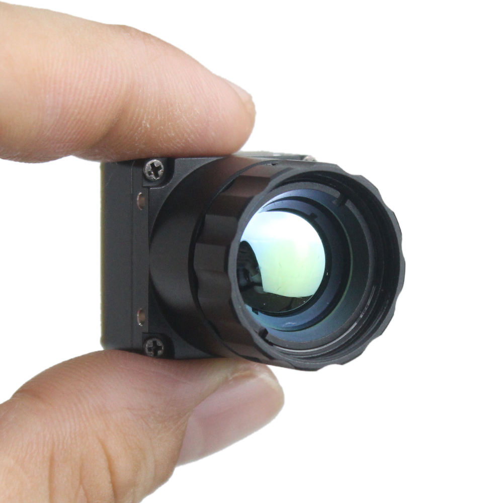
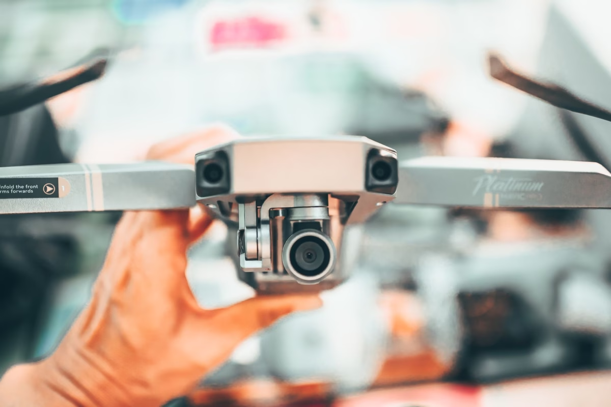
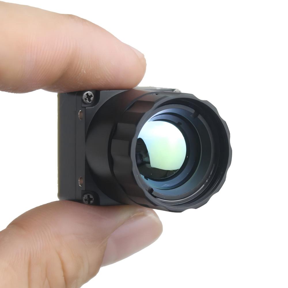
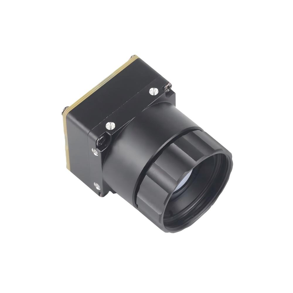
The → Неохлаждаемый LWIR USB мини-модуль ядра тепловизионной камеры 640*512 для дронов, аналогичный DJI represents a major achievement in SWaP-optimized thermal engineering. Measuring just 21 мм × 21 мм, this module delivers high thermal resolution without penalizing payload weight budgets. Built specifically for integration into micro-gimbals and compact aerial airframes (such as tactical quadcopters and fixed-wing reconnaissance platforms similar to DJI Enterprise or custom systems), it provides crisp spatial detail through its 640×512 detector matrix (with 640×480 resolution optional).
The module stands out for its extensive compatibility with factory-calibrated continuous and fixed Germanium optics, offering focal lengths of 5 мм, 9 мм, 13 мм, 18 мм, 35 мм, 50 мм, 75 мм, 100 мм и 150 мм. This broad range allows engineers to configure payloads for wide-angle navigation (e.g., 5mm or 9mm for tight situational flying) or long-range tactical standoff identification (e.g., 75mm to 150mm for border surveillance and search-and-rescue). When operating in its native CVBS mode, the internal processing engine handles downsampling and scanline mapping automatically, outputting clean, tear-free analog frames directly to onboard 5.8 GHz analog VTX units or micro-monitors.
Посмотреть детали продукта и цены ➔
Deep Architectural Dive: MD Series 384
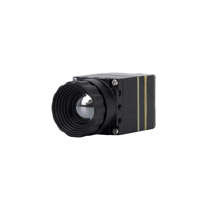
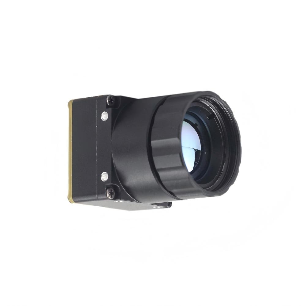
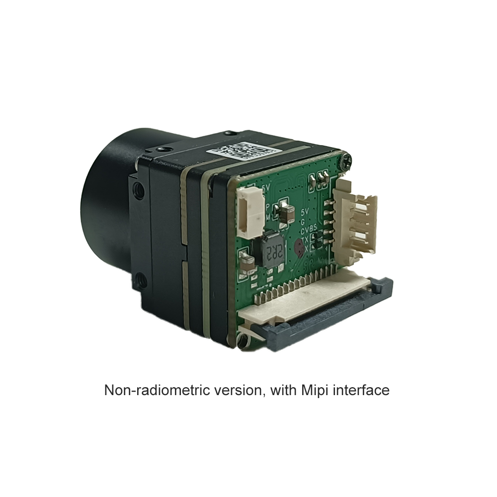
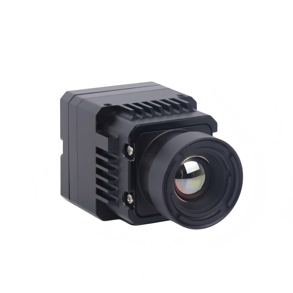
The → Серия MD 384x288 неохлаждаемый инфракрасный тепловизионный модуль камеры (Purpleriver thermal camera module) is engineered specifically for industrial-grade precision in applications such as security, continuous temperature monitoring, and drone integration. Developed by an engineering team with backgrounds from the Hong Kong University of Science and Technology (HKUST) and former Huawei HiSilicon semiconductor architects, this core features a unique concurrent output architecture: MIPI, USB, and CVBS.
This multi-interface topology allows system designers to route an uncompressed digital MIPI stream to an onboard AI edge-compute module (such as an NVIDIA Jetson Orin or Rockchip NPU for real-time target bounding-box detection), while simultaneously routing the native CVBS signal to an analog RF transmitter for zero-latency manual flight control. Featuring a refined 12μm pixel pitch, the MD Series delivers high thermal sensitivity and sharp thermal imaging in a compact, plug-and-play profile. Backed by extensive OEM/ODM customization capabilities, this module can be tailored to meet specialized optical mounts, custom pinouts, and strict mechanical envelope constraints.
Посмотреть детали продукта и цены ➔
5. Electrical & RF Integration for FPV Airframes & Gimbal Payloads
Integrating an analog thermal camera core into an FPV drone or stabilized robotic gimbal requires careful attention to electrical noise, power conditioning, and RF interference. Switching regulators, high-current brushless electronic speed controllers (ESCs), and high-power video transmitters can introduce severe artifacts into the analog thermal video signal if not properly isolated.
⚙️ 1. Power Supply Decoupling and Filtering
Uncooled microbolometers are exceptionally sensitive to power rail fluctuations; high-frequency voltage ripple directly modulates the ROIC bias voltages, manifesting as horizontal scrolling lines, periodic rolling bars, or elevated fixed-pattern noise across the analog display.
To ensure clean operation in electrically noisy environments, never power an analog thermal core directly from the main flight battery (VBAT). Brushless motors generate severe inductive voltage spikes (back-EMF) that frequently exceed 40V on 6S LiPo setups during active motor braking. Instead, feed the thermal core using a dedicated low-noise linear low-dropout regulator (LDO) or an efficient switching step-down converter followed by an LC filter. A 100μH inductor coupled with a low-ESR 470μF electrolytic capacitor in parallel with a 0.1μF ceramic capacitor will successfully isolate dynamic throttle transients. Furthermore, ensure the regulator provides a stable 5.0V DC rail with at least 1.5A continuous current capacity to absorb initial shutter-solenoid actuation current peaks.
⚙️ 2. Grounding Topologies and Ground Loop Elimination
Composite video (CVBS) uses an unbalanced, single-ended transmission standard where visual data is referenced directly to system ground. Any minute voltage differential between the camera ground and the VTX ground will directly corrupt the video signal.
Integrators must establish a star ground topology: route the analog thermal camera core's ground pin directly to the same ground plane terminal used by the 5.8 GHz VTX. This eliminates ground loop hum bars (dark horizontal bands drifting vertically across the monitor). For video wiring, route the signal using miniature 75-ohm micro-coaxial cable (such as RG-178 or 1.13mm micro-coax) rather than simple unshielded silicone wire. Solder the braided shield directly to video ground at both ends to protect the high-impedance video signal from RF radiation emitted by high-power transmitters (e.g., 1W–2.5W VTX units) and digital telemetry links.
⚙️ 3. Real-World Applications: Automotive Obstacle Detection
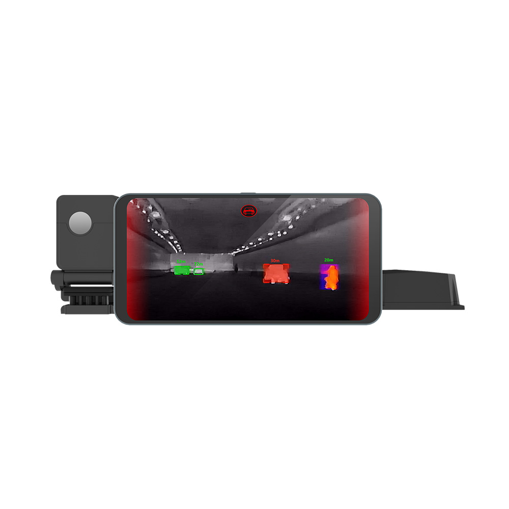
The exact electrical decoupling and high-vibration isolation principles that safeguard dynamic FPV drones apply directly to automotive night vision retrofits. For detailed real-world implementations using LWIR camera modules to cut through headlight glare, thick dust, and heavy fog in vehicular platforms, explore this guide to очень интересная и практичная автомобильная камера тепловизионного изображения.
6. Designing Custom DIY Optics: Thermal Scopes & Handheld Monoculars
The ultra-compact profile of modern analog cores (especially the 21mm square cross-section of the Mini 640) has simplified the development of custom DIY thermal monoculars, 3D-printed handheld spotting devices, and clip-on tactical scopes. Building a complete optical instrument around an analog thermal module eliminates the complexity and power drain of external microprocessors.
Optical Stack Architecture
When engineering a custom optic, the hardware stack breaks down into four essential electro-optical stages:
- ⚙️ Germanium Objective Lens: Standard optical glass completely blocks the Long-Wave Infrared spectrum (8–14μm). A specialized optical lens made of metallic Germanium or specialized chalcogenide glass with an anti-reflective (AR) hard-carbon diamond coating is mandatory. A short focal length (e.g., 9mm to 13mm) yields an expansive Field of View (FOV) suitable for short-range scanning and navigation. A long focal length (e.g., 35mm, 50mm, or 75mm) concentrates the optical resolution on distant targets, functioning as a high-magnification thermal rifle optic or wildlife survey tracker.
- ⚙️ Display Engine Pairing: The primary objective in DIY analog optic design is pairing the core directly with a micro-display module (such as a 0.39-inch or 0.71-inch Sony Micro-OLED or FLCOS panel) that accepts native composite video inputs. By feeding the CVBS output directly into the display's driver board, the system operates without an intermediate microcontroller, eliminating software latency and boot-time delays.
- ⚙️ Eyepiece / Diopter Assembly: High-performance ocular lenses with mechanical diopter adjustment (-4 to +2 dpt) allow users to adjust focus onto the virtual display surface without optical distortion.
- ⚙️ Power Management: A single high-capacity 18650 or 21700 lithium-ion cell paired with a high-efficiency synchronous buck-boost converter provides 4 to 8 hours of continuous, silent operation.
For systems integrators working across international supply chains or sourcing specialized optomechanical hardware components, enterprise platforms like КУЯНГ offer broad selections of electro-optical structural assemblies and tactical accessories.
For international engineering teams seeking technical reference materials across regional design centers, consult our comprehensive Russian guide to tiny thermal modules or review the Arabic MIPI thermal module architecture breakdown.
7. Hardware Pinouts, 75Ω Transmission Lines, and Command Protocols
Implementing an OEM analog core into a custom enclosure or avionics stack requires configuring physical layer terminations and digital serial commands for dynamic operational control.
Standard Interface Pinout Configuration
Most industrial micro-cores utilize a multi-pin Hirose or JST ultra-fine-pitch connector to expose both power, analog signaling, and serial control lines:
- ⚙️ Pin 1: VCC (3.6V to 5.5V DC regulated input)
- ⚙️ Pin 2: GND (Primary power ground return)
- ⚙️ Pin 3: CVBS_OUT (Standard composite analog video, 1.0 Vp-p into 75Ω)
- ⚙️ Pin 4: AGND (Dedicated analog video ground shield)
- ⚙️ Pin 5: UART_RX (3.3V TTL command input for register control)
- ⚙️ Pin 6: UART_TX (3.3V TTL telemetry and command acknowledgment)
Video Standard Matching & 75-Ohm Terminations
To maintain signal fidelity and prevent visual reflections or blurring, the CVBS output trace must be routed as a controlled-impedance line:
- ⚙️ The 75-Ohm Rule: The video DAC has an output impedance calibrated to match a standard 75 Ω load. The display receiver or VTX must terminate the line with an internal 75 Ω shunt resistor to ground. If terminated with a high-impedance (e.g., 10 kΩ) load, the signal amplitude doubles to 2.0 Vp-p, washing out scenes into blown-out white levels. Conversely, double-termination (parallel 75 Ω loads resulting in 37.5 Ω) drops the signal amplitude to 0.5 Vp-p, resulting in dark, noisy video.
- ⚙️ PAL vs. NTSC Timing: The core can be configured through hardware strapping pins or software registers to output either PAL (720×576 effective lines @ 50 fields/second) or NTSC (720×480 effective lines @ 60 fields/second). System integrators should configure the core to match the native display refresh rate of their micro-OLED panel or RF receiver.
Serial Control Protocols (UART TTL)
While the video signal flows through the analog line, internal camera states (e.g., triggering a manual NUC calibration, switching between White-Hot and Ironbow palettes, zooming 2×/4×/8×, or overlaying crosshairs) are governed by sending hexadecimal packets across a standard 3.3V TTL UART bus (typically configured at 115200 or 9600 baud, 8 data bits, no parity, 1 stop bit).
A standard Pelco-D format or proprietary command packet structure uses the following framing:
[Header: 0xAA] [Command ID] [Param 1] [Param 2] [Checksum] [Tail: 0x55]
- ⚙️ Trigger Shutter (NUC):
0xAA 0x01 0x00 0x00 0x01 0x55(Engages the internal mechanical shutter flag to refresh the sensor offset map). - ⚙️ Toggle Palette:
0xAA 0x02 0x01 0x00 0x03 0x55(Cycles between White-Hot, Black-Hot, and color LUTs). - ⚙️ Digital Zoom:
0xAA 0x03 0x02 0x00 0x05 0x55(Executes instantaneous 2× center-crop pixel interpolation).
This physical separation of command logic (digital serial UART) and low-latency video streaming (CVBS) provides an ideal operational topology for embedded microcontrollers, drone flight controllers, and mechanical toggle switches.
Углублённый инженерный FAQ
Can an analog thermal camera core connect directly to an analog FPV video transmitter (VTX) or composite screen?
Is there truly an 'all-analog' thermal sensor, or how does an analog thermal core work?
Can I use your 640x512 or 384x288 module to replace or upgrade an existing thermal scope or DIY monocular core?
Conclusion & Integration Support
The modern analog thermal camera core bridges high-resolution uncooled infrared sensor technology with ultra-low-latency video transmission. Whether you are integrating a sub-miniature Мини 640 core into a tactical search-and-rescue FPV drone frame, retrofitting an uncooled sensor into a stabilized marine gimbal, or manufacturing a custom handheld thermal monocular, native CVBS output provides immediate responsiveness, simplified wiring, and high SWaP-C performance.
For custom optical engineering support, specialized pinout variations, OEM/ODM production requirements, or lens customization, contact our hardware engineering division through our product portals:
- 👉 Explore the Mini 640 LWIR Thermal Core Module
- 👉 Evaluate the MD Series 384 Multimodal Thermal Engine
📚 Ссылки и дополнительная литература
- Отраслевой стандарт: Sourcing and optomechanical hardware integration via КУЯНГ
- Development Ecosystem: Prototyping carrier boards and modular hardware platforms at Waveshare
- Связанное руководство: In-depth automotive obstacle avoidance design in our guide to очень интересная и практичная автомобильная камера тепловизионного изображения
- Technical Blueprint (Arabic): Embedded sensor integration manual at دليل وحدة الكاميرا الحرارية MIPI عالية الدقة
- Technical Blueprint (Russian): Miniature sensor design architecture in our руководстве по крошечным тепловизионным модулям