
Radiometric Thermal Camera Modules: The Ultimate Guide for OEM Industrial Integration
2026年8月21日
True IR vs. Near-Infrared: Ultimate Guide to True Thermal Sensor Modules
2026年8月24日

CMOS Sensor Selection & Integration: Commercial Sourcing Guide for AI & Thermal Vision Systems
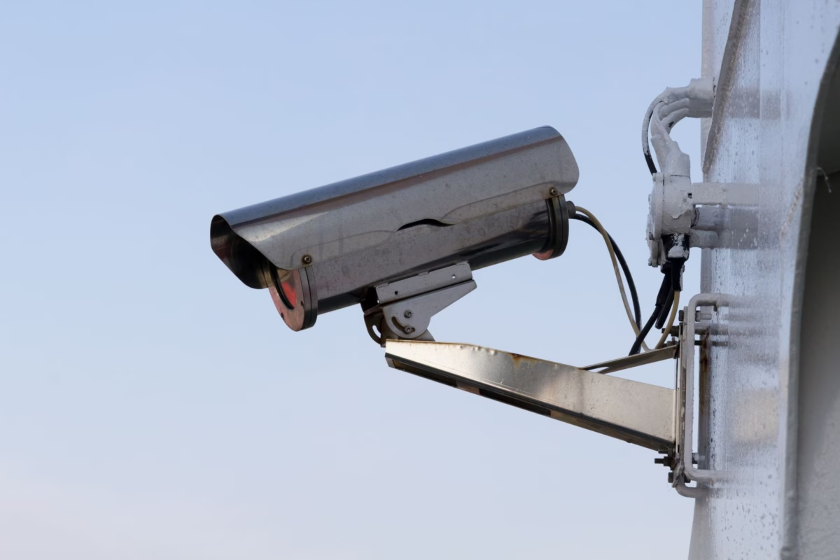
If you've spent any time building automated vision pipelines for aerospace gimbals, factory floor robotics, or perimeter surveillance rigs, you know the score: your computational models are only as good as the raw photons hitting your silicon. Selecting the right CMOS sensor (Complementary Metal-Oxide-Semiconductor) isn't just checking off a spec sheet. It's a foundational hardware decision that dictates your optical quantum efficiency, dynamic range, read noise floor, and thermal dissipation limits when deployed in punishing field conditions. As electro-optical payloads face aggressive size, weight, and power (SWaP) constraints, systems architects have to bridge the gap between visible-spectrum CMOS image sensors and uncooled long-wave infrared (LWIR) detectors to ensure true 24/7 scene awareness.
Here's the deal: cutting-edge edge AI inference falls flat on its face if your image pipeline feeds it clipped dynamic ranges, rolling-shutter spatial artifacts, or unsynchronized multi-spectral frames. You need an airtight balance of optical sensor physics, board-level routing discipline, and practical procurement savvy.
This technical and commercial sourcing guide provides a practical engineering roadmap covering visible CMOS sensor architectures, high-speed optical interfaces, multi-spectral thermal fusion methods, and real-world board-level integration practices. Whether you are assembling an autonomous drone payload, an industrial thermography monitoring rig, or an edge-AI automated defect classification line, this blueprint gives you the electro-optical, interface, and hardware benchmarks required to build and scale rugged, high-reliability vision systems.

Table of Contents
- 👉 1. CMOS Sensor Architecture in Modern Edge Vision
- 👉 2. Multi-Spectral Fusion: Marrying Visible CMOS Sensors with LWIR Thermal Cores
- 👉 3. Industrial Selection Matrix: Noise, Shutter Types, and Interfaces
- 👉 4. Commercial Hardware Comparison: High-Performance Vision & Thermal Modules
- 👉 5. Signal Processing, ASIC Deployment, and Latency Optimization
- 👉 6. Frequently Asked Questions (FAQ)
1. CMOS Sensor Architecture in Modern Edge Vision
The operational landscape for a modern CMOS sensor in edge vision has undergone a massive overhaul over the last decade. Early CMOS devices struggled with brutal dark noise, narrow full-well capacity, and poor quantum efficiency compared to legacy Charge-Coupled Devices (CCD). Today, advanced semiconductor fabrication techniques have pushed CMOS far ahead, making it the bedrock of machine vision, autonomous vehicles, and military optronics.
Pixel Architectures: Front-Side Illumination (FSI) vs. Back-Side Illumination (BSI)
The physical routing of traces, transistors, and photodiodes within the silicon matrix dictates your optical fill factor—the exact ratio of light-sensitive photodiode area to the overall pixel footprint. Migrating across pixel architectures has been one of the biggest leaps in optical engineering:
- ⚙️ Front-Side Illumination (FSI): In legacy FSI layouts, the metal interconnects, power bus lines, and reset gates sit directly on top of the silicon substrate, right between the on-chip microlens and the photodiode. Because incoming photons have to run this metallic gauntlet, a big chunk of light gets scattered, reflected, or absorbed before reaching the active silicon. At steep angles of incidence—typical with wide-angle or low f-number lenses—FSI produces substantial optical crosstalk and severe vignetting, killing Quantum Efficiency (QE) in low-lux settings.
- ✅ Back-Side Illumination (BSI): BSI flips the entire chip layout upside down. The silicon wafer containing the active photodiodes is back-thinned via chemical-mechanical polishing to just a few micrometers. The sensor is oriented so light strikes the rear of the silicon layer directly, completely bypassing the metal routing layer. This direct optical path boosts fill factor close to 100%, driving peak quantum efficiency above 80% to 90% across the visible (400–700 nm) and near-infrared (NIR, 700–1000 nm) spectra.
- ⚙️ 3D Stacked CMOS Architecture: The gold standard for high-throughput edge AI relies on 3D stacked pixel dies. Using Direct Bond Interconnects (DBI) with wafer-to-wafer copper bonding, the pixel photodiode array sits directly on top of a separate, specialized digital substrate. This lower logic layer houses column-parallel Analog-to-Digital Converters (ADCs), dedicated line memory, and custom hardware accelerators. Stacking gives you blazing-fast parallel readouts without eating into light-gathering silicon real estate, knocking sensor readout latency down to the floor.
Dynamic Range Optimization and Low-Noise Readout Circuitry
In the shop, we rarely see pristine, evenly lit test targets. Vision setups mounted on robotic assembly arms, autonomous mobile robots (AMRs), or critical infrastructure towers have to handle bright outdoor sunlight, blinding specular glints off polished metal, and deep shadow detail in the exact same frame. You need a usable dynamic range pushing 100 dB to 120 dB.
To pull this off without clipping highlights or burying shadow detail in noise, modern industrial sensors utilize Dual Conversion Gain (DCG) readouts. In a DCG circuit, each individual pixel contains switchable capacitive loads on its floating diffusion node:
- ⚙️ High Conversion Gain (HCG): Runs with a tiny floating diffusion capacitance, converting small quantities of photo-generated charge into large voltage swings. This drops input-referred read noise down below 1.0 electron RMS, making it exceptional for pulling crisp data out of pitch-black scenes.
- ⚙️ Low Conversion Gain (LCG): Brings a secondary capacitor online to boost well capacity, letting the pixel absorb massive electron counts under intense illumination without saturating the ADC.
When DCG readouts feed into multi-exposure line-interleaved High Dynamic Range (HDR) engines directly inside the onboard Image Signal Processor (ISP), you get clean, artifact-free output frames with balanced tonal curves, completely eliminating the ghosting and motion blur typical of old-school multi-frame temporal blending.
2. Multi-Spectral Fusion: Marrying Visible CMOS Sensors with LWIR Thermal Cores
Visible-light CMOS sensors deliver incredible spatial resolution, rich color data, and crisp edge fidelity when the lighting is right. But because they rely on reflected ambient photons, they hit a wall in pitch-black nights, thick industrial smoke, heavy airborne dust, or pea-soup fog. To deliver dependable 24/7 target tracking, robust hardware setups pair visible CMOS arrays directly with long-wave infrared (LWIR) detectors.
Thermal infrared imaging operates across the 8 µm to 14 µm spectrum, picking up direct blackbody radiation emitted by targets based on their absolute temperature and surface emissivity. Commercial thermal vision relies on uncooled microbolometer focal plane arrays (FPAs)—a solid-state technology covered in depth on the Wikipedia Microbolometer overview—where Vanadium Oxide (VOx) or Amorphous Silicon (a-Si) pixel elements absorb thermal radiation and shift their electrical resistance accordingly.
Physical Parallax and Optical Axis Homography
Look, combining two completely different optical assemblies—a refractive glass lens over a visible CMOS chip alongside a germanium or chalcogenide lens over an LWIR microbolometer—brings immediate mechanical and optical headaches:
- ⚙️ Parallax Disparity: Because the two optical centers are separated by a physical baseline on your payload bracket, the spatial shift between images changes with target distance. At infinity, the parallax shift is negligible; at close inspection ranges (1 to 5 meters), it creates major alignment errors. Precision multi-spectral rigs use real-time affine homography matrices derived from stereoscopic calibration routines to stretch, rotate, and align the visible coordinate space onto the thermal map.
- ⚙️ Focal Length and Field of View (FOV) Matching: Visible CMOS sensors typically feature compact optical formats (such as 1/2.8" or 1/1.8") with tight pixel pitches (1.4 µm to 2.9 µm), yielding 1080p or 4K resolution. In contrast, uncooled thermal sensors utilize wider pixel pitches (12 µm or 17 µm) with standard industrial array formats of 640×512 or 1280×1024. System engineers must meticulously calculate the horizontal and vertical focal lengths to achieve closely matched fields of view across both channels.
Pixel-Level Multi-Spectral Fusion Algorithms
Once spatial registration is locked down, real-time image fusion engines merge the two video pipelines into a single high-information stream:
- ✅ Luminance-Chrominance Fusion (YCbCr / Lab Space): The visible CMOS feed is converted into a luminance-chrominance color space. High-frequency spatial details (fine edges, barcodes, text) are extracted using Laplacian or bilateral filters and injected into the thermal intensity channel, which is then mapped to the luminance plane. The thermal heat map is assigned to the chrominance channels (like Ironbow or White-Hot), letting human operators or neural networks read text and identify silhouettes while instantly spotting thermal leaks or hotspots.
- ✅ Contrast-Preserving Fusion for Edge AI: Convolutional Neural Networks (CNNs) and Vision Transformers (ViTs) perform significantly better on fused multi-spectral inputs than on raw isolated monochrome or thermal feeds. Feeding a single fused tensor into lightweight models keeps detection accuracy high across adverse weather without doubling inference latency or compute overhead.
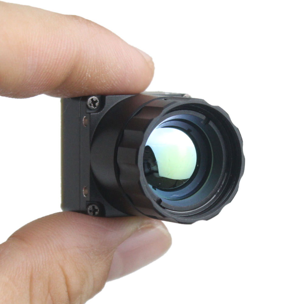
For engineers designing miniature dual-spectrum gimbals for commercial drones and perimeter ground vehicles, check out our detailed technical teardown on the Mini 640 Uncooled LWIR Thermal Camera Module.
3. Industrial Selection Matrix: Noise, Shutter Types, and Interfaces
Picking the ideal vision sensor for factory machinery, defense payloads, or smart infrastructure means balancing pure electro-optical performance against thermal, electrical, and mechanical constraints.
Global Shutter vs. Rolling Shutter Topologies
The choice between global and rolling shutter architectures comes down to a hard trade-off between geometric integrity and raw low-light sensitivity:
- ⚙️ Global Shutter (GS): In a global shutter sensor, every single pixel exposes simultaneously. When the integration window finishes, the accumulated charge is transferred in parallel into an shielded in-pixel analog storage node before column-by-column readout begins. This stops spatial distortion dead in its tracks. GS sensors are mandatory for high-speed automated optical inspection (AOI), fast conveyor sorting, automatic number-plate recognition (ANPR), and drone mapping where target or vehicle speeds exceed 2 m/s. The compromise? Higher silicon complexity, slightly higher read noise, and larger pixel sizes due to the in-pixel storage node.
- ⚙️ Rolling Shutter (RS): Rolling shutter sensors expose and read out the array row by row. If your target or camera moves rapidly during the frame readout cycle, you get severe spatial artifacts (the dreaded "jello effect" or shear distortion). However, because RS pixels need fewer transistors per cell, they offer superior full-well capacity, lower dark current, significantly higher resolutions at attractive price points, and ultra-low read noise (<1.0 e- RMS). RS sensors are ideal for stationary perimeter monitoring, pan-tilt-zoom (PTZ) continuous tracking, and precision radiometric thermography where the platform stays stable relative to the scene.
Interface Selection: High-Speed Embedded vs. Rugged Long-Haul Telemetry
Routing digital video streams from the sensor array to the host processor requires careful electrical interface selection:
- ⚙️ MIPI CSI-2 (Camera Serial Interface): The industry standard for embedded board-level vision. Utilizing low-voltage differential signaling (D-PHY or C-PHY), MIPI CSI-2 transmits raw, uncompressed Bayer or YUV data directly to System-on-Chips (SoCs), FPGAs, and microcontrollers. Trace lengths are typically limited to 10–15 cm on rigid PCBs to maintain signal integrity, making it ideal for compact embedded edge devices. For rapid prototyping and benchtop evaluation of low-bandwidth optical sensors, embedded developers frequently experiment using platforms like Arduino, whereas production industrial systems rely on high-throughput FPGAs and dedicated neural processing units (NPUs).
- ⚙️ GigE Vision / RJ45 Ethernet IP: For factory automation, remote infrastructure, and maritime vision, data must travel over extensive physical distances. Industrial network modules convert raw pixel feeds onboard via dedicated Application-Specific Integrated Circuits (ASICs), compressing video into H.264, H.265, or transmitting uncompressed GigE Vision frames over ruggedized RJ45 or M12 Ethernet lines up to 100 meters without active repeaters. Real-time streaming protocols like RTSP and ONVIF compliance ensure broad interoperability with commercial Video Management Systems (VMS).
- ⚙️ Legacy Analog CVBS: Despite the digital transition, analog Composite Video Blanking and Sync (CVBS) outputs remain widely utilized in defense gimbals, legacy avionics, and low-latency FPV drone links due to its zero-latency, analog signal path.
For deeper procurement analysis and regional compliance standards across European and Asian markets, take a look at our commercial infrared sourcing handbook and our comprehensive engineering review on LWIR camera core selection.
4. Commercial Hardware Comparison: High-Performance Vision & Thermal Modules
Deploying dual-band multi-spectral platforms requires commercial-grade, field-proven hardware cores engineered for SWaP-optimized payloads, thermal stability, and immediate embedded integration. Below is an engineering overview of two industry-standard long-wave infrared modules designed to operate standalone or in tandem with visible CMOS sensor arrays.
1. Uncooled Infrared RJ45 CVBS RTSP IP 640×512 Thermal Sensor Camera Module
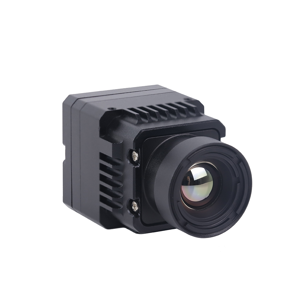
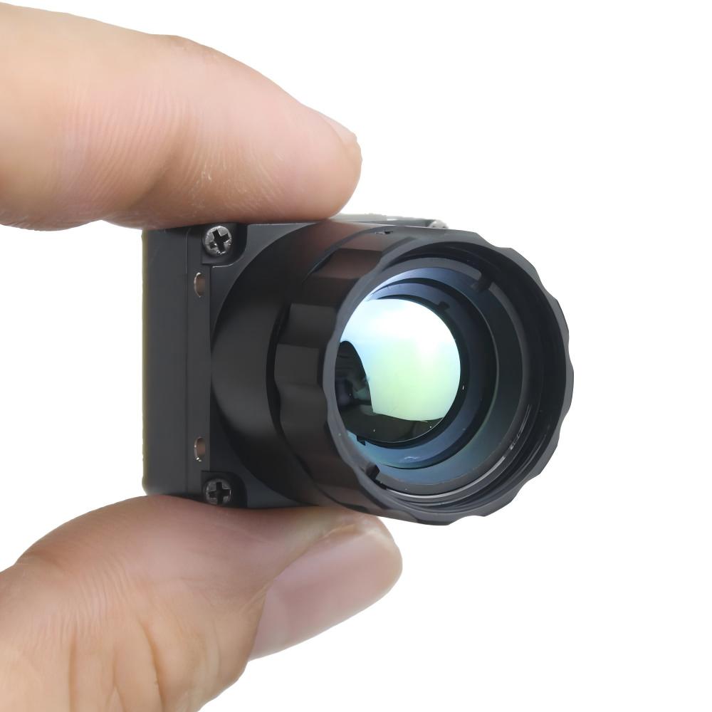
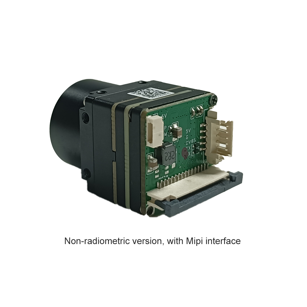
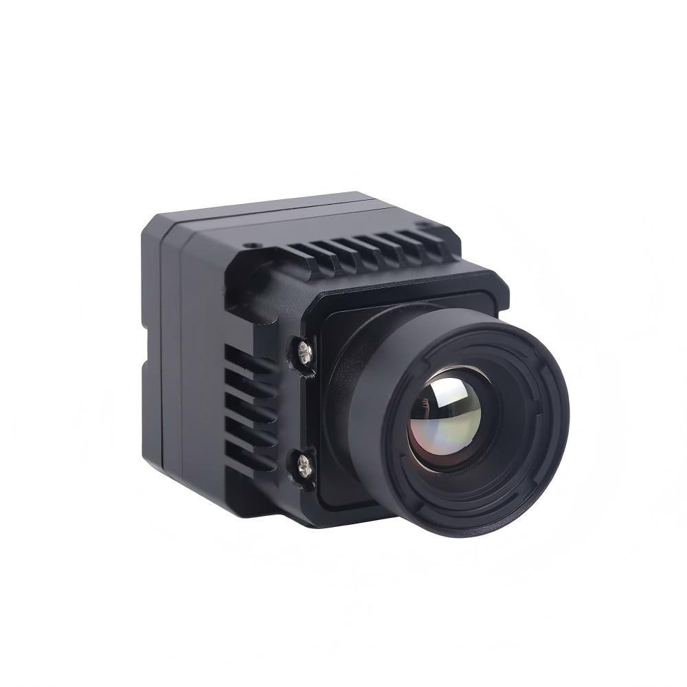
The Uncooled Infrared RJ45 CVBS RTSP IP 640×512 Thermal Sensor Camera Module is an ultra-compact, ASIC-driven thermal imaging engine engineered specifically for small Unmanned Aerial Vehicles (sUAS), tactical drone gimbals, robotic inspections, and perimeter security perimeters. Powered by a high-sensitivity 640×512 VOx microbolometer array with a 12 µm pixel pitch, this module delivers crisp thermal rendering across extreme environmental gradients.
Its hybrid video architecture outputs simultaneous digital IP streams (via RJ45 supporting RTSP/ONVIF protocols with low-latency H.264/H.265 compression) and an uncompressed analog CVBS feed. Its dedicated processing ASIC executes non-uniformity correction (NUC), bad pixel replacement, and digital detail enhancement at the silicon level, offloading compute requirements from the host flight controller or AI computer.
| Specification | Engineering Parameter |
|---|---|
| Detector Type | Uncooled VOx Microbolometer FPA |
| Array Resolution & Pixel Pitch | 640×512 pixels, 12 µm pitch |
| Spectral Response | 8 µm to 14 µm (LWIR) |
| Connectivity & Interfaces | RJ45 (Ethernet IP, RTSP/ONVIF), CVBS Analog |
| Processing Architecture | Dedicated Low-Power ASIC with Hardware DDE & NUC |
| Target Applications | Drone payloads, autonomous robotics, remote security systems |
2. High Resolution Uncooled Infrared 1280×1024 Thermal Imaging LWIR Camera
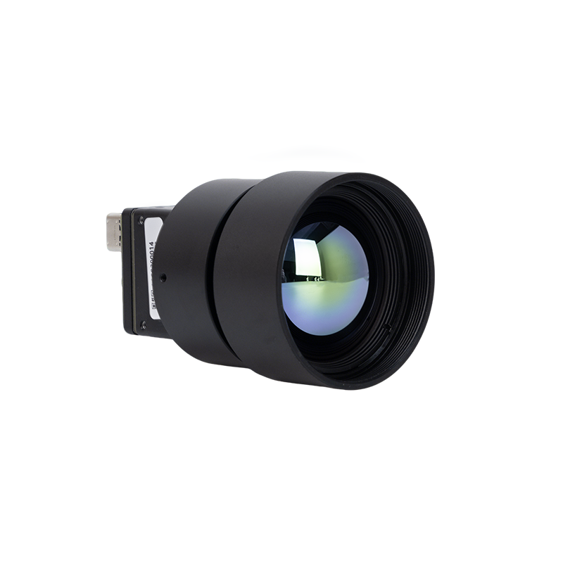
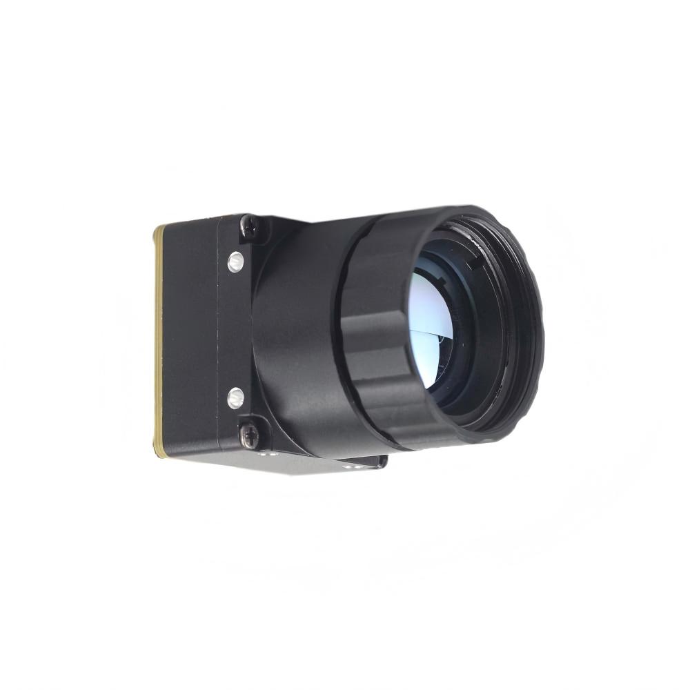
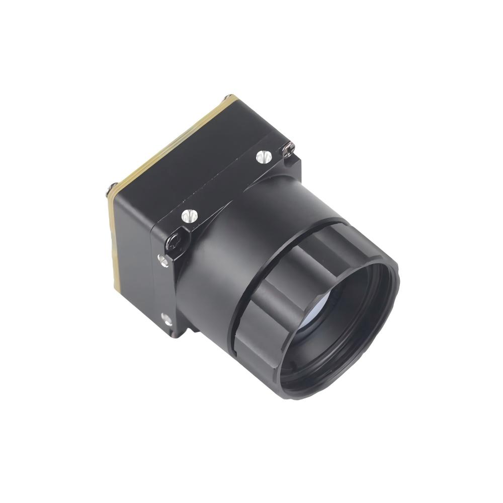
The High Resolution Uncooled Infrared 1280×1024 Thermal Imaging LWIR Camera is a high-grade megapixel radiometric thermal module engineered for high-precision, long-range observation. Featuring an uncooled microbolometer array delivering native SXGA (1280×1024) resolution and integrated with a precision-machined 25mm continuous-focus or fixed optical Germanium lens assembly, this core quadruples the pixel density of standard 640×512 thermal detectors.
Designed for seamless integration into multi-sensor border surveillance turrets, maritime search-and-rescue arrays, and high-accuracy electrical grid diagnostic platforms, this camera core provides high thermal sensitivity (NETD ≤ 40 mK). It delivers clear thermal distinction between minute temperature gradients, ensuring positive target identification at stand-off distances.
| Specification | Engineering Parameter |
|---|---|
| Detector Type | High-Density Uncooled LWIR VOx FPA |
| Array Resolution | 1280×1024 High-Definition Array |
| Integrated Optics | 25mm High-Transmission Germanium Lens Assembly |
| Thermal Sensitivity (NETD) | ≤ 40 mK (@ f/1.0, 300K) |
| Output Options | Digital Parallel / LVDS / Custom Carrier IP Streaming |
| Target Applications | Border observation, maritime navigation, utility infrastructure inspection |
Direct Engineering Comparison
| Architecture Metric | 640×512 RJ45/CVBS Mini Core | 1280×1024 25mm HD Core |
|---|---|---|
| Primary SWaP Focus | Ultra-low weight, minimal volume for micro gimbals | Maximum spatial resolution & detection range |
| Integration Complexity | Plug-and-play Ethernet (RTSP/ONVIF) + Analog | Direct embedded digital bus / high-speed streaming |
| Ideal Visible CMOS Match | 1080p (1920×1080) Global or Rolling Shutter | 4K UHD (3840×2160) Global Shutter Optical Core |
| Radiometric Capabilities | Qualitative thermal tracking + baseline alarms | Full quantitative per-pixel thermographic mapping |
5. Signal Processing, ASIC Deployment, and Latency Optimization
Running high-speed edge AI models (such as YOLOv8/v9 object detectors, multi-target centroid trackers, or real-time segmentation nets) requires a tightly disciplined image pipeline. If you try to push raw, uncompressed high-bit-depth pixel matrices through internal Linux kernel layers and userspace memory queues, you will choke your PCIe bandwidth, spike CPU temperatures, and drop frames constantly.
The Hardware Pre-Processing Chain
Modern industrial cameras offload image cleanup tasks directly to dedicated ASICs or FPGAs before pixel frames ever touch system RAM:
- ⚙️ Non-Uniformity Correction (NUC): Uncooled thermal FPAs drift significantly as the enclosure heats up. The onboard ASIC applies real-time calibration coefficients (gain and offset corrections) gathered during mechanical shutter calibration to equalize drift across every individual microbolometer pixel.
- ⚙️ Digital Detail Enhancement (DDE) & CLAHE: Contrast-Limited Adaptive Histogram Equalization (CLAHE) and custom edge-enhancement filters operate directly on 14-bit raw radiometric inputs. This maps wide dynamic ranges into balanced 8-bit streams while emphasizing low-contrast thermal anomalies against large background temperature signatures.
- ⚙️ Bad Pixel Replacement (BPR): Dead or drifting microbolometer and CMOS pixels are detected in silicon and dynamically patched on the fly using neighborhood spatial interpolation without host processor involvement.
Zero-Copy DMA Pipelines and Glass-to-Glass Latency
When you are designing robotic pick-and-place arms or fast-tracking drone gimbals, "glass-to-glass" latency—the total time from a photon striking the active silicon to the host executing a physical actuator command—must stay below 30 milliseconds. To hit that target, you need zero-copy Direct Memory Access (DMA) architectures:
By routing MIPI CSI-2 or deserialized LVDS signals straight into unified hardware memory shared by the CPU, GPU, and NPU, the operating system avoids expensive memory copies between kernel and user space. The AI engine runs tensor inference directly on the hardware-allocated frame buffer. When integrated with a streamlined ASIC-driven thermal module, dual-band vision pipelines achieve reliable, deterministic 60 fps to 120 fps continuous inference loops without missing a single frame.
6. Frequently Asked Questions (FAQ)
What is the practical difference between CMOS and CCD sensors for embedded industrial vision?
How do you operate a CMOS sensor reliably in electrically noisy industrial environments?
How can B2B buyers source custom CMOS sensors integrated with thermal imaging modules?
📚 References & Further Reading
- Industry Standard: Microbolometer FPA Technology Overview — Wikipedia Microbolometer
- Prototyping Standard: Embedded Sensor Development Platform — Arduino
- Related Guide: Modular Dual-Spectrum Payload Design — Mini 640 Uncooled LWIR Thermal Camera Module Integration
- Commercial Sourcing: Industrial Infrared Core Handbook — Commercial Infrared Sourcing Guide
- Technical Matrix: Choosing the Right Thermal Engine — Thermal Camera Core Selection for Automation