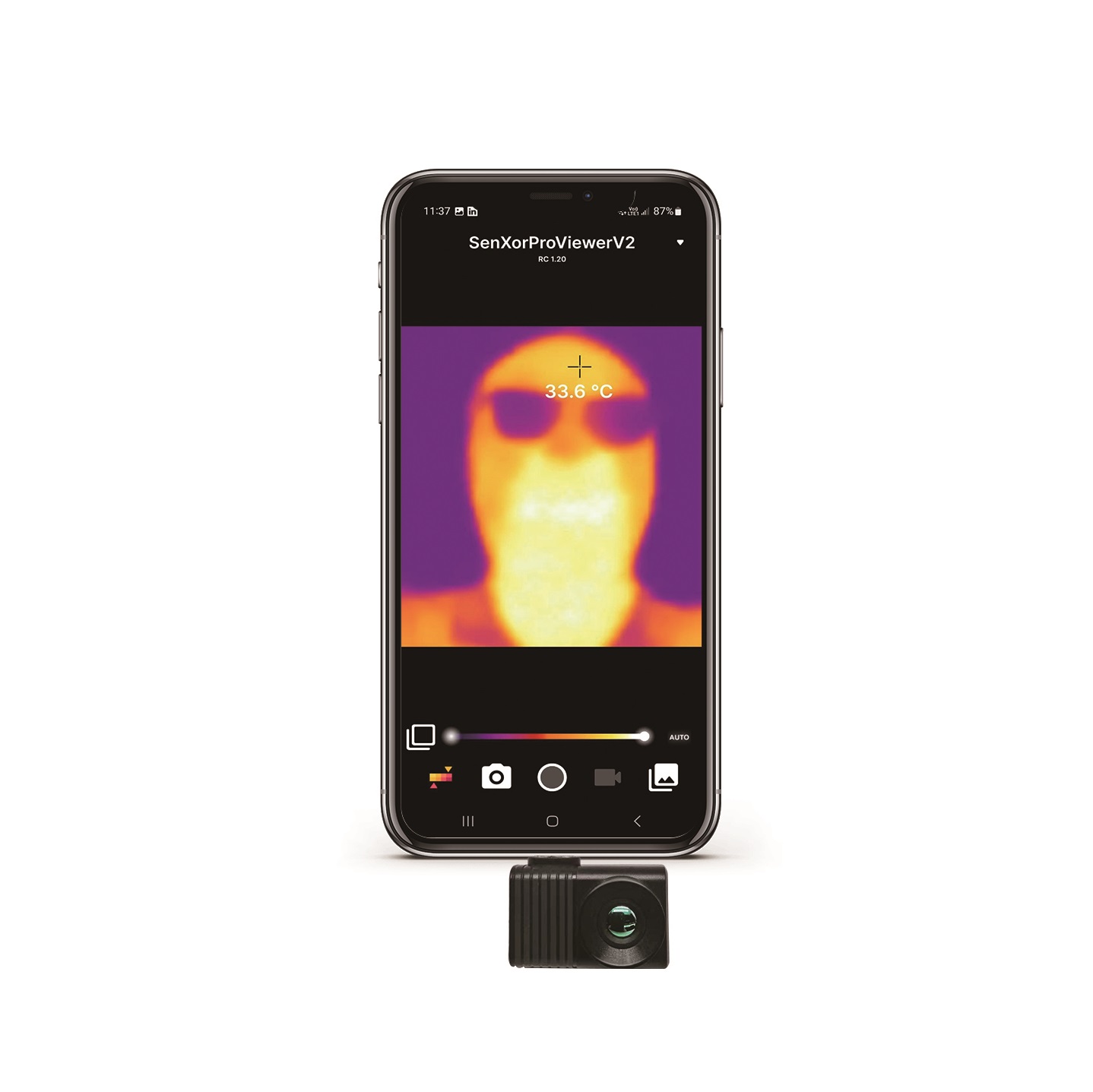
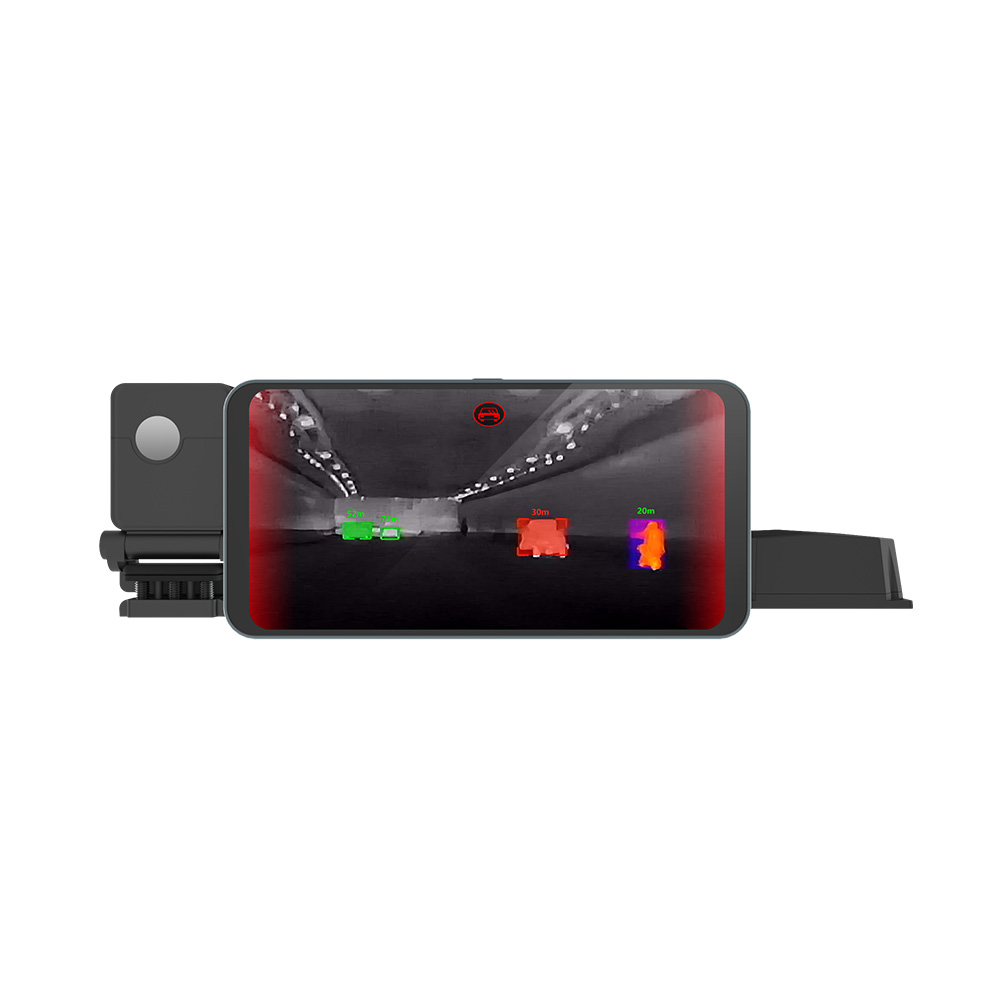


Best Thermal Vision Camera Guide: High-Resolution LWIR & AI Solutions
2026年10月30日
How Does a Thermographic Camera Work? The Complete Tech & Hardware Guide
2026年10月31日
Cheap Thermal Imaging Camera Guide: Stop Buying Blurry Gimmicks (Real 256+ Cores)
The global marketplace for budget thermography is flooded with low-cost consumer gadgets masquerading as diagnostic-grade instruments. Industrial maintenance technicians, facility managers, electrical contractors, and robotic systems integrators regularly fall victim to aggressive marketing campaigns promoting sub-$300 handheld devices or smartphone attachments. These entry-level gadgets boast "high-definition" infrared imaging, yet an inspection of their internal hardware reveals obsolete microbolometer focal plane arrays measuring a mere 32×32 or 80×60 physical pixels. To conceal these severe hardware limitations, manufacturers deploy computational sleights of hand: aggressive bicubic interpolation, bilinear pixel smoothing, or crude edge-blending routines that extract high-contrast visual outlines from a two-dollar visible-light CMOS sensor and lay them over an undefined, low-resolution thermal smear.
In high-consequence industrial diagnostics—such as identifying high-resistance contact points in electrical switchgear, detecting structural moisture saturation beneath commercial roofing membranes, surveying HVAC heat exchangers, or integrating autonomous payloads onto unmanned aerial systems—an interpolated thermal image is dangerous. A mathematical blur cannot distinguish between a dangerous localized phase overload running at 95°C and harmless ambient thermal dissipation around a neutral busbar. When mathematical averaging masks high-temperature thermal gradients, the result is misdiagnosed infrastructure, unnecessary equipment teardowns, missed electrical fault signatures, and elevated risk of catastrophic thermal runaway. Diagnostic precision demands true radiative measurement, not computational guesswork.
To obtain reliable, repeatable thermal performance without paying exorbitant enterprise brand markups, procurement teams and systems engineers must look directly to factory-calibrated, uncooled Long-Wave Infrared (LWIR) OEM camera cores built upon native focal plane arrays of at least 256×192 physical pixels. Diagnostic thermography requires an engineering assessment of key performance parameters: Noise Equivalent Temperature Difference (NETD), optical transmission properties of infrared glass, raw per-pixel radiometric streaming capabilities, and unthrottled real-time refresh rates of 25Hz or higher. By understanding how pixel pitch, sensor lithography, and direct bus integration dictate target acquisition, commercial operators can procure true industrial-grade radiometric vision at a fraction of legacy retail costs. This technical guide exposes deceptive entry-level marketing tactics, details core criteria for evaluating thermal hardware, and showcases bench-tested OEM solutions designed for high-reliability field and airborne integration.
Table of Contents
- 👉 The Cheap Thermal Trap: Native Sensor Arrays vs. Software Upscaling
- 👉 Beyond Megapixels: The Engineering Parameters That Actually Matter
- 👉 Form Factor Showdown: Smartphone Dongles vs. Dedicated Embedded Modules
- 👉 Industrial OEM Specifications: Factory-Direct 256×192 and 640×512 Cores
- 👉 Field Diagnostic Playbook: Electrical, Building Science, and Drone Integration
- 👉 Industrial FAQ: Deep-Dive Technical Clarifications
The Cheap Thermal Trap: Native Sensor Arrays vs. Software Upscaling
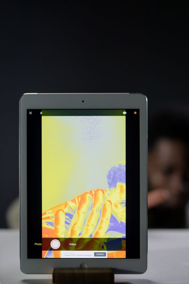
The most widespread deception in the budget thermal imaging sector is the deliberate conflation of display output resolution with native physical focal plane array (FPA) resolution. Consumer-oriented manufacturers regularly emblazon retail packaging, spec sheets, and digital marketing materials with misleading phrases like "Super-IR Resolution," "Ultra-Clarity Enhancement," or "High-Definition Radiometric Display." In almost every case, these descriptors refer strictly to the pixel dimensions of the integrated LCD screen or the software canvas rendered within an accompanying mobile application. Beneath the plastic chassis, the infrared detection engine frequently relies on an entry-level microbolometer array consisting of 4,800 active physical sensor elements configured in an 80×60 matrix, or in some egregious instances, a meager 1,024 elements in a 32×32 grid.
To populate a contemporary screen resolution of 320×240 or 640×480 pixels, the camera's internal image pipeline applies software-level bicubic interpolation, nearest-neighbor upsampling, or edge-enhancement filters derived from an inexpensive visible-spectrum camera module. This computational processing creates the superficial illusion of a clean, structured image by artificially sharpening physical edges and smoothing color gradients across wide swathes of the display. However, this process strips the resulting image of radiometric accuracy. Thermal imaging is not an aesthetic imaging medium; it is a quantitative thermal radiometric measurement science governed by the laws of blackbody radiation, Planck's distribution, and atmospheric transmission windows. When an algorithm calculates nonexistent pixel values between sparse physical measurement points, it introduces artificial mathematical artifacts that directly falsify the radiometric surface temperature map of the target.
Understanding this compromise requires analyzing the physics of microbolometer operation. An uncooled infrared microbolometer operates when incident long-wave infrared radiation (ranging from 8μm to 14μm) strikes a suspended thermal absorption membrane, altering its internal electrical resistance via a specific Temperature Coefficient of Resistance (TCR). This resistance change is measured, amplified, and converted into a digital value via a Read-Out Integrated Circuit (ROIC) layer beneath the micro-bridges. When an 80×60 sensor is focused on an electrical distribution cabinet at a standard working distance of two meters, a single physical microbolometer detector may cover a spatial target area measuring 20×20 millimeters. If an overheating terminal screw or high-resistance lug has a cross-sectional width of only 4 millimeters, that small heat source occupies only a fraction of the physical detector's active surface area.
Under these conditions, the physical sensor averages the high-energy photon flux of the 95°C terminal with the surrounding ambient air and cold metal enclosure panels at 22°C. The single sensor element integrates the total incoming thermal flux across its entire surface, reporting a blended, artificially depressed value—often registering on screen as a non-critical 45°C. When software interpolation processes this blended readout, it broadens the low-temperature blob across adjacent synthetic pixels. The field technician leaves the cabinet in service, unaware that a terminal is approaching ignition. Stepping up to a native 256×192 microbolometer array increases the physical pixel count from 4,800 to 49,152 active detection units. This ten-fold expansion in discrete thermal sensing points slashes the Instantaneous Field of View (IFOV). At the same two-meter distance, the individual 256×192 pixel isolates the 4-millimeter hot spot without diluting its radiative signal across adjacent cold surfaces, capturing the localized temperature spike accurately.
Engineering teams assessing thermal imaging systems can learn more about real microbolometer physics versus consumer-grade interpolations in this Polish industrial infrared camera and sensor technology guide, which contrasts native uncooled sensor arrays with upscaled retail models.
The progression of semiconductor fabrication has enabled uncooled infrared detectors to advance from legacy 17μm and 25μm lithography processes to modern 12μm wafer-level packaging (WLP). A 12μm pixel pitch brings significant advantages to thermal system engineering. By packing individual microbolometer elements closer together, a native 256×192 or 640×512 focal plane array occupies a significantly smaller physical footprint. This reduction in the physical active area of the sensor allows the optical system to shrink proportionately. Because the focal length needed to yield a specific angular field of view decreases as pixel dimensions shrink, the size, thickness, and raw mass of the required Germanium or Chalcogenide glass lenses drop substantially.
Smaller bolometer membranes feature reduced thermal mass, allowing individual pixels to respond more rapidly to thermal flux shifts. Modern 12μm Vanadium Oxide (VOx) detectors exhibit low thermal time constants, typically between 8 and 12 milliseconds, allowing individual pixels to stabilize rapidly without thermal lag. Amorphous Silicon (a-Si) sensors or legacy 25μm bolometers, by contrast, exhibit higher thermal mass and slower thermal response, leading to spatial smearing and ghosting during dynamic panning operations. When evaluating budget-friendly thermal imaging solutions, system architects must look for modern 12μm VOx fabrication nodes rather than liquidated stockpiles of high-mass legacy sensors packaged in updated consumer enclosures.
Beyond Megapixels: The Engineering Parameters That Actually Matter
While native pixel count determines the geometric limits of spatial resolution, resolution alone does not guarantee diagnostic capability. An uncooled Long-Wave Infrared sensor must balance spatial density with thermal sensitivity, radiometric calibration integrity, dynamic response, and optical transmission efficiency. Selecting an industrial-grade thermal imaging core at an economical price point requires careful evaluation of three fundamental technical parameters: Noise Equivalent Temperature Difference (NETD), sensor refresh frequency, and optical transmission engineering.
Thermal sensitivity is quantified through Noise Equivalent Temperature Difference (NETD), expressed in milliKelvins (mK). NETD represents the temperature difference that produces a signal-to-noise ratio of unity within the detector circuitry; it establishes the minimum thermal contrast a camera can resolve above its own electrical noise floor. In sub-$300 consumer units, NETD values frequently exceed 70mK to 100mK. Under these conditions, the sensor struggles to differentiate subtle thermal gradients from internal electronic noise. Scanning a low-contrast target, such as an insulated building envelope on an overcast day or a composite wind turbine blade, yields an image marred by heavy fixed-pattern noise (FPN) and thermal noise patterns. Structural anomalies, subterranean moisture paths, and small insulation voids disappear within the sensor's baseline noise floor.
High-performance industrial cores achieve NETD ratings of less than 40mK to 50mK, with top-tier VOx sensors reaching sensitivities below 35mK. An NETD of 40mK allows the camera to cleanly resolve temperature deltas as fine as 0.04°C. Subtle heat transfer variations—such as convective air drafts through electrical conduits, early-stage moisture evaporation beneath single-ply commercial roofs, or slight friction variations in conveyor bearings—stand out with clean contrast. When reviewing thermal core datasheets, ensure the NETD rating specifies an aperture of f/1.0 at an ambient operating temperature of 300K (27°C). Manufacturers of budget consumer hardware frequently obscure poor sensitivity by citing theoretical modeling calculations, post-processed software noise-filtering values, or simulated apertures that do not reflect actual real-world bench conditions.
The temporal refresh rate of an infrared camera module determines its utility in dynamic field inspections. Under international dual-use export regulations, including the Wassenaar Arrangement and U.S. ITAR guidelines, thermal imaging devices operating at refresh rates of 9Hz or greater have historically faced stringent cross-border export restrictions. To navigate these regulatory hurdles without maintaining regional compliance infrastructure, many budget camera manufacturers lock their hardware outputs to a sluggish 8.7Hz or 9Hz frame rate.
A 9Hz refresh rate introduces severe limitations during industrial diagnostics. When an operator pans a 9Hz camera across an electrical enclosure, the sensor displays noticeable latency, frame lag, and motion blur. If the camera moves faster than the slow refresh cycle can process, high-temperature transients are missed, and spatial borders between terminals blur into neighboring panels. In aerial drone integrations, an 8.7Hz sensor is largely ineffective: flight speeds between 5 and 12 meters per second smear the ground footprint across frames, preventing companion computers from executing automated edge-AI target tracking, object detection, or thermal mapping algorithms.
Dynamic platform integrations require continuous, unthrottled 25Hz, 30Hz, or 50Hz video streaming. A 25Hz to 50Hz frame rate delivers smooth visual tracking, eliminates motion blur, and ensures that the ROIC captures transient thermal spikes as electrical switchgear is switched under varying loads. Integrators building automated inspection platforms or UAV sensor pods can reference this technical guide on LWIR thermal imaging camera modules and mini cores for edge AI and UAVs, which outlines the hardware requirements for pairing high-speed infrared acquisition with embedded processing architectures.
The optical system of an infrared camera requires equal engineering scrutiny. Standard optical glasses, such as fused silica, borosilicate, or optical crowns, are opaque within the 8μm to 14μm LWIR spectrum. Therefore, thermal camera lenses must be constructed from specialized materials capable of transmitting long-wave infrared radiation without excessive absorption or scattering losses. The industry standard material is single-crystal Germanium (Ge). Germanium features an exceptionally high refractive index of approximately 4.0, which allows optical designers to engineer compact, high-power lenses with minimal spherical aberrations. However, Germanium is dense, supply-constrained, expensive to diamond-turn, and subject to thermal runaway: at temperatures above 100°C, its internal free electron density climbs rapidly, causing transmission to drop.
To deliver high optical performance at budget-friendly price points, leading thermal optics manufacturers utilize precision-molded Chalcogenide glass compounds. Chalcogenide materials—synthesized from chemical matrices of germanium, arsenic, selenium, and tellurium—can be hot-pressed and molded into complex aspheric lens geometries, significantly reducing per-unit manufacturing costs compared to traditional diamond-turned Germanium optics. Companies such as LightPath Technologies design precision-molded Chalcogenide optical systems that provide high transmission across the 8μm to 14μm band while maintaining lower thermal focal drift (dn/dT) than pure Germanium across shifting ambient temperatures. Integrating an aspheric Chalcogenide optical element with a wide f/1.0 or f/1.1 aperture ensures the focal plane array captures maximum photon flux, allowing the underlying microbolometer to achieve its optimal NETD performance in demanding environments.
Form Factor Showdown: Smartphone Dongles vs. Dedicated Embedded Modules
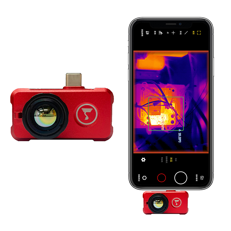
When selecting an economical thermal imaging system, systems engineers, project managers, and field technicians face a fundamental architectural choice: should they deploy consumer smartphone attachments (USB-C or Lightning dongles) or integrate dedicated uncooled OEM thermal camera modules? While smartphone attachments dominate the sub-$400 consumer retail space, their mechanical, thermal, and software characteristics introduce operational challenges in sustained commercial environments.
Smartphone thermal accessories rely entirely on the host phone's internal processor, touch display, and battery. While this reduces initial purchase costs by eliminating the need for a dedicated display and processing unit, it creates several operational trade-offs in commercial settings:
- ⚠️ Mechanical Interface Vulnerabilities: In smartphone accessories, the male USB-C or Lightning connector bears the physical load of the sensor module. In active industrial environments, minor accidental bumps, drops, or continuous mechanical vibration can strain or snap the physical connector. This risk is amplified when working inside high-voltage electrical cabinets or operating near moving machinery, where a dropped or broken accessory can damage both the sensor and the host mobile device.
- ⚠️ Host OS Latency and Process Throttling: Consumer mobile operating systems (Android and iOS) are not built for deterministic real-time data acquisition. Background processes, automatic app updates, incoming calls, and dynamic processor throttling can interrupt the camera app. Users frequently report thermal frame freezes, app crashes, and dropped video frames during data-logging sessions, making long-term continuous thermal monitoring unreliable.
- ⚠️ Conductive and Radiative Thermal Contamination: Modern high-performance smartphones generate significant internal heat across their processor packages, 5G modems, and fast-charging battery packs. This heat dissipates outward through the phone chassis. Because a smartphone dongle is plugged directly into the phone's base, heat from the phone body radiates directly onto the thermal camera housing, interfering with the internal temperature sensors used for shutterless flat-field correction (NUC) and biasing radiometric calculations.
- ⚠️ Battery Drain and Port Wear: Thermal camera modules continuously power a microbolometer array, an active Read-Out Integrated Circuit, and an onboard Image Signal Processor (ISP), drawing steady current from the smartphone's battery. This active draw limits practical field inspections to 60 to 90 minutes before the phone battery is exhausted. Continuous charging and discharging cycles also degrade the host device's battery life over time.
Dedicated uncooled OEM thermal camera modules, by contrast, are engineered for rugged mechanical mounting, low-power continuous operation, and predictable system integration. These bare-board or enclosed modules provide direct hardware communication buses—such as MIPI CSI-2, DVP parallel video, SPI, and native USB video class (UVC) pipelines—allowing them to integrate into custom industrial enclosures, drone gimbals, robotic systems, and continuous monitoring arrays.
The high bandwidth of the MIPI CSI-2 (Camera Serial Interface-2) standard enables raw 14-bit or 16-bit radiometric sensor data to feed directly into the hardware ISP of embedded system-on-chip (SoC) architectures (such as NVIDIA Jetson Orin, Rockchip RK3588, or Raspberry Pi CM4). This direct connection bypasses the latency, packet encapsulation overhead, and bus contention common to consumer USB connections. System architects can also utilize parallel digital video ports (DVP) to pipe raw sensor streams into low-power field-programmable gate arrays (FPGAs) or custom microcontrollers, including embedded vision processing hardware from JM Chip, enabling automated, sub-millisecond edge analysis, thermal threshold alarms, and closed-loop process automation.
Industrial OEM Specifications: Factory-Direct 256×192 and 640×512 Cores
By moving past consumer retail products and sourcing factory-calibrated OEM modules directly, industrial teams can secure uncooled LWIR cores that provide uncompromised native resolutions, standard frame rates, and calibrated radiometric output at accessible price points. The two modules highlighted below illustrate the hardware performance accessible to system designers when eliminating brand overhead, retail distribution markups, and consumer packaging.
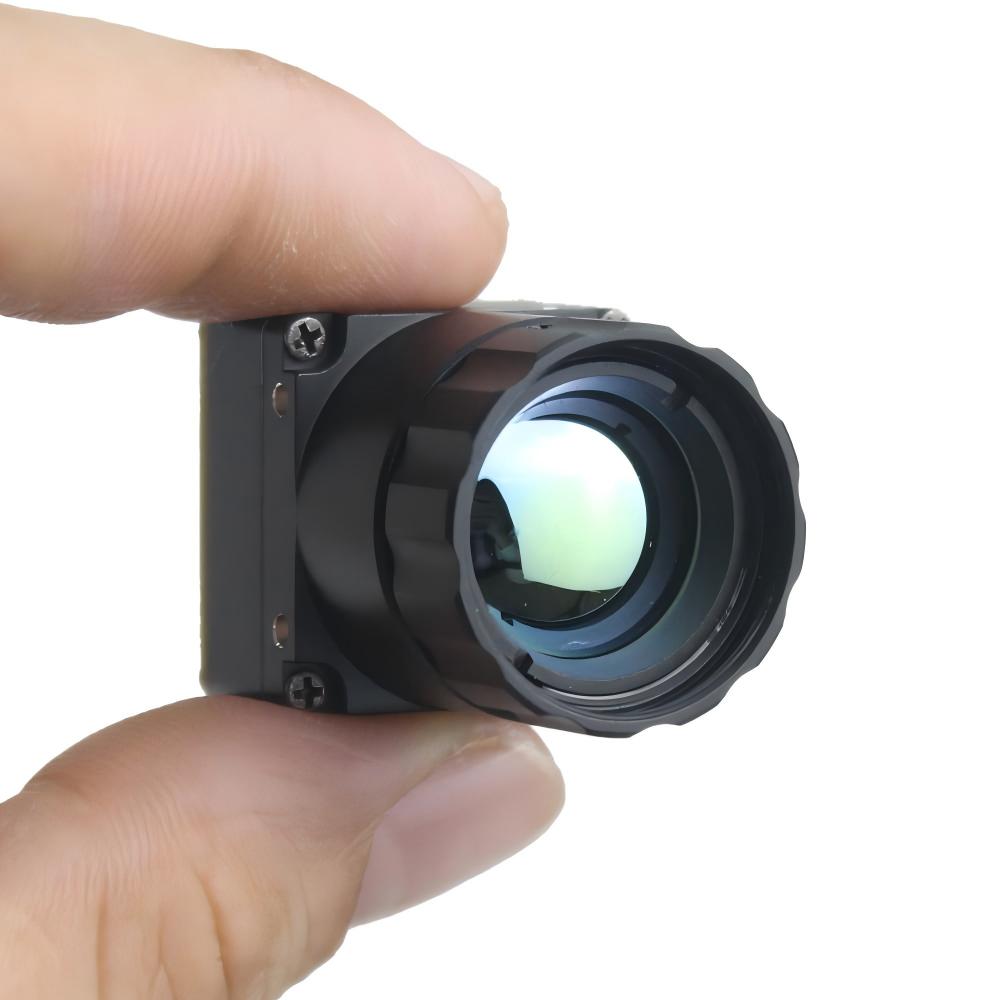
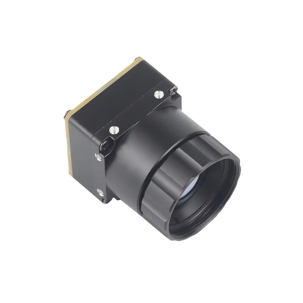
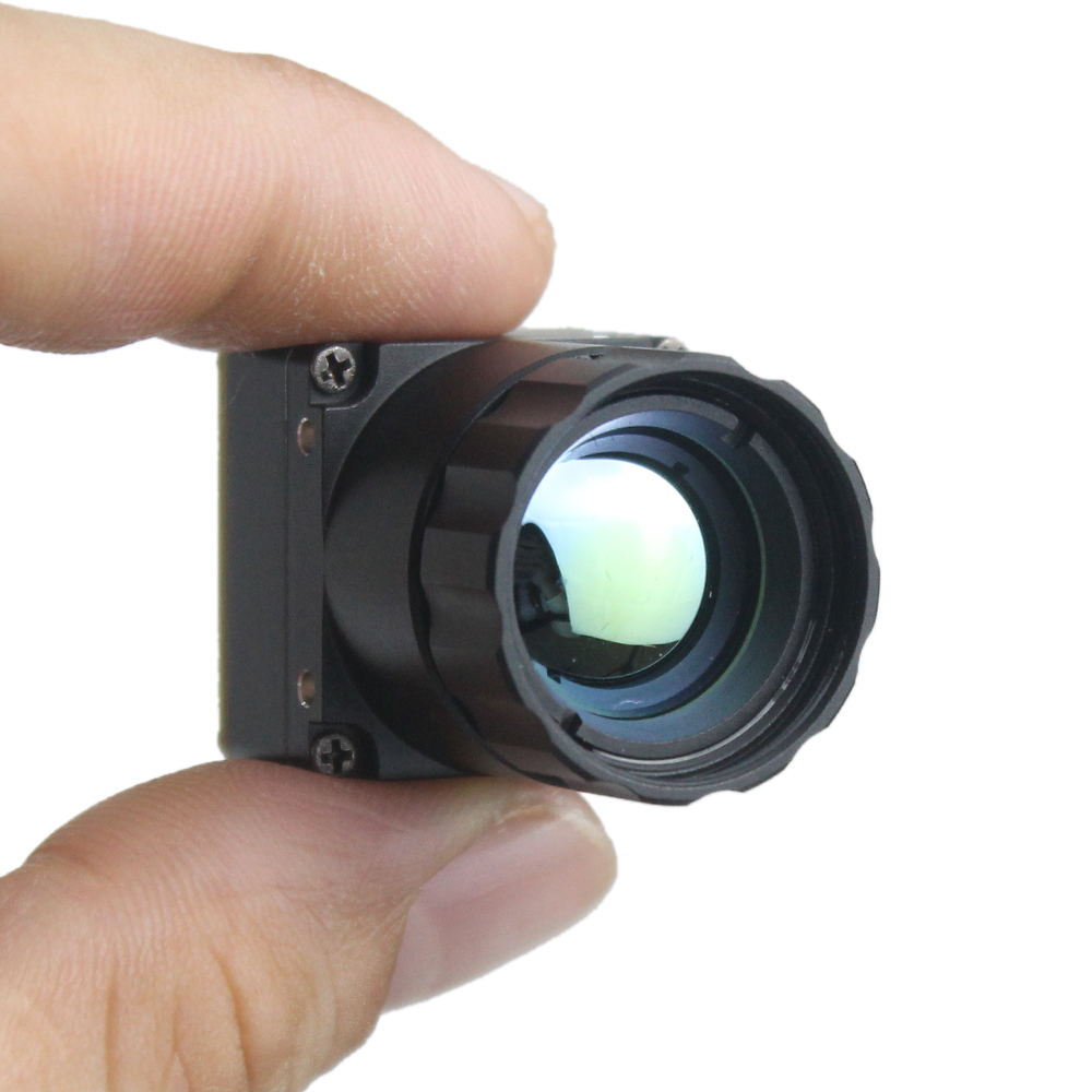
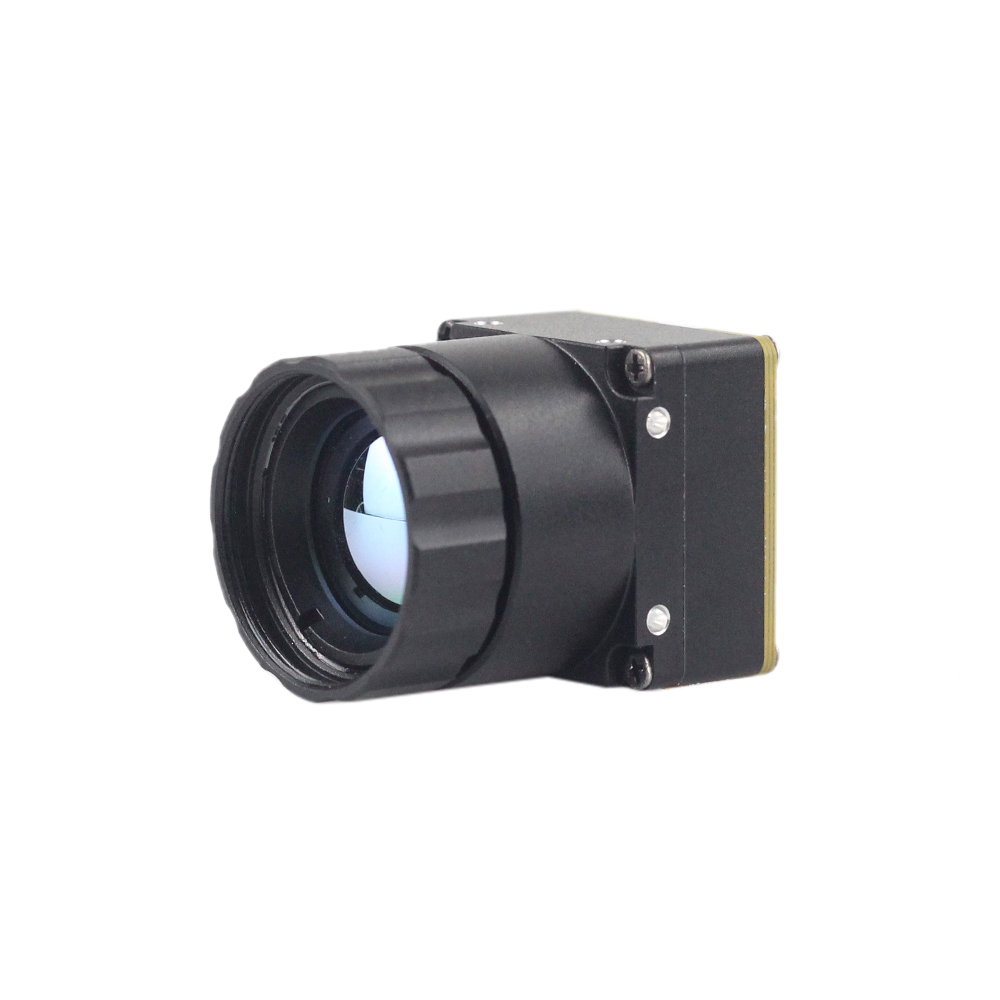
Mini 256 Uncooled LWIR Thermal Camera Module
The Mini 256 Uncooled LWIR Thermal Camera Module delivers high-precision radiometric thermal imaging in a compact, low-SWaP (Size, Weight, Power) configuration. Engineered around an uncooled Vanadium Oxide (VOx) focal plane array, this core provides a native resolution of 256×192 physical pixels at a modern 12μm pitch. Designed for industrial monitoring stations, robotic platforms, automated production sweeps, and demining payloads, the module outputs real-time, uniform thermal imagery backed by full-frame radiometric data.
Mini 256 Uncooled LWIR thermal Camera Module adopts high-performance infrared detectors for ultra-clear thermal imaging and accurate temperature measurement. It captures infrared radiation and outputs a uniform thermal image with radiometry.
View Product Details & Pricing ➔
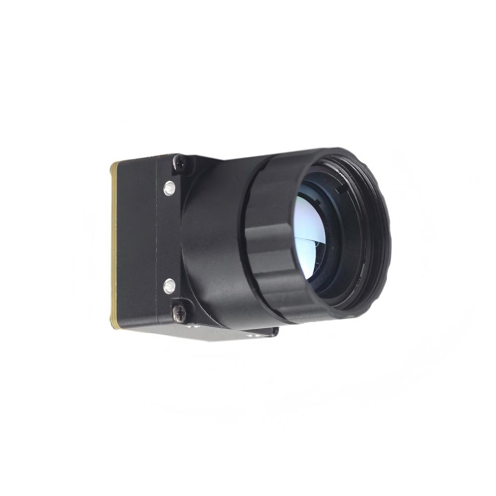
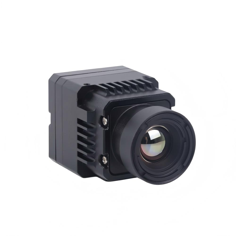
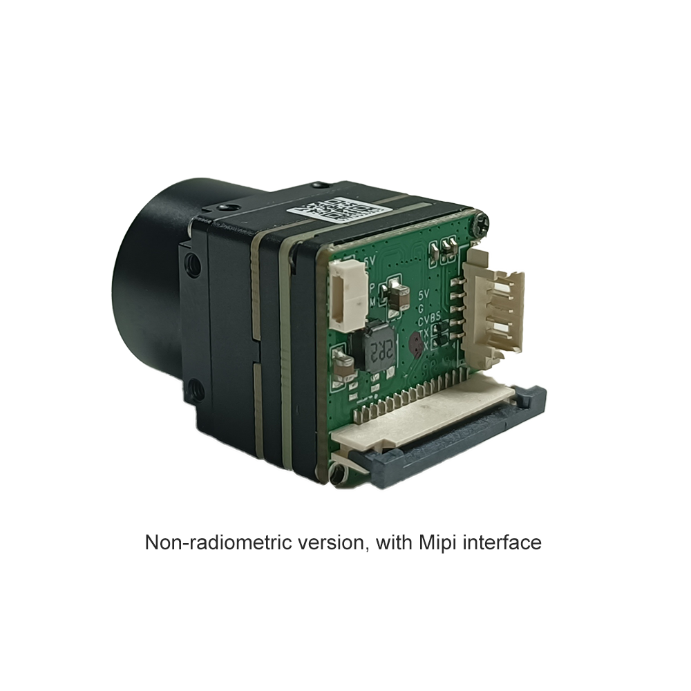
Mini2 640×512 9mm Thermal Imaging Camera Module For Drones
For applications requiring extended standoff distances, wide-area spatial coverage, or integration into autonomous aerial vehicles, the Mini2 640×512 9mm Thermal Imaging Camera Module expands detector density to 327,680 discrete physical measurement pixels. Equipped with a direct MIPI CSI-2 interface and an athermalized 9mm optical assembly, this module transmits low-latency, high-resolution thermal streams directly to onboard computing platforms for automated aerial mapping, edge-AI object detection, and infrastructure inspection.
Uncooled Infrared Mini2 640x512 9mm Thermal Imaging Camera Module For Drones, Mini uncooled infrared thermal imaging module features in sharp and crisp image presentation, compact size and low cost.
View Product Details & Pricing ➔
Comprehensive Engineering Hardware Matrix
The table below provides a detailed technical comparison between the factory-calibrated Mini 256 core, the high-resolution Mini2 640 drone module, and the typical specifications found in low-cost consumer thermal imaging accessories:
| Specification / Parameter | Mini 256 Uncooled LWIR Module | Mini2 640×512 9mm Drone Module | Typical Cheap Consumer Benchmark |
|---|---|---|---|
| Native Array Resolution | 256×192 pixels (49,152 active points) | 640×512 pixels (327,680 active points) | 80×60 to 160×120 (Interpolated to 640×480) |
| Detector Architecture | Uncooled Vanadium Oxide (VOx) | Uncooled Vanadium Oxide (VOx) | Amorphous Silicon (a-Si) / Legacy VOx |
| Pixel Pitch | 12μm lithography node | 12μm lithography node | 17μm to 25μm legacy nodes |
| Spectral Operational Band | 8μm – 14μm (LWIR) | 8μm – 14μm (LWIR) | 8μm – 14μm (Unfiltered) |
| Thermal Sensitivity (NETD) | < 40mK to 50mK (@ f/1.0, 300K) | < 40mK (@ f/1.0, 300K) | > 70mK to 150mK |
| Native Frame Refresh Rate | 25Hz / 30Hz Fluid Video | 25Hz / 30Hz / 50Hz Dynamic Video | 8.7Hz to 9Hz (Export Capped) |
| Primary Hardware Interfaces | USB 2.0 / DVP / UART Radiometric Bus | Direct MIPI CSI-2 / USB / DVP | Proprietary Mobile USB-C / Lightning |
| Radiometric Data Integrity | Full-frame calibrated per-pixel matrix | Full-frame calibrated per-pixel matrix | Single-spot estimate / RGB color mapping |
| Optical Integration | Integrated Athermalized Prime Lens | 9mm Precision Athermalized Lens | Molded low-aperture hybrid lens |
| Measurement Accuracy | ±2°C or ±2% of reading | ±2°C or ±2% of reading | ±3°C to ±5°C (High Drift) |
| System Mass | Ultra-low weight (<20g) | Low-SWaP optimized (<30g) | 35g – 70g (Chassis dependent) |
For cross-border defense, perimeter security, and harsh industrial surveillance designs, engineers can consult this Arabic guide on 25Hz LWIR camera modules for defense and industrial monitoring, which examines long-wave infrared integration under elevated ambient temperature conditions.
Field Diagnostic Playbook: Electrical, Building Science, and Drone Integration
Selecting an infrared imaging core with a native 256×192 or 640×512 resolution and an NETD under 40mK provides quantifiable diagnostic advantages across field inspections. Below is an overview of how sensor resolution, thermal sensitivity, and optical performance impact three common industrial inspection workflows.
1. High-Voltage Electrical Diagnostics and Switchgear Inspection
Electrical failures are almost invariably preceded by elevated resistive heating. Micro-corrosion, oxidation, improper torque on terminal screws, and phase load imbalances generate localized heat signatures. Using a low-resolution (80×60) thermal camera presents real diagnostic risks:
- ⚠️ The Distance-to-Spot Ratio (D:S) Problem: To achieve accurate temperature readings with an 80×60 core, the technician must stand dangerously close to energized conductors, often within arc-flash boundary zones. If the technician maintains a safe working distance of two to three meters, the sensor's Instantaneous Field of View averages the small terminal's heat across adjacent cold surfaces, under-reporting hot spots by tens of degrees Celsius.
- ✅ The 256×192 Solution: A native 256×192 uncooled core with a 12μm pitch provides a tighter IFOV, allowing the technician to resolve individual phase lugs, busbar joints, and knife switches from well outside the flash boundary. The camera's full-frame radiometric output streams directly to diagnostic software, catching subtle 3°C to 5°C relative temperature rises long before insulation degradation or terminal failure occurs.
2. Building Envelopes, Insulation Diagnostics, and Moisture Tracing
Building diagnostics and roofing inspections require high thermal sensitivity, as temperature differentials across insulation voids, structural air infiltration paths, and wet sub-membrane assemblies rarely exceed 1.0°C to 2.0°C.
- ⚠️ The Sensitivity Bottleneck: Cheap consumer thermal devices with high NETD values (>80mK) cannot differentiate subtle temperature shifts from their own internal electronic noise. Evaporative cooling from moisture leaks appears as an indistinct, noisy area on screen, making it difficult to trace the water boundary.
- ✅ The Sub-40mK Advantage: Deploying a core with an NETD of <40mK cleanly visualizes subtle thermal boundaries. Evaporative cooling beneath built-up roofing membranes produces distinct, high-contrast thermal patterns. In building envelope inspections, stud framing, settling wall insulation, and air leaks around fenestration stand out clearly, enabling fast and accurate structural assessments.
3. Autonomous Drone Payloads: Utility Solar and Pipeline Monitoring
Airborne inspections of utility-scale photovoltaic (PV) installations and municipal distribution pipelines demand high pixel counts and standard video frame rates.
- ⚠️ The Drawbacks of 9Hz Consumer Attachments: Panning a 9Hz thermal camera from a drone moving at 6 to 10 m/s causes severe motion blur and dropped frames. Smeared thermal images prevent companion computers from detecting defective bypass diodes, cracked solar cells, or pressurized pipeline leaks.
- ⚙️ The 640×512 MIPI Advantage: Integrating a 640×512 uncooled thermal core via direct MIPI CSI-2 bus directly into an onboard processing unit (such as an NVIDIA Jetson module) enables smooth 25Hz to 50Hz imaging. Operating at altitudes of 40 to 60 meters, the aerial platform covers large solar arrays in a single battery cycle, running onboard edge-AI models to identify and geotag defective photovoltaic cells in real time.
Industrial FAQ: Deep-Dive Technical Clarifications
Are thermal cameras in the $200-$400 price range actually worth buying for home or electrical inspection?
Why are smartphone-attached cheap thermal cameras often frustrating to use in the field?
What is the most critical specification to verify before purchasing a budget thermal camera?
Architectural Synthesis: Avoiding the Cheap Trap
Procuring a dependable, high-resolution thermal imaging camera does not require spending thousands of dollars on enterprise handheld brands. The high prices of traditional commercial thermal devices are primarily driven by corporate brand overhead, complex distribution channels, and retail consumer packaging. By focusing directly on factory-calibrated OEM uncooled Long-Wave Infrared (LWIR) cores featuring true 256×192 or 640×512 detector arrays, modern 12μm pixel pitch, low NETD values (<40mK), and robust integration buses like MIPI CSI-2 and DVP, system designers and engineers can deploy true industrial-grade radiometric tools while keeping costs accessible. Choosing factory-direct OEM modules ensures your diagnostic workflows are supported by true physical sensor performance, reliable optics, and verifiable radiometric measurements.
📚 References & Further Reading
- Industry Standard: Precision Infrared Optical Materials & Chalcogenide Fabrication: LightPath Technologies
- Industry Standard: Embedded Digital Video Processors and Sensor Interfacing: JM Chip
- Related Guide: Uncooled LWIR Thermal Imaging Modules and Mini Cores for Edge AI & UAV Payloads: Thermal-Image.com Core Integration Guide
- Related Guide: Infrared Camera Sensor Physics and Native Industrial Resolution Standards: Polish Industrial Sensor Evaluation
- Related Guide: 25Hz Long-Wave Infrared Camera Integration for Defense and Harsh Industrial Environments: Arabic LWIR 25Hz Surveillance Guide