
Thermal Infrared Camera Guide: Working Principles, Resolution & Industrial Selection
2026年10月31日
Infrared Camera Thermal Modules: The Ultimate Industrial & OEM Selection Guide
2026年11月13日

Compact Thermal Imaging Camera: OEM Selection Guide for Drones & Micro-Inspection
Integrating thermal vision into ultra-constrained mechanical platforms requires balancing optical physics against size, weight, power, and cost (SWaP-C). Whether designing a sub-250g reconnaissance drone that must comply with strict civil aviation categories or engineering an automated optical inspection (AOI) bench capable of identifying hairline micro-shorts on densely populated printed circuit boards (PCBs), selecting the right compact thermal imaging camera core dictates your product's performance ceiling. In both domains, legacy thermal cores—burdened by hefty germanium optics, power-hungry focal plane arrays (FPAs), and bulky aluminum enclosures—are obsolete.
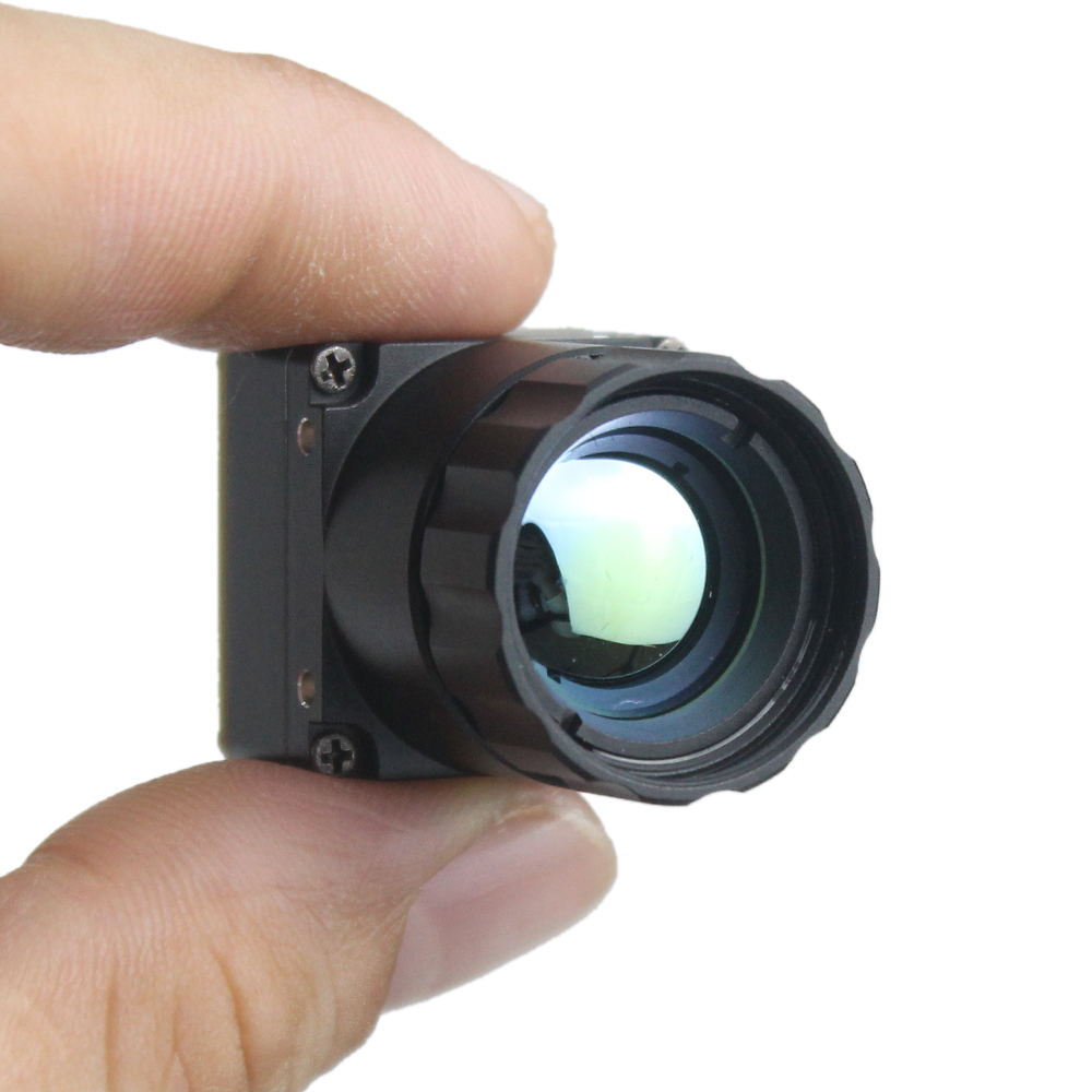
Modern original equipment manufacturers (OEMs) demand uncooled long-wave infrared (LWIR) cores that deliver factory-calibrated radiometry, sub-40mK thermal sensitivity, and native MIPI CSI-2 or USB interfaces within a footprint barely exceeding the size of a postage stamp. This definitive engineering guide dissects the architectural, optical, electrical, and radiometric criteria necessary to evaluate, integrate, and deploy a compact thermal imaging camera into advanced airborne payloads and high-precision micro-inspection systems.
Table of Contents
- 👉 1. Engineering Physics of Miniaturized LWIR Sensors
- 👉 2. SWaP-C Constraints in Airborne & Robotic Integration
- 👉 3. Optical Engineering: Lens Materials, IFOV, and Working Distance
- 👉 4. Hardware Interfaces, Signal Pipelines, and Edge Computing
- 👉 5. Radiometric Processing vs. Qualitative Thermography
- 👉 6. OEM Benchmark: Mini 256 vs. Mini2 640 Product Comparison
- 👉 7. Application Blueprints: Sub-250g Drones vs. Micro-Inspection Benches
- 👉 8. Thermal Drift, In-Flight Calibration, and Environmental Hardening
- 👉 9. Frequently Asked Questions (FAQ)
1. Engineering Physics of Miniaturized LWIR Sensors
At the physical core of every modern compact thermal imaging camera lies an uncooled microbolometer focal plane array (FPA). Unlike cooled medium-wave infrared (MWIR) or short-wave infrared (SWIR) sensors that require cryogenic Stirling cycle mechanical coolers operating at liquid nitrogen temperatures (77 Kelvin), uncooled LWIR detectors capture radiation entirely within the 8 µm to 14 µm atmospheric transmission window using thermally isolated, suspended thin-film microstructures operating at ambient temperature.
Incoming infrared photons pass through an antireflective-coated objective lens and strike tiny suspended pixel membranes inside a vacuum-sealed cavity. Each microscopic pixel absorber absorbs the incident photon energy, causing an instantaneous micro-Kelvin increase in its localized lattice temperature. This thermal shift triggers a measurable change in electrical resistance within the detector material, which an underlying CMOS Readout Integrated Circuit (ROIC) samples, digitizes via on-chip analog-to-digital converters (ADCs), and translates into a serialized stream of digital counts.
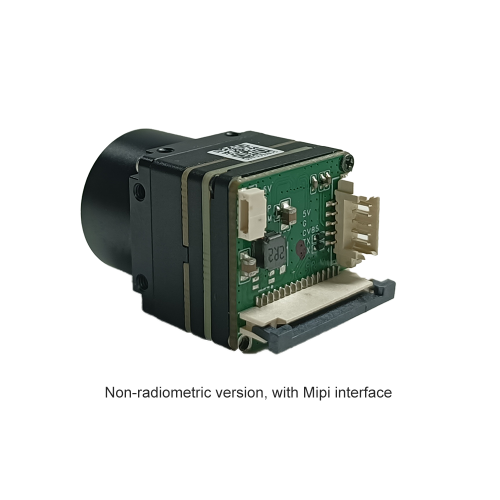
Vanadium Oxide (VOx) vs. Amorphous Silicon (a-Si)
Miniaturized thermal engines rely almost exclusively on either Vanadium Oxide (VOx) or Amorphous Silicon (a-Si) thin-film resistor materials. For size-, weight-, and performance-critical OEM payloads, VOx remains the unchallenged aerospace and industrial benchmark due to several core material characteristics:
- ✅ Temperature Coefficient of Resistance (TCR): VOx demonstrates an exceptionally high TCR of approximately -2% to -3% per Kelvin at ambient operational temperatures, compared to roughly -1.5% to -2.5% per Kelvin for a-Si. This elevated TCR produces a wider dynamic signal swing across the ROIC columns for every millikelvin of target temperature variance, enabling higher signal-to-noise ratios (SNR).
- ✅ 1/f Flicker Noise Floor: VOx thin films possess a substantially lower low-frequency flicker (1/f) noise profile than a-Si lattices. This noise advantage allows the microbolometer to register minute thermal gradients without requiring aggressive temporal filtering algorithms that introduce motion blur or smearing artifacts during rapid flight maneuvers or high-speed board scanning.
- ✅ Vacuum Packaging Scalability: Wafer-Level Packaging (WLP) techniques for VOx allow microscopic silicon or metal cavities to be evacuated and hermetically sealed directly at the semiconductor wafer scale. By capping the microbolometer die with an antireflection-coated silicon window under high vacuum, WLP completely eliminates the heavy, bulky ceramic-metal vacuum enclosures historically needed for thermal sensors, reducing raw sensor die mass down to single-digit grams.
Pixel Pitch Scaling and Diffraction Limitations
Over the past two decades, uncooled microbolometers evolved from 25 µm and 17 µm pixel pitches down to modern 12 µm architectures, with 10 µm variants entering prototype production. In compact thermal imaging systems, shrinking pixel pitch yields dramatic SWaP-C advantages. A 12 µm 640×512 detector array occupies an active area of only 7.68 mm × 6.14 mm. By reducing the physical footprint of the active image plane, the optical focal length required to achieve an identical angular field of view (FOV) scales down proportionately. Smaller focal lengths translate directly into smaller lens diameters, thinner optic profiles, and an exponential drop in optical glass mass.
However, physics imposes fundamental boundaries as pixel dimensions approach the 12 µm mark. The long-wave infrared spectrum spans wavelengths from 8 µm to 14 µm, with a nominal central wavelength ($\lambda$) around 10 µm. When the pixel pitch ($p = 12\ \mu\text{m}$) approaches the wavelength of the imaged radiation, diffraction effects become dominant. The radius of the central Airy disk spot produced by diffraction through a circular aperture is governed by the Abbe diffraction formula:
rAiry = 1.22 × λ × f/#
For an ultra-fast optical system with an aperture of f/1.0 imaging at λ = 10 μm, the radius of the central Airy disk is 12.2 µm, yielding a full Airy spot diameter of 24.4 µm. This spot size spans approximately two full pixels on a 12 µm detector. If an optical designer attempts to curb payload size by stopping down to a slower f/1.4 or f/1.6 lens, the Airy disk expands to over 34 µm, spanning nearly three pixels and causing spatial blurring that degrades the sensor's Modulation Transfer Function (MTF). Consequently, modern compact LWIR cores demand fast optical architectures (typically f/1.0 to f/1.1) engineered with minimal optical aberrations to preserve the resolving power of 12 µm pixels.
Thermal Sensitivity (NETD) and Signal-to-Noise Ratio
Noise Equivalent Temperature Difference (NETD) defines the fundamental thermal resolution metric of an infrared sensor. Measured in milliKelvins (mK), NETD represents the target temperature difference that produces a signal-to-noise ratio of unity at the output of the ROIC when viewing a uniform blackbody target. The governing relationship of microbolometer NETD is defined by:
NETD = (4 × f/#2 × Vn) / (τopt × Adet × Rv × (ΔP / ΔT))
Where Vn is the root-mean-square electrical noise voltage, τopt is the optical transmission efficiency of the lens assembly, Adet is the active pixel surface area, Rv is the responsivity of the microbolometer, and (ΔP / ΔT) is the rate of change of emitted blackbody radiative power with respect to temperature across the 8–14 µm spectral window.
A compact thermal imaging camera delivering an NETD ≤ 40 mK can resolve minute thermal shifts down to 0.04°C. In printed circuit board micro-inspection, this level of sensitivity distinguishes micro-watt thermal dissipations on sub-millimeter integrated circuit traces before destructive electrical shorts occur. In airborne operations, an NETD below 40 mK ensures clear detection across uniform natural landscapes where background vegetation, soil, and bedrock exhibit near-identical bulk temperatures.
2. SWaP-C Constraints in Airborne & Robotic Integration
Designing mobile airborne systems and compact robotic inspection probes requires continuous optimization of Size, Weight, Power, and Cost (SWaP-C). In these resource-constrained platforms, every mechanical and electrical trade-off directly impacts structural dynamics, operating runtime, and mission payload capacity.
The Sub-250g Drone Threshold and Regulatory Realities
Civil aviation authorities across the globe—including the FAA in the United States, EASA in the European Union, and the UK CAA—establish stringent regulatory divisions based on drone Maximum Takeoff Weight (MTOW). Platforms weighing under 250 grams (Class C0 under EASA regulations) enjoy substantial operational freedoms, including flights within open categories, operations closer to uninvolved personnel, and exemptions from complex registration, remote ID, and airman licensing protocols required for heavier enterprise craft.
Engineering an enterprise-grade reconnaissance or industrial inspection drone beneath this 249-gram threshold leaves a strictly limited mass allowance for thermal sensor integration:
- ⚙️ Structural Composite Airframe: Carbon fiber or composite unibody airframe, structural arms, landing gear, and fasteners: 70g–85g
- ⚙️ Propulsion System: Four brushless DC motors, dynamic speed controllers (ESCs), and high-pitch micro-propellers: 50g–65g
- ⚙️ Avionics & Telemetry: Flight controller, GPS/GNSS receiver, barometer, and telemetry links: 20g–25g
- ⚙️ Propulsion Power Source: Lithium-Polymer (LiPo) or Lithium-Ion high-discharge propulsion battery (2S/3S): 65g–80g
- ✅ Payload Reserve Budget: Available reserve payload budget for dual-axis micro-gimbal, visible sensor, and thermal core: 25g to 45g
A conventional legacy thermal camera module weighing 80g to 110g immediately breaches this threshold, forcing the platform into higher regulatory classifications that require enterprise flight authorizations. Engineers must instead deploy bare-board micro-cores, such as modern wafer-level packaged modules that integrate both optic and sensor within a sub-30g footprint.
Power Dissipation, Battery Degradation, and Internal Enclosures
A compact thermal imaging camera module generally operates within a continuous electrical power envelope between 0.8W and 1.5W. While manageable from a battery-draw perspective, this localized power dissipation presents serious mechanical challenges inside sealed drone fuselages or IP67-rated hand-held inspection probes.
Uncooled microbolometers do not operate in a thermal vacuum from an environmental perspective; their electrical characteristics shift dynamically in response to ambient enclosure heating. Heat generated by internal processing components—such as onboard FPGAs, video encoders, step-down buck converters, or adjacent motor drivers—inevitably travels into the sensor chassis. In tightly sealed payloads lacking forced convection, unchecked heat buildup causes the sensor body temperature to rise rapidly. Without precise non-uniformity correction and thermal isolation paths, this internal heating manifests as localized radiometric drift, fixed-pattern noise (FPN), and vignetting gradients that obscure target detection.
3. Optical Engineering: Lens Materials, IFOV, and Working Distance
The transmission physics of the long-wave infrared spectrum require specialized optical materials. Standard optical glasses, such as crown or flint glass, absorb LWIR wavelengths completely within fractions of a millimeter, forcing optical engineers to utilize exotic semiconductor and chalcogenide substrates.
Germanium vs. Molded Chalcogenide Glass
Two primary optical materials dominate the construction of compact thermal imaging camera objectives:
- ⚙️ Monocrystalline Germanium (Ge): Germanium delivers an exceptionally high refractive index (approximately 4.003 at 10 µm), enabling optical designers to engineer ultra-compact, thin single-element or double-element lenses with minimal surface curvature. However, Germanium has severe engineering drawbacks: it has a high physical density (5.32 g/cm³), commands volatile raw-material costs, and suffers from thermal runaway. As Germanium heats past 60°C, its free-electron absorption surges, causing the material to rapidly lose optical transparency and blind the thermal core.
- ✅ Molded Chalcogenide Glass: Chalcogenide compounds (amorphous glass alloys containing sulfur, selenium, or tellurium, such as Ge-Sb-Se matrices) feature lower densities (~4.4 g/cm³) and can be precision glass-molded into complex aspheric and diffractive elements at high manufacturing volumes. Molded chalcogenide optics offer superior athermal behavior, matching their refractive index shifts against aluminum and plastic barrel expansions to maintain focus over wide operating temperature ranges (-40°C to +80°C) without complex motorized refocusing mechanisms.
Instantaneous Field of View (IFOV) Mechanics
Instantaneous Field of View (IFOV) defines the angular cone captured by a single pixel on the microbolometer array. It represents the fundamental metric dictating the spatial resolution of an infrared optical assembly:
IFOV = p / f
Where p is the physical pixel pitch in micrometers, f is the optical focal length in millimeters, and IFOV is expressed in milliradians (mrad). Multiplying the IFOV by the target distance (working distance D) yields the physical dimension of the single-pixel footprint on the target surface:
Spot Size = D × IFOV
Crucially, an optical spot size covering a single pixel is insufficient for accurate radiometric temperature measurement. Due to the optical Point Spread Function (PSF) and cross-talk across microbolometer pixels, an object must project across a minimum of 3 × 3 to 4 × 4 pixels—defined as the Measurement Field of View (MFOV)—to reach 95%+ radiometric accuracy.
IFOV Calculations: Micro-Inspection vs. Aerial Payload Scenarios
To contextualize these principles, consider two operational configurations common in OEM product development:
Scenario A: Automated PCB Inspection (Micro-Inspection)
An automated optical inspection bench examines a densely packed circuit board populated with 0402 passive components (dimensions: 1.0 mm × 0.5 mm). The inspection system deploys a compact 640×512 core with a 12 µm pitch and a 9mm lens, positioned at a macro working distance of 150 mm (0.15 m):
- ⚙️ $\text{IFOV} = 0.012\text{ mm} / 9\text{ mm} = 1.333\text{ mrad}$
- ⚙️ $\text{Pixel Spot Size at } 150\text{ mm} = 0.15\text{ m} \times 1.333\text{ mrad} = 0.20\text{ mm } (200\ \mu\text{m})$
- ⚙️ A 0402 surface-mount component covers approximately $5.0 \times 2.5$ pixels across its surface.
- ✅ Engineering Conclusion: The component exceeds the 3 × 3 MFOV threshold, enabling reliable radiometric monitoring and pinpointing localized overheating traces on individual component solder joints.
Scenario B: Sub-250g Drone Performing Buried Mine / Ordnance Detection
A micro-reconnaissance sUAS equipped with a wide-angle 256×192 module (12 µm pitch, 3.2mm focal length) flies an autonomous low-altitude grid 20 meters above ground level:
- ⚙️ $\text{IFOV} = 0.012\text{ mm} / 3.2\text{ mm} = 3.75\text{ mrad}$
- ⚙️ $\text{Pixel Spot Size at } 20\text{ m} = 20\text{ m} \times 3.75\text{ mrad} = 75\text{ mm } (7.5\text{ cm})$
- ⚙️ An anti-personnel mine or ground disturbance measuring 15 cm in diameter projects across a footprint of only $2 \times 2$ pixels.
- ⚠️ Engineering Conclusion: While sufficient for raw hot-spot detection, target identification and accurate temperature modeling require lowering flight altitude down to 6–8 meters, or stepping up to a 640×512 sensor core equipped with a 9mm objective.
4. Hardware Interfaces, Signal Pipelines, and Edge Computing
The electrical interface of a compact thermal imaging camera core governs communication bandwidth, system latency, electrical noise immunity, and host processing overhead. OEM designs typically balance three primary digital hardware buses.
| Interface Bus | Bandwidth Capacity | Interface Latency | Routing Complexity | Primary Processing Host |
|---|---|---|---|---|
| MIPI CSI-2 | Up to 1.5 Gbps per lane (High) | Ultra-Low (< 5ms) | Requires matched trace lengths & micro-FPC connectors | Edge-AI SoCs (Nvidia Jetson, NXP i.MX8, Rockchip RK3588) |
| USB 2.0 / USB-C (UVC) | 480 Mbps | Moderate (15–35ms) | Standard plug-and-play differential pair | Embedded Linux SBCs like Raspberry Pi & Industrial x86 PCs |
| Parallel CMOS / DVP | Up to 100 MHz clock rate | Low (< 10ms) | High pin-count routing (14–16 data lines + clocks) | Custom Field Programmable Gate Arrays (FPGAs) & DSPs |
Board-to-Board Interconnects on Stabilized Micro-Gimbals
In aerial installations, routing signals across two-axis or three-axis brushless gimbals requires minimal mechanical resistance. Thick, shielded copper cables add torsional stiffness that overwhelms micro-gimbal motors, triggering horizon drift and high-frequency vibrations in flight footage.
High-reliability designs utilize ultra-thin flexible printed circuits (FPC) terminating in micro-pitch board-to-board connectors from suppliers such as Molex (e.g., the SlimStack 0.35mm or 0.40mm pitch family). These miniature interconnect systems carry high-speed MIPI CSI-2 differential clock and data lanes, secondary I2C/UART command buses, and regulated DC power over a multi-conductor ribbon thinner than 0.12 mm, eliminating mechanical resistance across continuous pan-and-tilt axes.
The Real-Time Image Signal Pipeline
Modern compact thermal camera cores process incoming signals across several discrete hardware stages:
- ⚙️ Stage 1 — Analog Readout & Digitization: The ROIC performs column-parallel analog-to-digital conversions, producing a raw 14-bit or 16-bit uncalibrated digital stream at 25Hz to 60Hz.
- ⚙️ Stage 2 — Non-Uniformity Correction (NUC): Due to individual microbolometer manufacturing tolerances, every pixel has a slightly distinct gain and offset response. The onboard processing engine applies two-point offset and gain correction matrices stored in internal flash memory.
- ⚙️ Stage 3 — Bad Pixel Replacement (BPR): Pixels exhibiting non-responsive, dead, or erratic thermal drift are dynamically flagged, masked, and replaced with real-time median values calculated from surrounding neighbor pixels.
- ⚙️ Stage 4 — Digital Detail Enhancement (DDE): High-order nonlinear spatial filter algorithms separate high-amplitude, low-frequency scene elements (bulk thermal gradients) from low-amplitude, high-frequency elements (fine edges, tiny components, distant target silhouettes), boosting scene contrast.
- ⚙️ Stage 5 — Radiometric Translation & False-Color Rendering: The 14-bit linear data pipeline splits: one branch feeds an automated radiometric math engine that generates real-time temperature tables, while the second passes through Dynamic Range Compression (DRC) to generate standard 8-bit false-color palettes (White Hot, Ironbow, Rainbow) for user display streams.
5. Radiometric Processing vs. Qualitative Thermography
A primary architectural fork when specifying a compact thermal imaging camera is the distinction between qualitative thermographic imaging and calibrated radiometric processing.
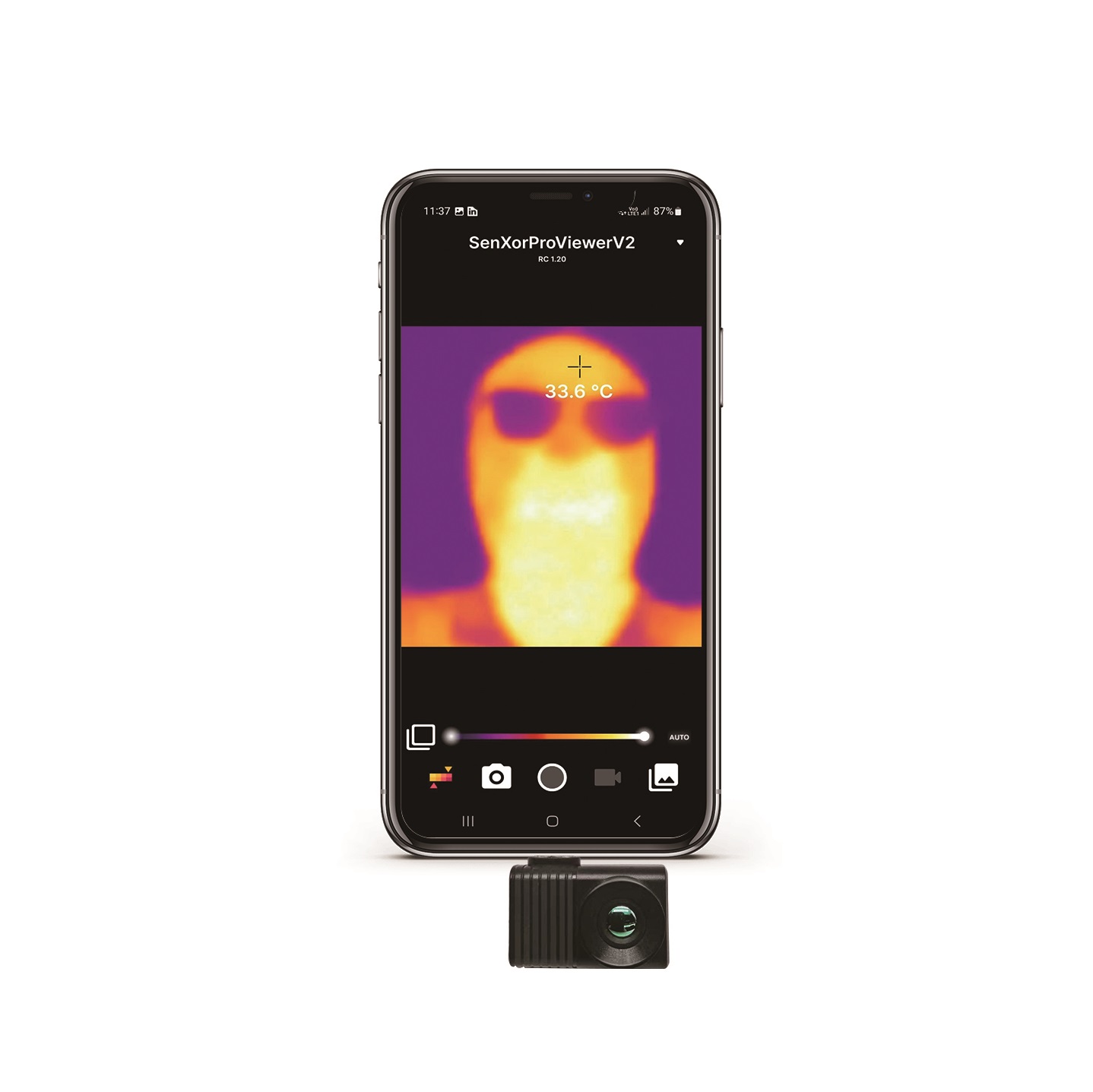
Qualitative thermal imaging prioritizes visual scene contrast for human inspection or basic optical tracking. Qualitative engines utilize aggressive Automatic Gain Control (AGC) algorithms—such as histogram equalization or plateau equalization—that stretch the sensor's 8-bit display dynamic range based purely on the hottest and coldest pixels in the current field of view. While helpful for piloting a drone past obstacles in total darkness, qualitative thermography discards the physical thermodynamic relationship between pixel counts and real-world target temperatures. If a hot object suddenly enters the field of view, the qualitative AGC recalibrates the entire scene, causing background objects to change brightness dynamically.
Quantitative radiometry transforms the compact thermal core into an absolute, non-contact thermodynamic measuring instrument. Rather than discarding raw values, the radiometric engine outputs an uncompressed 14-bit or 16-bit stream where every single pixel value represents a calibrated energy reading. The processing host solves the inverted Planck's Radiation Law in real time, incorporating critical thermodynamic compensation factors:
- ⚙️ Target Emissivity (ε): The measure of an object's efficiency in radiating infrared energy relative to a theoretical blackbody. Bare, polished aluminum traces on a circuit board may feature an emissivity as low as ε ≈ 0.04, causing them to reflect ambient room heat like a mirror and yield false readings unless mathematically corrected by the radiometric engine. Conversely, standard FR4 epoxy fiberglass boards and IC epoxy packages feature high emissivities (ε ≈ 0.90 to 0.95).
- ⚙️ Reflected Ambient Temperature (Trefl): Radiant energy originating from surrounding environmental heat sources bouncing off the target surface into the camera objective.
- ⚙️ Atmospheric Attenuation: Signal loss caused by atmospheric moisture, carbon dioxide absorption, and particulate scattering over operational distances exceeding 100 meters.
OEM systems utilizing Edge-AI—such as micro-inspection robots tracking automated production yields, or autonomous drones patrolling energy corridors—rely on these per-pixel radiometric arrays to run algorithmic safety triggers. For an in-depth breakdown of radiometric raw temperature calibration math, reference our comprehensive engineering guide on radiometric thermal camera module OEM integration.
6. OEM Benchmark: Mini 256 vs. Mini2 640 Product Comparison
To assist systems architects in specifying thermal hardware for next-generation platforms, this section benchmarks two field-proven, high-performance compact thermal imaging camera modules engineered for drone integration and micro-inspection assemblies.
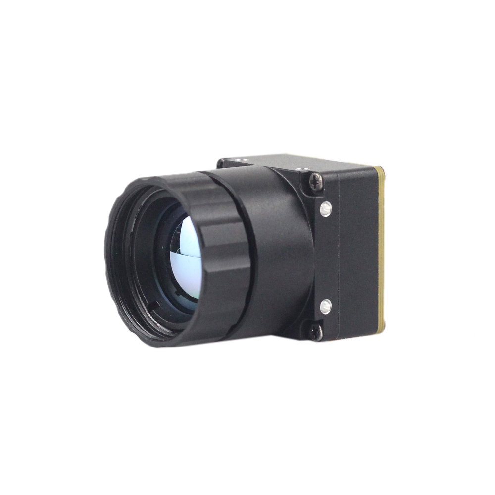
Mini 256 Uncooled LWIR Thermal Camera Module
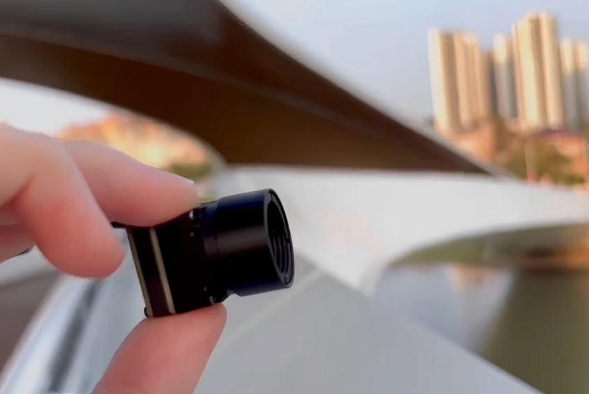
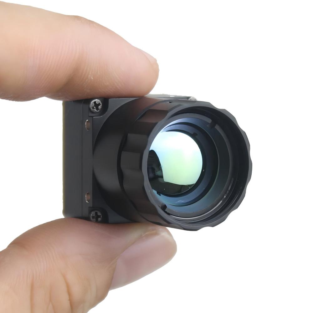
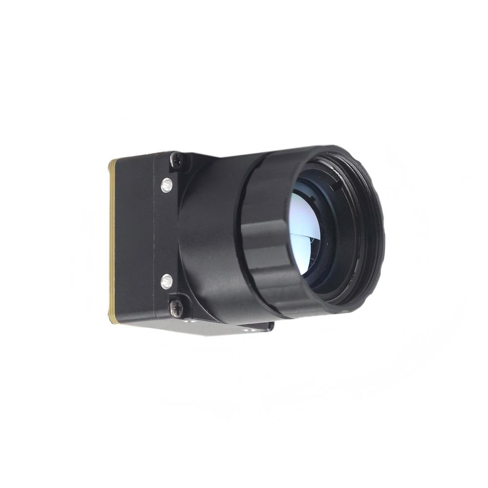
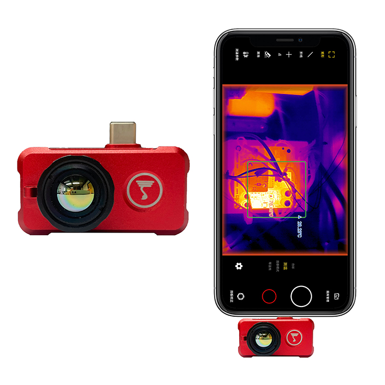
The Mini 256 Uncooled LWIR thermal Camera Module adopts high-performance infrared detectors for ultra-clear thermal imaging and accurate temperature measurement. Engineered as an ultra-compact, high-agility core, it captures infrared radiation and outputs a uniform thermal image with radiometry. With dimensions comparable to drone platforms similar to DJI for detecting mines, this module is built for ultra-low payload environments where every gram and milliwatt determines operational viability.
- ✅ Resolution: 256 × 192 pixels (12 µm VOx microbolometer)
- ✅ Thermal Sensitivity: ≤ 50 mK (@ f/1.0, 25°C)
- ✅ Physical Profile: Postage-stamp form factor for tight integration
- ✅ Output Mode: Industrial radiometry with full point, line, and area temperature capture
Mini2 640×512 9mm Thermal Imaging Camera Module For Drones
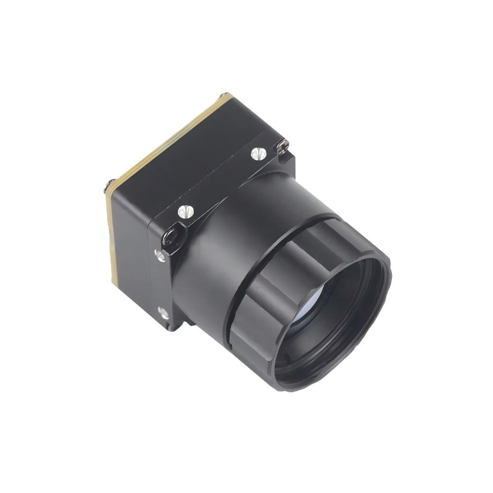
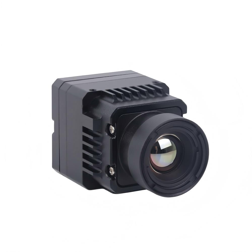
The Uncooled Infrared Mini2 640x512 9mm Thermal Imaging Camera Module For Drones features sharp and crisp image presentation, compact size, and low cost. Designed specifically for integration into small airborne platforms, inspection gimbals, and high-density industrial systems, this micro uncooled infrared thermal imaging module bridges the gap between high spatial clarity and constrained SWaP-C requirements.
- ✅ Resolution: 640 × 512 pixels (over 327,000 spatial measurement points)
- ✅ Lens System: High-precision 9mm athermalized optical assembly
- ✅ Thermal Sensitivity: ≤ 40 mK for resolving faint thermal boundaries
- ✅ Embedded Ready: Native MIPI CSI-2 interface for direct edge computing
Direct Engineering Specification Matrix
| System Parameter | Mini 256 LWIR Module | Mini2 640×512 9mm Drone Module |
|---|---|---|
| Detector Array Size | 256 × 192 (49,152 pixels) | 640 × 512 (327,680 pixels) |
| Pixel Pitch & Material | 12 µm, Uncooled Vanadium Oxide (VOx) | 12 µm, Uncooled Vanadium Oxide (VOx) |
| Spectral Response | 8 µm to 14 µm (LWIR) | 8 µm to 14 µm (LWIR) |
| Thermal Sensitivity (NETD) | ≤ 50 mK (@ f/1.0, 25°C) | ≤ 40 mK (@ f/1.0, 25°C) |
| Optical Configuration | Ultra-wide athermalized micro-lens | 9mm athermalized prime objective |
| Electrical Interface Options | USB / CMOS / Parallel (configurable) | Native MIPI CSI-2 / DVP / USB |
| Radiometric Precision | Supported (Point, Line, Area temp analytics) | Full-frame calibrated 14-bit radiometry |
| Approximate Bare Core Mass | ∼18g to 25g (bracket dependent) | ∼30g to 42g (including 9mm lens) |
| Application Target | Sub-250g Drones, Mine Detection, Rapid SMT Checks | Enterprise Inspection UAS, Micro-Trace PCB AOI, Edge AI |
For engineering teams evaluating sensor cores across higher resolution classes and alternate optical form factors, explore our detailed overview of high-resolution thermal imaging camera modules.
7. Application Blueprints: Sub-250g Drones vs. Micro-Inspection Benches
Executing a reliable thermal core integration requires careful attention to the operational mechanics of the parent host system. Airborne and benchtop inspection environments impose contrasting electrical and physical design requirements.
Blueprint A: Sub-250g Airborne Payload Architecture
In a sub-250g aerial platform, electrical noise, mass imbalances, and thermal variations interact simultaneously:
- ⚙️ Power Conditioning and Clean Regulation: Connecting a thermal core directly to unregulated battery buses introduces ripple that damages analog microbolometer readouts. Brushless drone motors draw dynamic current spikes, creating severe voltage drops and high-frequency switching noise across the battery lines. The compact thermal imaging camera must be powered by an isolated, high-efficiency synchronous buck regulator followed by an ultra-low-dropout (LDO) linear regulator to deliver clean, ripple-free DC power (< 15mV RMS noise).
- ⚙️ Micro-Gimbal Dynamic Mass Balancing: To prevent jitter in airborne thermal feeds, the center of gravity (CG) of the camera core, lens barrel, and flex-interconnect PCB must align precisely with the rotational pitch and roll axes of the micro-gimbal. Off-center loads force brushless gimbal motors to consume excess current to maintain stabilization, overheating the gimbal actuators and inducing mechanical oscillations.
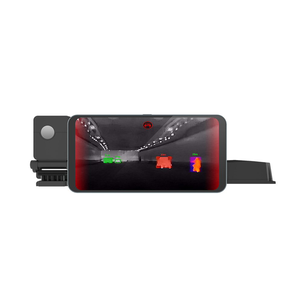
- ⚙️ Sub-Surface Mine and Explosive Remnant Detection: Buried metallic and non-metallic landmines alter the density, thermal conductivity, and moisture retention of surrounding soil. Over daily heating and cooling cycles, ground immediately above buried ordnance shifts temperature at a different rate than undisturbed earth. High-sensitivity compact cores (such as the Mini 256 or Mini2 640) can detect these subtle thermal boundaries from low-altitude flight paths, providing automated stand-off hazard mapping. Similar infrared spatial modeling techniques are used in advanced mobile platforms, as analyzed in our review of infrared thermal imaging autonomous navigation.
Blueprint B: Micro-Inspection Automated Test Equipment (ATE) Bench
Automated optical inspection and micro-electronics engineering benches deploy compact thermal imaging cores to diagnose sub-millimeter component issues:
- ⚙️ Isolating Hairline Power-Rail Shorts: When power planes short out due to manufacturing micro-whiskers, solder bridging, or dielectric breakdown beneath ball-grid arrays (BGAs), traditional multimeter continuity tests can confirm the existence of a short, but cannot locate its physical coordinates. By feeding a current-limited DC voltage into the shorted rail, electrical energy dissipates as heat at the point of greatest resistance. A compact 640×512 core positioned at a 100mm to 150mm working distance resolves the resulting micro-watt thermal signature, pinpointing the short within seconds.
- ⚙️ Die-Level Micro-Cracking and TIM Voids: Bare-die silicon components and Flip-Chip packaging experience thermal stress during dynamic load testing. Incomplete thermal interface material (TIM) coverage manifests as localized hot zones across the die face. The high spatial density of modern 12 µm cores reveals these thermal gradients, allowing automated vision algorithms to reject defective boards before final product assembly.
8. Thermal Drift, In-Flight Calibration, and Environmental Hardening
Because microbolometers measure microscopic changes in internal membrane resistance, any temperature fluctuation across the camera housing, lens barrel, or chassis alters sensor readings. Engineering a reliable system requires proactive thermal stabilization and shielding.
Mechanical Shutter Calibration vs. Shutterless SBNUC Engines
As ambient temperatures drift, individual microbolometer pixels experience variable drift, causing fixed-pattern noise (FPN) that degrades image quality over time:
- ⚙️ Mechanical Shutter Assemblies: Traditional camera cores address this drift using a motorized mechanical shutter paddle. At scheduled intervals or upon detecting internal temperature shifts, a miniature solenoid swings a uniform-temperature paddle into the optical path for 150ms to 350ms. The camera takes a flat-field reference image and recalibrates its pixel offset tables. While reliable, this mechanical cycle temporarily freezes video output and introduces moving components vulnerable to wear in high-vibration drone environments.
- ✅ Shutterless Algorithmic NUC (SBNUC): Advanced modern cores combine internal thermistor networks with Scene-Based Non-Uniformity Correction algorithms. Embedded thermistors track thermal gradients across the lens assembly and sensor chassis in real time, while mathematical motion algorithms continuously filter out stationary pixel-to-pixel fixed-pattern noise without requiring a mechanical shutter paddle. This eliminates mechanical failure points and ensures uninterrupted video feeds—a critical requirement for flight-critical aerial navigation and automated production lines.
Electromagnetic Hardening Near Brushless Motors and Radio Transmitters
A compact thermal imaging camera core integrated into an airborne platform frequently operates within centimeters of powerful electromagnetic interference (EMI) sources, including 5.8GHz video transmitters, telemetry antennas, electronic speed controllers (ESCs), and high-frequency motor phase wiring. Unshielded microbolometer circuits readily pick up this RF noise, which manifests as horizontal banding, ghost lines, or corrupted radiometric metadata.
To protect signal integrity, follow these essential EMI mitigation practices:
- ⚙️ Enclose the thermal sensor core within an electrically continuous Faraday shield, utilizing thin copper foil tape or nickel-plated structural enclosures tied directly to the central chassis ground.
- ⚙️ Route high-speed MIPI CSI-2 differential pairs with matched 100-ohm differential impedance ($\pm 10\%$) across internal ground-plane-shielded flex layers, avoiding parallel routing alongside motor phase wires.
- ⚙️ Place broad-spectrum ferrite suppression beads and ceramic decoupling capacitors directly adjacent to the camera core's primary DC input connector to filter out high-frequency transient spikes.
9. Frequently Asked Questions (FAQ)
Can a compact thermal imaging camera fit within sub-250g drone platforms?
Is a 256x192 compact thermal camera sufficient for PCB inspection, or is 640x512 necessary?
What is the practical difference between consumer thermal gadgets and industrial radiometric cores?
📚 References & Further Reading
- Industry Standard: High-speed processing platforms and single-board embedded systems: Raspberry Pi Foundation
- Industry Standard: Micro-miniature high-density flex-circuit board-to-board interconnects: Molex Interconnect Solutions
- Related Guide: Embedded radiometric sensor architecture and raw data calibration: Radiometric Thermal Camera Module OEM Integration
- Related Guide: High-resolution microbolometer module selection for enterprise payloads: Top Thermal Infrared Camera Cores & Modules
- Related Guide: Long-wave infrared sensor deployment in autonomous guidance and vehicle perception: Infrared Thermal Imaging in Autonomous Driving