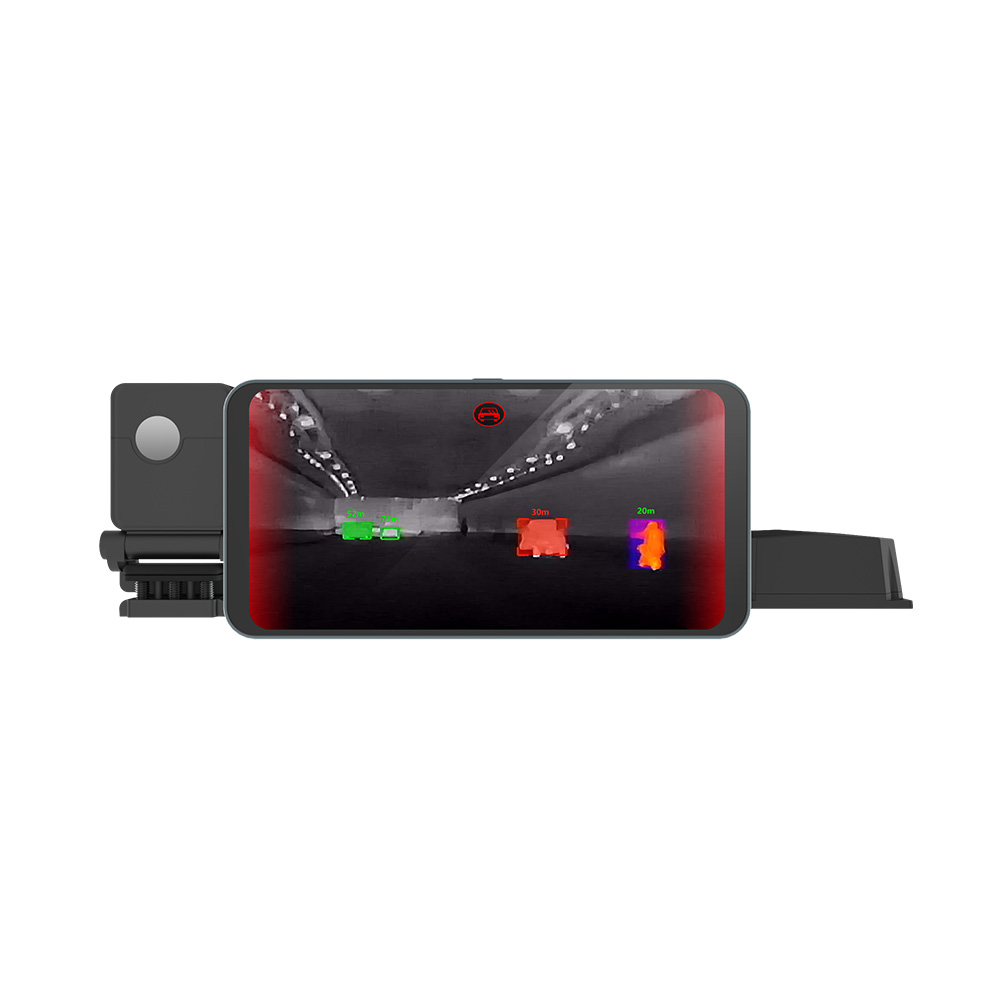

Cheap Thermal Imaging Camera Guide: Stop Buying Blurry Gimmicks (Real 256+ Cores)
2026年10月30日
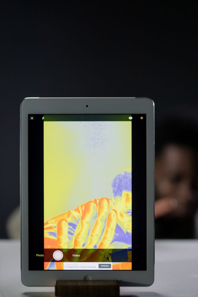
How Does a Thermographic Camera Work? The Complete Tech & Hardware Guide
At the macroscopic physical level, every object with a temperature above absolute zero (0 Kelvin or -273.15°C) emits electromagnetic radiation governed by Planck’s radiation law and the Stefan-Boltzmann relationship. Unlike standard electro-optical (EO) sensors that rely on reflected ambient visible light (380 to 750 nm) focused onto silicon CMOS or CCD matrices, a thermographic camera operates in the invisible infrared spectrum—specifically targeting the Long-Wave Infrared (LWIR) atmospheric transmission band between 8 and 14 μm. Rather than rendering visible surfaces, a thermographic system maps self-emitted thermal radiant flux, translating microscopic variations in infrared flux density into high-contrast digital representations known as thermograms.
For optical engineers, drone payload architects, and industrial automation integrators, deploying thermal imaging requires looking past external enclosures into the core optoelectronic pipeline. This begins with specialized chalcogenide or monocrystalline germanium optics, transfers through a vacuum-packaged microbolometer Focal Plane Array (FPA), converts across a Read-Out Integrated Circuit (ROIC), and finishes inside an Image Signal Processor (ISP) executing non-uniformity correction and radiometric algorithms. Understanding the hardware mechanics and physics behind thermal detectors is critical to designing reliable systems for automated condition monitoring, aerial search and rescue, defense, and machine vision.
جدول المحتويات
- 👉 1. The Fundamental Physics of Thermography: Emission, Emissivity, and the LWIR Window
- 👉 2. Optoelectronic Anatomy: Step-by-Step Hardware Signal Flow
- 👉 3. Microbolometer Sensor Architecture: VOx, Pixel Pitch, and NETD Mechanics
- 👉 4. Thermal Optics Engineering: Germanium, Chalcogenide, and f-Number Performance
- 👉 5. Sensor Interfacing, Signal Transmission, and Hardware Protocols
- 👉 6. OEM Thermal Imaging Hardware: Industrial Product Specifications & Benchmarks
- 👉 7. Radiometric Calibration: Non-Uniformity Correction (NUC), Shutter Flags, and Temperature Math
- 👉 الأسئلة الشائعة (FAQ)
1. The Fundamental Physics of Thermography: Emission, Emissivity, and the LWIR Window
To understand how a thermographic camera extracts quantitative temperature data from an observed scene, one must evaluate the physical principles formalized by Max Planck, Wilhelm Wien, and Josef Stefan. Any physical body comprised of vibrating atomic lattices emits electromagnetic waves. The total emissive power of a blackbody—a theoretical surface that absorbs all incident radiation and radiates at the thermodynamic limit—is expressed by the Stefan-Boltzmann law:
W = σ · T⁴
Where W represents radiant emittance expressed in Watts per square meter (W/m²), σ denotes the Stefan-Boltzmann constant (5.670374 × 10⁻⁸ W·m⁻²·K⁻⁴), and T signifies absolute thermodynamic temperature expressed in Kelvin (K). Because real-world materials are not ideal blackbodies, thermographic cameras must account for emissivity (ε), a dimensionless coefficient situated between 0.0 (a theoretical non-emitting, perfect reflector) and 1.0 (an idealized blackbody emitter). Radiant exitance from real materials is thus governed by:
W_real = ε · σ · T⁴
Conservation of energy dictates that when ambient thermal radiant energy encounters an arbitrary target surface, the total incident radiant flux must divide across three primary phenomenological pathways: emissivity (ε), reflectivity (ρ), and transmissivity (τ). These components satisfy the fundamental relationship ε + ρ + τ = 1.0. For the vast majority of solid industrial materials, opaque substrates, and dense targets, transmissivity is functionally zero (τ ≈ 0). Consequently, the radiometric camera sensor simultaneously captures both the direct self-emitted thermal energy from the target (governed by ε) and the indirect ambient radiation originating from surrounding environmental sources that bounces off the object's surface (governed by ρ = 1 - ε).
فيديو مباشر للتصوير الحراري
As documented in comprehensive physical overviews such as ويكيبيديا التصوير الحراري, Wien’s Displacement Law establishes that the peak spectral emission wavelength (λ_max) of any radiating blackbody shifts inversely with absolute temperature according to λ_max = b / T, where b represents Wien’s displacement constant (~2898 μm·K). For terrestrial targets, electrical machinery, and living organisms existing within standard ambient environmental windows (~300 Kelvin), the peak spectral exitance is concentrated within the 8 to 14 μm spectral domain.
This optical reality directly explains why uncooled industrial thermal imagers focus almost exclusively on the Long-Wave Infrared (LWIR) band spanning 8 to 14 μm. Within this specific spectral window, molecular absorption caused by atmospheric constituents—primarily gaseous water vapor (H₂O) and carbon dioxide (CO₂)—falls to localized minima. This clear atmospheric transmission corridor permits infrared photons to propagate across substantial geometric distances with minimal signal degradation, enabling clear, highly accurate thermal measurements through dense fog, atmospheric haze, particulate dust, and complete darkness. For specialized integration perspectives regarding night surveillance capabilities, engineers can review our regional technical breakdown on كاميرا تصوير حراري: عيون نارية في الليل (Thermal Imaging Cameras: Night Vision Mechanics).
Accounting for target emissivity requires evaluating surface morphology, oxidation states, and viewing angles. Polished bare metals, such as machined aluminum or rolled copper busbars, exhibit low emissivity values often between 0.04 and 0.15, meaning over 85% of the collected photon flux consists of ambient reflections rather than true thermal emission. Non-metallic industrial surfaces—such as electrical tape, matte polymer jackets, organic materials, and paint layers—present high emissivity values typically ranging from 0.90 to 0.97. In practical integration, uncorrected emissivity values lead to catastrophic radiometric offsets; miscalculating emissivity by 0.10 on a warm transformer terminal can skew calculated temperature readings by tens of degrees Celsius.
2. Optoelectronic Anatomy: Step-by-Step Hardware Signal Flow
A modern industrial thermographic camera module is a multi-tier optoelectronic assembly. It transforms photon flux from long-wave electromagnetic fields into calibrated radiometric values using a precisely timed hardware pipeline. Understanding each discrete stage of this pipeline allows systems designers to optimize image quality, minimize measurement latency, and preserve data integrity across mission-critical inspection frameworks.
The signal sequence proceeds through distinct hardware transitions:
- ⚙️ Optical Collection & Transmission: Incoming long-wave infrared radiant energy passes through an anti-reflective coated optical element, typically composed of monocrystalline Germanium or high-purity Chalcogenide glass. Because conventional optical glasses exhibit extreme absorption coefficients within the LWIR band, these specialized crystalline materials focus thermal radiation onto the sensor focal plane without substantial transmission loss.
- ⚙️ Mechanical Calibration Referencing: Immediately behind the rear optical element lies an electromechanically actuated shutter mechanism. Actuated by a miniature solenoid, this shutter briefly interposes a thermally uniform reference surface into the optical path to facilitate baseline sensor offset calibration.
- ⚙️ Photothermal Conversion at the FPA: Once focused by the optics, the thermal photons impinge upon a vacuum-encapsulated Focal Plane Array (FPA) consisting of thousands of microscopic, thermally isolated detection elements known as microbolometers. Each microbolometer absorbs incoming infrared photons, causing the temperature of its microscopic semiconductor membrane to rise or fall in proportion to scene radiance.
- ⚙️ Thermo-Resistive Transduction: This subtle temperature fluctuation induces a measurable change in the electrical resistance of the detector material, a physical phenomenon governed by the material's Temperature Coefficient of Resistance (TCR).
- ⚙️ ROIC Signal Integration & Multiplexing: Directly beneath the suspended micro-machined array, a custom silicon Read-Out Integrated Circuit (ROIC) applies pulsed bias voltages across each detector row and column. The minute resistance shifts of the individual bolometer pixels modulate the resulting electrical current, which is integrated across low-noise Capacitive Transimpedance Amplifiers (CTIAs) integrated directly into the ROIC substrate.
- ⚙️ التحويل من التناظري إلى الرقمي: The multiplexed analog voltage levels are routed to ultra-low-noise 14-bit or 16-bit Analog-to-Digital Converters (ADCs), which digitize the analog charges into raw, high-depth spatial digital matrices representing minute flux variations across the scene.
- ⚙️ Digital Processing & Radiometric Correction: The raw digital data is ingested by a dedicated Digital Signal Processor (DSP) or Field-Programmable Gate Array (FPGA). This processing engine executes complex, real-time corrections, including Non-Uniformity Correction (NUC), Bad Pixel Replacement (BPR), and temporal noise filtering. Next, a specialized radiometric engine calculates absolute temperatures for every pixel by inverting the Planck radiation equation, referencing factory-calibrated lookup tables, and factoring in user-supplied parameters such as target emissivity, ambient atmospheric temperature, relative humidity, and target distance.
- ⚙️ Output Encoding & Physical Streaming: The processed radiometric matrix is encoded for external transmission—either outputting raw digital temperatures over buses like MIPI CSI-2 or USB, or converting the data into false-color video streams (such as Ironbow or White-Hot) for transmission over analog CVBS or standard UVC display interfaces.
3. Microbolometer Sensor Architecture: VOx, Pixel Pitch, and NETD Mechanics
The core component of any modern uncooled thermographic camera is the microbolometer Focal Plane Array. Unlike cryogenic quantum infrared detectors (such as Indium Antimonide or Mercury Cadmium Telluride sensors that require bulky, power-hungry closed-cycle Stirling coolers operating down at 77 Kelvin), uncooled microbolometers operate reliably at standard ambient environmental temperatures ranging from -40°C to +85°C. This eliminates the size, weight, power, and maintenance overhead associated with mechanical cryogenic pumps.
A microbolometer pixel is a Micro-Electro-Mechanical Systems (MEMS) structure. It features an ultra-thin absorbing membrane suspended above a reflective silicon substrate by two long, highly engineered micro-machined anchor legs. These support legs serve two critical functions: they establish an electrical interconnect between the absorbing membrane and the underlying ROIC, and they provide extreme thermal isolation. By physically suspending the pixel membrane within a hermetically sealed vacuum cavity, thermal energy absorbed by the membrane cannot escape via physical conduction or atmospheric convection. It can only dissipate through the narrow support legs, maximizing thermal sensitivity.
The thermal time constant (τ_th) of each microbolometer pixel dictates how fast the sensor responds to dynamic thermal transitions. This is expressed mechanically by the ratio of heat capacity to thermal conductance:
τ_th = C_th / G_th
Where C_th represents the heat capacity of the suspended membrane (Joules per Kelvin) and G_th represents the thermal conductance of the anchor legs (Watts per Kelvin). Designing a competitive pixel requires minimizing G_th to trap heat and boost temperature rise, while simultaneously reducing C_th to prevent the thermal time constant from ballooning past the sensor frame period (typically 20ms to 40ms for 50Hz/25Hz video). If C_th is too high, thermal memory persists across consecutive frames, generating smearing artifacts during high-speed motion.
The active sensing thin-film layer of the membrane is primarily manufactured from one of two functional materials: Vanadium Oxide (VOx) or Amorphous Silicon (a-Si). Vanadium Oxide is the superior semiconductor material for high-performance industrial and military systems. VOx possesses a high negative Temperature Coefficient of Resistance (TCR typically ranging from -2%/K to -3%/K at room temperature) combined with exceptionally low 1/f flicker noise characteristics. Amorphous Silicon, while compatible with standard commercial CMOS fabrication infrastructure and offering lower manufacturing costs, suffers from significantly higher structural internal stress and elevated intrinsic electrical noise. As a result, a-Si arrays often exhibit higher noise floors and slower response times when scaled down to smaller pixel architectures.
Over recent years, the thermal imaging industry has transitioned from larger 35μm, 25μm, and 17μm manufacturing processes to the modern 12μm pixel pitch node. Decreasing the pixel pitch to 12μm yields profound engineering advantages:
- ✅ Die Footprint Reduction: The total physical surface area of the Focal Plane Array is reduced by more than 50% for an equivalent pixel resolution (such as 384×288 or 640×512), dramatically lowering silicon die fabrication costs.
- ✅ التصغير البصري: Shorter focal length lenses deliver identical target Fields of View (FOV), substantially shrinking Germanium optic diameters and mechanical barrel lengths.
- ✅ SWaP Envelope Optimization: The resulting reduction in optical glass diameter dramatically lowers payload weight and mechanical volume—critical factors for stabilizing high-speed drone gimbals and autonomous mobile robots.
- ✅ Faster Pixel Dynamics: The smaller physical mass of a 12μm pixel membrane yields a lower thermal capacitance, enabling faster pixel response time constants (often dropping below 10 milliseconds) to eliminate motion blur during rapid panning.
The definitive figure of merit evaluating thermal detector sensitivity is Noise Equivalent Temperature Difference (NETD), expressed in millikelvins (mK). NETD quantifies the minimum target temperature differential that produces a signal-to-noise ratio of unity (SNR = 1) at the sensor output. Lower numerical NETD values indicate superior sensitivity. Modern industrial-grade microbolometer cores consistently deliver NETD ratings of ≤40mK (measured at f/1.0 aperture and 25°C ambient). A sensor rated at 40mK can clearly distinguish temperature differences as slight as 0.04°C, allowing it to expose minor thermal signatures such as subsurface composite delaminations, resistive micro-faults inside electrical enclosures, and early-stage building envelope insulation gaps.
4. Thermal Optics Engineering: Germanium, Chalcogenide, and f-Number Performance
Optical design for thermographic systems operating within the 8 to 14 μm LWIR band presents unique challenges compared to visible-spectrum lens design. Conventional borosilicate glasses (such as standard N-BK7) absorb LWIR radiation within their first few micrometers of thickness. As a consequence, optical engineers must utilize specialized infrared-transmitting optical substrates that exhibit high transmissivity, mechanical stability, and predictable dispersion profiles across the LWIR spectrum.
Monocrystalline Germanium (Ge) remains the premier substrate for high-resolution LWIR optics. Germanium provides an exceptionally high refractive index (n ≈ 4.00 at 10.0 μm), allowing optical engineers to achieve substantial optical power and wide apertures using lenses with relatively flat surface curvatures. This minimizes spherical aberrations without requiring complex multi-element lens designs. However, Germanium has a significant drawback: an exceptionally high thermo-optic coefficient (dn/dT ≈ 3.96 × 10⁻⁴ /°C), meaning its refractive index shifts noticeably with changes in ambient temperature. Left unaddressed, a Germanium lens will rapidly defocus as operational temperatures fluctuate. Optical assemblies must therefore incorporate mechanical or optical athermalization techniques, pairing Germanium with compensating materials or mechanical sleeves. Additionally, polished Germanium exhibits high surface reflectivity (Fresnel losses exceeding 36% per untreated optical surface), requiring high-durability Anti-Reflective (AR) coatings and Diamond-Like Carbon (DLC) exterior coatings to survive abrasive field conditions.
Chalcogenide glasses (such as GASIR, Ge-Sb-Se glass matrix formulations) provide an appealing alternative to Germanium. While their refractive index is lower (n ≈ 2.5 to 2.8), Chalcogenide materials can be hot-molded into precision aspheric and diffractive elements, bypassing the costly, time-consuming diamond-turning processes required for Germanium. Furthermore, Chalcogenide glasses feature a substantially lower thermo-optic coefficient, simplifying passive optical athermalization across wide operating ranges (-40°C to +85°C). In many high-performance optical designs, engineers pair Germanium and Chalcogenide elements within a doublet configuration to simultaneously correct chromatic aberrations and thermal drift.
Another fundamental parameter in thermal optical design is the optical aperture ratio, or f-number (f/#), defined as the ratio of the lens focal length to the entrance pupil diameter. The radiant flux (E) reaching the microbolometer surface is inversely proportional to the square of the lens f-number:
E ∝ 1 / (f/#)²
A thermal lens operating at f/1.0 transmits four times more radiant thermal flux than an f/2.0 lens of identical focal length. Designing an uncooled LWIR system with a high f-number (e.g., f/1.4 or f/1.6) severely reduces the signal reaching the sensor, artificially degrading the system's effective NETD and obscuring low-contrast thermal targets. As a result, industrial thermal systems are built around low f-number optics (typically f/1.0 to f/1.2) to maintain maximum thermal sensitivity.
5. Sensor Interfacing, Signal Transmission, and Hardware Protocols
Integrating a bare thermal camera core into an industrial machine vision cell, drone payload, or robotic monitoring platform requires careful selection of the physical and electrical interfaces. These buses directly determine latency, transmission bandwidth, processing overhead, and physical connector longevity in harsh environments.
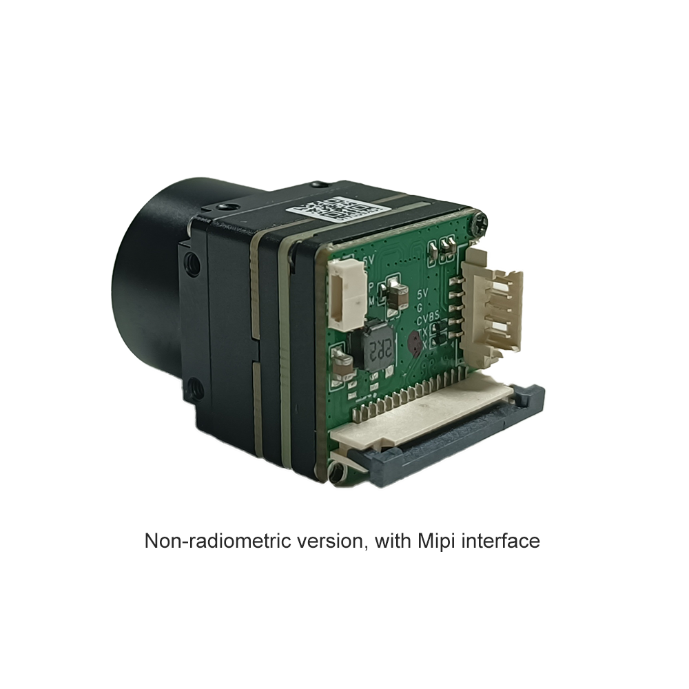
- ⚙️ MIPI CSI-2 Embedded Protocol: For edge computing platforms utilizing modern high-density System-on-Chips (SoCs)—such as the NVIDIA Jetson Orin, NXP i.MX8, or Rockchip platforms—the MIPI CSI-2 interface provides the highest performance. MIPI CSI-2 is a unidirectional, high-speed differential protocol that routes raw pixel data directly into the host processor's Image Signal Processing block via Direct Memory Access (DMA). By bypassing USB host controller stacks, it delivers sub-millisecond frame delivery times for uncompressed 14-bit or 16-bit radiometric telemetry frames, critical for autonomous obstacle avoidance and high-speed robotic sorting.
- ⚙️ USB Video Class (UVC) & CDC Serial: For industrial PCs and benchtop testing equipment, USB 2.0/3.0 interfaces configured via standard UVC drivers provide cross-platform plug-and-play capability. Modules split data into dual endpoints: an 8-bit YUV/RGB stream for direct visual inspection and a secondary CDC virtual COM port or vendor endpoint carrying 14-bit radiometric per-pixel matrices for external temperature quantification.
- ⚙️ Low-Latency Analog CVBS: Standard Composite Video Blanking and Sync (CVBS) in NTSC or PAL formats is driven by integrated video DACs on the thermal module. Bypassing packet encapsulation and memory buffering, CVBS enables instantaneous analog transmission over 5.8 GHz video transmitters for FPV drone pilots and defense gimbal operators who cannot tolerate the 60–120ms latencies inherent in digital video encoding.
- ⚙️ Industrial GigE Vision & GenICam: In plant automation, thermal sensors communicate over Gigabit Ethernet networks using GigE Vision protocols. This facilitates long cable runs (up to 100 meters over standard Cat6 copper) with deterministic frame delivery, hardware trigger synchronization, and unified camera configuration through GenICam XML registers.
To withstand mechanical vibration and continuous shock in dynamic applications, embedded thermal cores rely on rugged board-to-board (B2B) connectors. Industry-standard fine-pitch connectors, such as the ultra-compact DF40 series from هيروس إلكتريك, provide secure, high-density connections with multi-point contact systems. These miniature connectors maintain absolute signal integrity across high-speed differential pairs, power rails, and control buses like I2C, SPI, and UART, ensuring reliable operation in high-g drone maneuvers and industrial automation cells.
For additional details on interface design and physical integration, refer to our comprehensive engineering guides on الدليل الشامل لدمج كاميرا الوحدة الحرارية (Comprehensive Thermal Camera Module Integration Guide) و Полное руководство по интеграции тепловизионных модулей (Full Integration Guide for Thermal Modules).
6. OEM Thermal Imaging Hardware: Industrial Product Specifications & Benchmarks
Selecting the right thermal imaging hardware requires evaluating physical parameters, electrical interfaces, and detector technologies against specific operational envelopes. Below are two industry-standard thermal camera modules engineered for high reliability, precision temperature measurement, and flexible system integration:
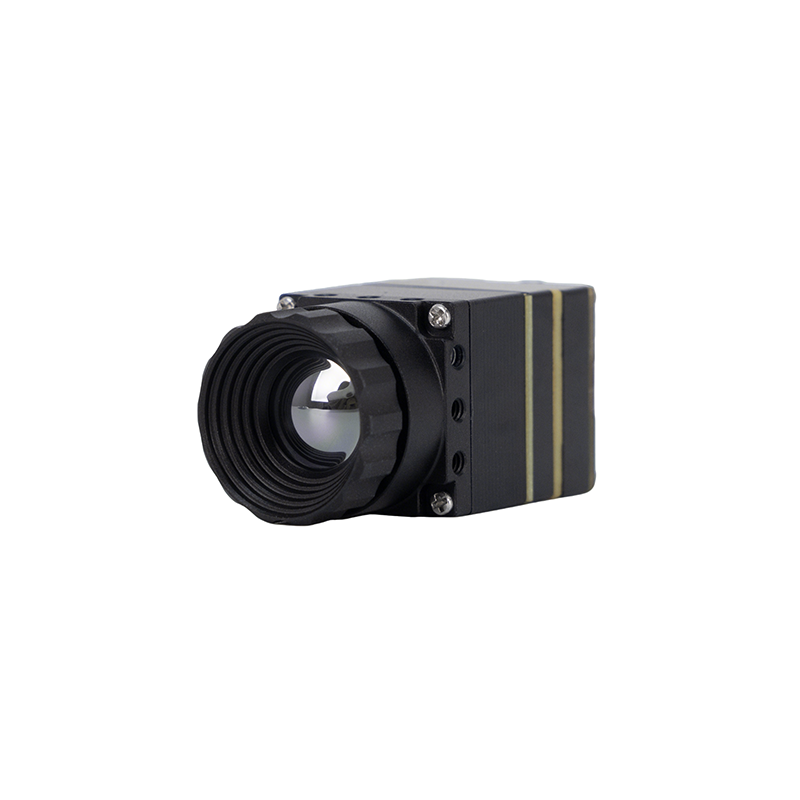
وحدة الكاميرا الحرارية غير المبردة MD Series بدقة 384x288 بالأشعة تحت الحمراء
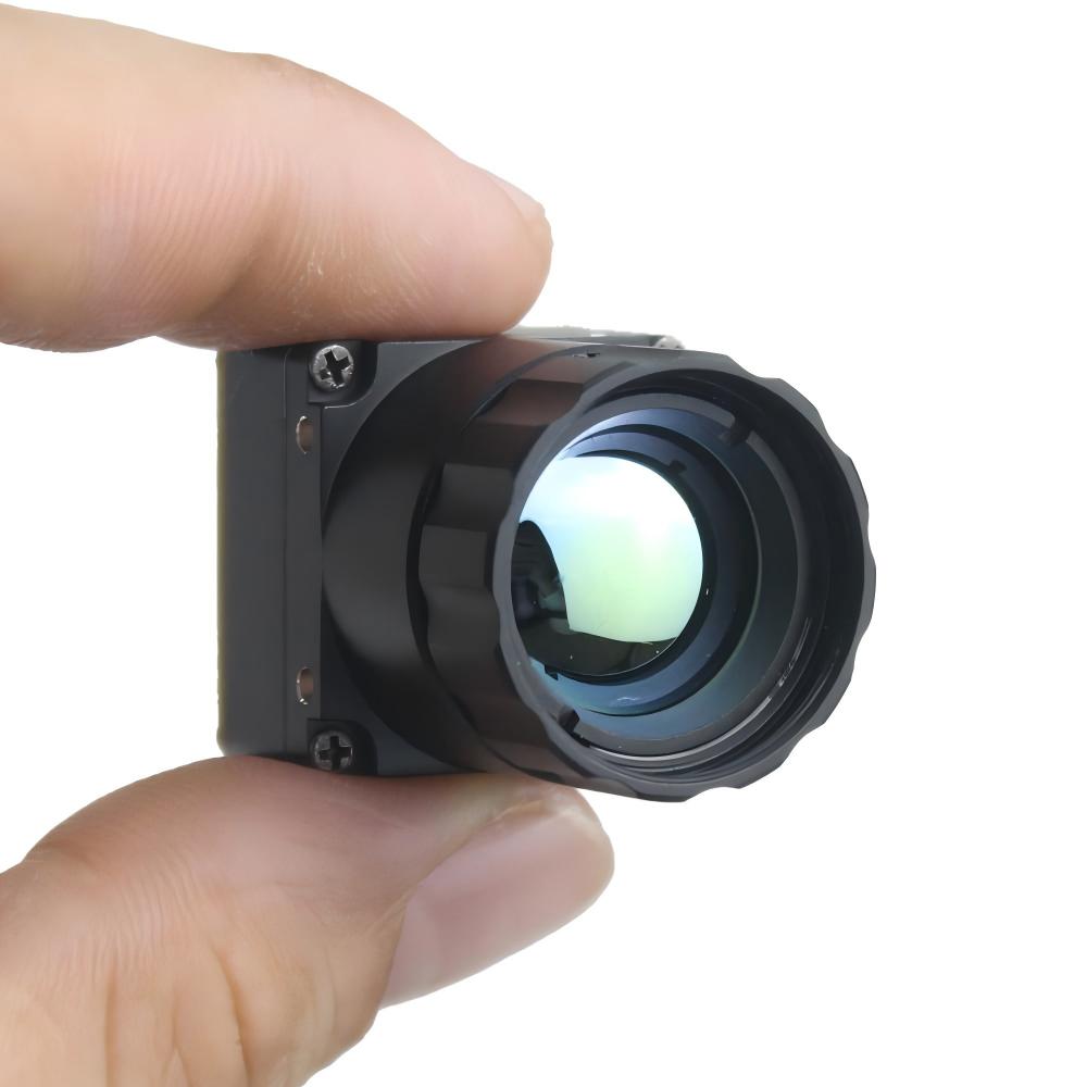
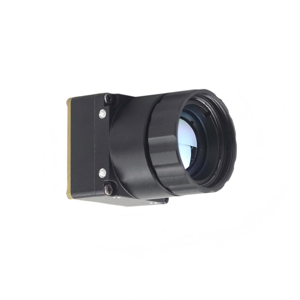
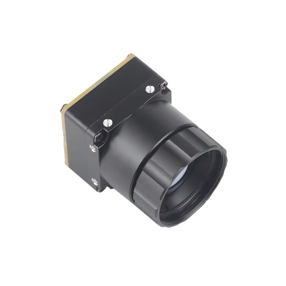
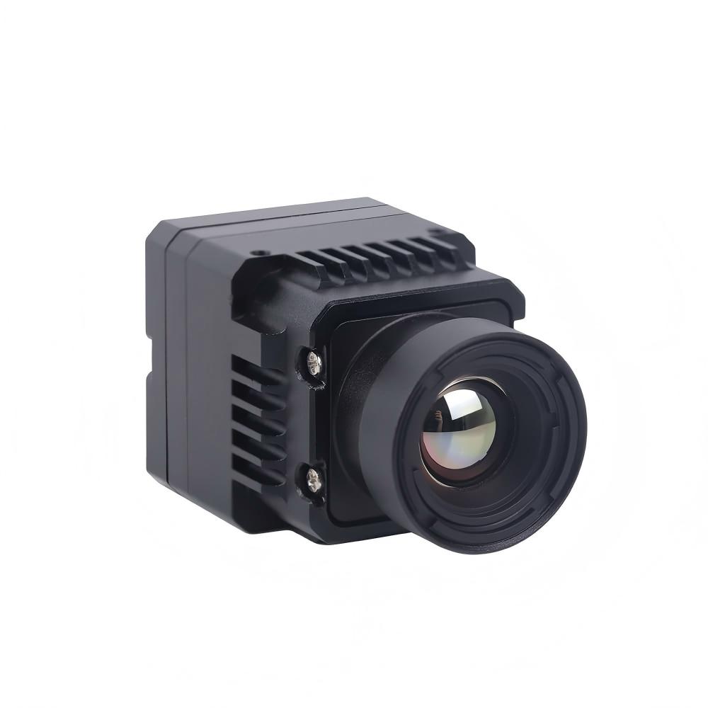
The Purpleriver MD Series thermal camera module is designed for industrial-grade precision in demanding applications including continuous perimeter security, online temperature monitoring, robotics, and aerial drone payloads. At its core, the module features an uncooled infrared focal plane array built on an advanced 12μm pixel pitch node, delivering exceptional thermal sensitivity, low noise, and sharp spatial imagery. Its compact dimensions, true plug-and-play architecture, and native support for multiple hardware interfaces—including MIPI CSI-2, USB 2.0, and analog CVBS—enable straightforward integration across embedded Linux architectures and standard vision controllers. Developed by an engineering team drawing from the Hong Kong University of Science and Technology and former Huawei HiSilicon semiconductor groups, the MD Series offers extensive OEM/ODM customization options across optical configurations, communication protocols, and custom firmware algorithms.
| معمارية الكاشف | مقياس ميكروبولومتر VOx غير مبرد بالأشعة تحت الحمراء |
| Spatial Pixel Resolution | 384 × 288 بكسل |
| Pixel Pitch Node | 12 ميكرومتر |
| Spectral Transmission Window | 8 – 14 μm (Long-Wave Infrared) |
| الواجهات المدعومة | MIPI CSI-2 / USB 2.0 / CVBS Analog |
| Integration Capabilities | Plug-and-play, full OEM/ODM firmware & optical options |
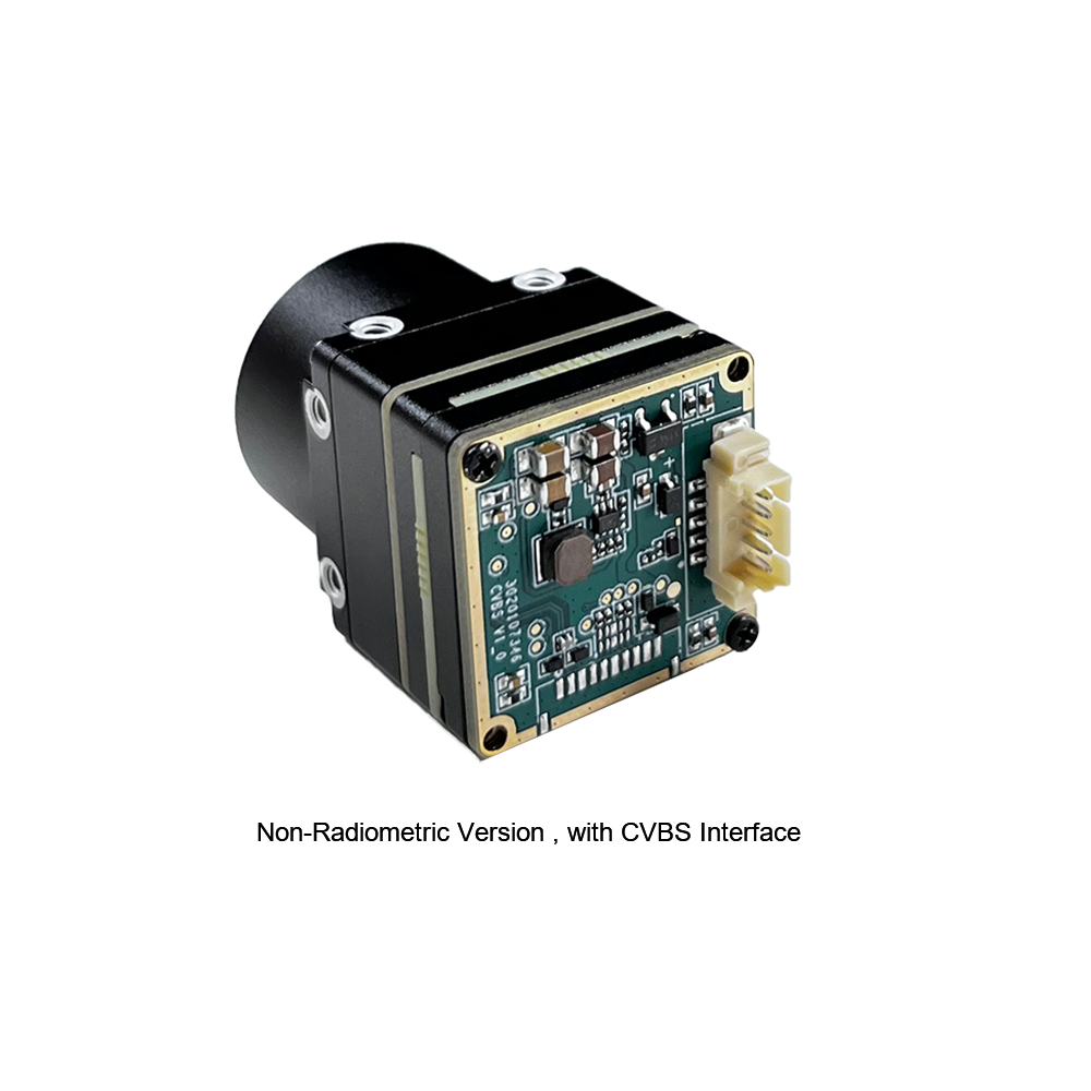
Uncooled MINI 384x288 Thermal Camera Module For Drones
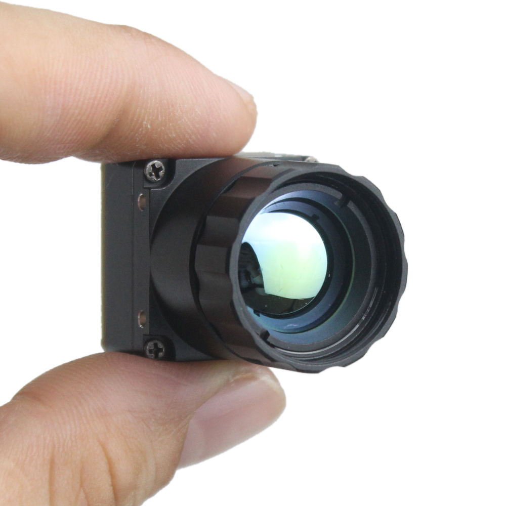
The MINI series infrared thermal imaging module is an ultra-compact, high-precision thermal imaging core designed specifically for weight-constrained aerial systems and online temperature measurement. Utilizing advanced uncooled detector designs and high-resolution imaging circuitry, the MINI core delivers reliable, stable performance across demanding operational environments. It supports multiple interface standards, making it an ideal choice for robotic drone payloads, machine vision inspection, perimeter safety, automated industrial manufacturing, and critical equipment maintenance. Its lightweight, low-power design ensures minimal impact on aerial flight times and gimbal stabilization systems.
| Primary Design Focus | SWaP-optimized for drone gimbals & mobile robotics |
| Spatial Pixel Resolution | 384 × 288 بكسل |
| Measurement Mechanics | Universal high-precision online radiometric measurement |
| عرض النطاق الطيفي | 8 – 14 μm (LWIR) |
| Output Video Connectivity | Multi-interface configuration (CVBS Analog / Digital Data) |
| Target Industrial Sectors | UAV airborne inspection, robotics, plant equipment maintenance |
7. Radiometric Calibration: Non-Uniformity Correction (NUC), Shutter Flags, and Temperature Math
A bare microbolometer array cannot produce a reliable thermal image or quantitative temperature data without active run-time compensation. Due to microscopic manufacturing tolerances inherent in MEMS lithography, each individual pixel on a Focal Plane Array exhibits subtle variations in active resistance, thermal capacitance, and Temperature Coefficient of Resistance. Left uncorrected, these pixel-to-pixel variations create Fixed-Pattern Noise (FPN)—a static mesh of vertical streaks and spatial grain that obscures the thermal scene. Transforming raw sensor voltages into accurate radiometric values requires a multi-stage calibration pipeline.
The initial stage is Non-Uniformity Correction (NUC). During factory calibration, the camera module is exposed to precision cavity blackbody sources set to uniform temperatures across low and high calibration points. The system evaluates the unique response of each detector pixel, calculating specific gain coefficients (G_i,j) and baseline offset values (O_i,j) to equalize the array's response:
V_corrected(i,j) = G_i,j · V_raw(i,j) + O_i,j
These calibration coefficients are stored in non-volatile EEPROM on the module. However, during active operation, thermal gradients develop across the camera housing and lens barrel as internal electronics warm up and ambient temperatures fluctuate. This thermal drift causes the offset coefficients of the individual pixels to diverge over time. To restore image uniformity, the module performs periodic Flat-Field Correction (FFC).
The operational mechanics of Flat-Field Correction involve sequential algorithmic actions:
- ⚙️ Solenoid Deployment: A micro-solenoid inserts a high-emissivity mechanical blade (the shutter flag) into the optical path between the rear optical element and the focal plane array for 100 to 250 milliseconds.
- ⚙️ Uniform Exposure Capture: With the shutter presenting an isothermal scene to the entire array, the ISP captures one or more reference frames.
- ⚙️ Offset Recalculation: Individual pixel drift is calculated against the array-wide average, generating an updated offset compensation matrix (O_i,j) that subtracts newly accumulated drift.
- ⚙️ Shutter Retraction & Normal Streaming: The flag retracts, restoring optical exposure with completely refreshed spatial uniformity and zero residual fixed-pattern noise.
In high-end aerospace and military gimbals where mechanical shutters may introduce reliability concerns or briefly interrupt the video feed, engineers deploy shutter-less algorithms. These software pipelines use temperature thermistors placed along the lens barrel and sensor housing to mathematically model thermal gradients, updating pixel offsets dynamically in software via Scene-Based Non-Uniformity Correction (SBNUC).
Once Non-Uniformity Correction is applied, the radiometric calculation engine converts the linearized digital counts into absolute temperature values. The total radiant flux collected by the sensor (S_total) combines energy from three distinct sources:
S_total = ε · τ_atm · S_obj + (1 - ε) · τ_atm · S_refl + (1 - τ_atm) · S_atm
The primary component is the target's direct thermal emission, scaled by surface emissivity (ε) and atmospheric transmission (τ_atm). The second component represents ambient background radiation (S_refl) reflecting off the target surface (scaled by reflectivity, ρ = 1 - ε) and transmitted through the atmosphere. The final component is the thermal radiation emitted by the atmospheric path itself (S_atm) between the object and the lens. The camera's processing engine isolates the object signal (S_obj) using calibrated parameters for ambient reflected temperature, target distance, relative humidity, and atmospheric temperature. It then solves the inverted Planck radiation equation to determine the target's absolute surface temperature in Celsius, Fahrenheit, or Kelvin.

الأسئلة الشائعة (FAQ)
How does a thermographic camera actually work?
What is the difference between a FLIR camera and a thermographic camera?
What specifications matter most when choosing a thermal sensor module for custom projects or drones?
- ✅ Spatial Resolution & Pixel Pitch: A 384×288 or 640×512 array built on a 12μm pitch node maximizes field-of-view coverage while substantially shrinking lens diameter and optical payload mass.
- ✅ فرق درجة الحرارة المكافئ للضوضاء (NETD): Target an NETD ≤40mK (or ≤30mK for high sensitivity) to capture low-contrast thermal boundaries in humid or foggy environments.
- ✅ SWaP Constraints: Drone gimbals and autonomous mobile robotics require light core weights (sub-30g to 50g) and core power draw below 1.2W to maintain maximum flight endurance.
- ✅ Hardware Interfacing: Look for native MIPI CSI-2 for direct SoC GPU integration, USB UVC for standard IPCs, or direct analog CVBS for ultra-low latency analog FPV links.
- ✅ Full Radiometric SDK Support: Ensure the firmware allows per-pixel 14-bit radiometric telemetry streaming alongside dynamic emissivity, distance, and atmospheric correction controls.
Can a thermographic camera see through solid glass windows or water?
Why do thermographic cameras periodically freeze for a fraction of a second with a clicking sound?
📚 المراجع والقراءات الإضافية
- المعيار الصناعي: Physical principles and historical development of radiometric instrumentation via ويكيبيديا التصوير الحراري
- المعيار الصناعي: High-density interconnects and rugged micro-pitch board-to-board interfaces from هيروس إلكتريك
- دليل ذو صلة: Arabic engineering overview of low-light electro-optics: كاميرا تصوير حراري: عيون نارية في الليل (Thermal Imaging Cameras: Night Vision Mechanics)
- دليل ذو صلة: Arabic technical guide on hardware and embedded module integration: الدليل الشامل لدمج كاميرا الوحدة الحرارية (Comprehensive Thermal Camera Module Integration Guide)
- دليل ذو صلة: Russian technical integration manual for OEM core electronics: Полное руководство по интеграции тепловизионных модулей (Full Integration Guide for Thermal Modules)