
Top Thermal Camera Drone Module: AI-Powered Integration for DIY & Professional UAVs
2026年6月22日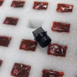
Top Pro-Grade Thermal Imaging Sensor Module: AI-Enhanced LWIR Solutions for Drones & DIY Tech
2026年6月23日
Thermal Camera Module Price Guide 2024: From DIY Kits to Pro Edge AI Solutions
For procurement officers, hardware integration engineers, and R&D specialists, selecting a thermal imaging core goes far beyond acquiring a component—it is a balancing act between sensor physics, thermal sensitivity, digital processing bottlenecks, and overall system yields. In 1800, Sir William Herschel discovered infrared radiation, laying the foundation for modern thermography. Today, the industrial market is flooded with choices, ranging from $100 entry-level micro-cores to rugged, high-resolution $5,000+ Edge-AI-powered Long-Wave Infrared (LWIR) engines. Calculating the true lifetime cost of integration requires an understanding of how sensor pitch, lens materials, calibration parameters, and processing pipelines drive up manufacturing costs. This comprehensive guide breaks down the core cost drivers of the thermal camera module price, details performance tiers, provides actual hardware specifications, and explores how to select the optimal LWIR or MWIR engine without overpaying for unnecessary specifications.
Table of Contents
- 👉 1. Core Physics & Economic Price Drivers
- • 1.1 Resolution, Pixel Pitch, and Sensor Wafer Yields
- • 1.2 Germanium Lens Physics and Chalcogenide Alternatives
- • 1.3 Radiometric Calibration and Pixel-Level Compensation
- 👉 2. Microbolometer Architecture & Core Technologies
- • 2.1 VOx vs. a-Si Infrared Detectors
- • 2.2 Uncooled LWIR vs. Cryogenically Cooled MWIR
- 👉 3. Interface Electronics & Processing Pipelines
- • 3.1 Digital Video Interfacing: MIPI, USB, CVBS, and SPI
- • 3.2 Edge AI Integration and Onboard ISP Pipelines
- 👉 4. Demystifying the Thermal Camera Module Price Matrix
- 👉 5. Real Hardware Showcases & Specifications Table
- 👉 6. Deep-Dive B2B Technical FAQ
1. Core Physics & Economic Price Drivers
1.1 Resolution, Pixel Pitch, and Sensor Wafer Yields
Here's the deal: the absolute biggest driver of your thermal camera module price is the physical size of that micromachined sensor array and how densely those micro-pixels are packed. We aren't dealing with your run-of-the-mill visible-light silicon CMOS sensors here. Those mass-produced visible sensors drop billions of sub-micron pixels onto dirt-cheap dies. Thermal sensors are a whole different beast. They rely on specialized suspended Wikipedia Microbolometers, which run on a design-matched Read-Out Integrated Circuit (ROIC). This is a complex micro-electromechanical system (MEMS) requiring specialized surface micromachining. In the shop, we look at these suspended pixels as tiny diving boards—each pixel is physically hung over the silicon substrate by microscopic dual-leg bridges. These legs thermally isolate the pixel, letting us measure tiny variations in active electrical resistance when infrared light warms it up.
When you sit down to compare sensor resolutions, keep in mind that the structural density and the total active surface area of the silicon substrate don't scale in a straight line. The physical costs ramp up exponentially:
- ⚙️ 160x120 array: Contains exactly 19,200 active pixels. Think of this as the bare-minimum target for basic close-range hot-spot checks.
- ⚙️ 256x192 array: Contains 49,152 active pixels. That is a massive 156% jump in spatial resolution over standard 160-cores, giving you a much tighter grip on object contours.
- ⚙️ 384x288 array: Contains 110,592 active pixels. This diagnostic-grade tier represents an extra 125% bump in spatial data compared to the 256x192 sweet spot.
- ⚙️ 640x512 array: Contains 327,680 active pixels. Now you are looking at a 566% increase in raw spatial data over the mid-range cores, unlocking clinical-grade visual analytics and long-distance perimeter safety.
As those sensor dimensions grow, things get tricky on the cleanroom floor. Raw semiconductor wafer yields drop like a stone. Fabricating microbolometers on large silicon wafers leaves them wide open to microscopic structural defects. A single tiny speck of dust or a minor physical imbalance on the wafer line can instantly kill an entire wide-format die (especially those roomier 640x512 cores). If a wafer only fits 100 large-format dies to begin with, even a minor defect density is going to send domestic yields straight into the scrap bin—way faster than if you were slicing up 1,000 tiny 80x60 dies. This brutal yield math explains why high-resolution thermal modules reject commoditization and carry premium price tags.
Look at the pixel pitch evolution, too. Moving from older, bulkier 17μm (micrometer) pixel pitches down to modern 12μm (and even bleeding-edge 10μm) allows chip foundries to squeeze more usable sensor dies onto a single wafer. That helps ease raw material costs, but it introduces major optical hurdles. When you shrink an individual pixel's physical surface area down to 12μm, it naturally captures fewer infrared photons. This means your electronic noise floor spikes instantly unless your engineering team spends a premium on high-end, ultra-low-noise readout circuits. Achieving clean performance and tight thermal sensitivity (low Noise Equivalent Temperature Difference, or NETD) on smaller pixel structures is why true high-performance 12μm cores still demand a serious premium.

1.2 Germanium Lens Physics and Chalcogenide Alternatives
When you are designing these systems, remember that standard optical glass (silicon dioxide) is completely useless here. Try shooting a thermal wave through a normal glass lens, and it acts like a brick wall—absorbing and blocking everything in the Long-Wave Infrared (LWIR) spectrum (8μm to 14μm). To get that thermal energy back to the microbolometer, design teams have to specify specialized optical materials. The industry gold standard is optical-grade crystalline Germanium (Ge).
Germanium is a phenomenal materials-science achievement for IR optics. It offers a sky-high refractive index of roughly 4.0 in the LWIR band, minimal optical dispersion, and serious physical toughness in harsh field conditions. But Germanium is a rare, hyper-expensive metalloid, and its raw market price fluctuates wildly. Grinding and polishing raw Germanium requires ultra-precise, single-point diamond turning (SPDT) machines to hit target optical profiles without fracturing the crystal structure. Because of this, a ruggedized, high-performance Germanium lens assembly can easily chew up to 35% of your entire thermal camera core's bill of materials (BOM).
If you are pinching pennies on a high-volume commercial build, you should look into Chalcogenide glass alternatives. This material is made of a mix of sulfur, selenium, and arsenic, and it can be directly hot-pressed into precision molds instead of requiring slow, costly diamond turning. This opens the door to high-speed molding pipelines that keep raw costs low. But watch out for the pitfalls: Chalcogenide has a visibly lower refractive index (hitting around 2.5 to 2.8), is physically more brittle, and struggles to handle extreme thermal shocks in the field without micro-fracturing. As an integrator, you have to decide if your deployment environment can get by on molded Chalcogenide class optics, or if you need to shell out for diamond-turned Germanium to survive the elements.
Don't overlook the optical aperture (the F-number), either. An F/1.0 lens pulls in double the thermal radiation of an F/1.4 lens. But keeping that F/1.0 rating while controlling aberrations means you need thicker, wider-diameter Germanium blanks and rigorous quality checks. That extra glass sends your optical subsystem costs upward in a hurry.
1.3 Radiometric Calibration and Pixel-Level Compensation
Here is a massive dividing line in the B2B marketplace: are you looking for basic "thermal visualization" cores (which generate eye-catching colorized hot/cold pictures but lack actual numeric data values) or true high-accuracy "radiometric" engines (which calculate the absolute temperature value for every single pixel in the frame)? Transforming an uncalibrated microbolometer into a field-ready radiometric instrument is a grueling, calibration-heavy engineering process.
Because microbolometers are highly sensitive structures, no two pixels are identical off the line. Every single pixel has its own unique electrical gain and offset profile. If you stream raw data straight from the sensor without fixing this, your display will look like a snowstorm of gray noise. To clean it up, production lines use a complex multi-step Non-Uniformity Correction (NUC) procedure. Manufacturers mount each core in a temperature-controlled environmental chamber, pointing them at laboratory-grade blackbody calibration sources across several thermal stages.
This painstaking step maps out complex multi-point correction tables that the module processes on the fly:
Where:
- V_out(i,j) represents the corrected electronic signal for pixel coordinates (i,j).
- G(i,j) is the specific gain correction multiplier stored in flash memory.
- Phi(i,j) is the raw incoming infrared radiative energy hitting the pixel.
- O(i,j) is the active offset value, which drifts as the sensor's internal temp changes.
To run these math pipelines, the core needs dedicated onboard storage and computing power—usually a low-power, high-speed FPGA or a specialized ARM microcontroller. On top of that, radiometric cores almost always include a physical mechanical shutter. Throughout operation, the core will briefly close this shutter to establish a uniform, known thermal baseline, updating the offset tables to compensate for internal heat buildup (this is called a shutter-NUC cycle). The added cost of that micro-motor, the machined shutter blade, the driver chip, and the lab labor adds up, directly impacting the final wholesale cost of your module.
2. Microbolometer Architecture & Core Technologies
2.1 VOx vs. a-Si Infrared Detectors
The uncooled LWIR thermal module market is dominated by two main materials for the active microbolometer layer: Vanadium Oxide (VOx) and Amorphous Silicon (a-Si). They represent very different engineering schools of thought when it comes to material costs and image processing demands.
| Technical Benchmark | Vanadium Oxide (VOx) Core | Amorphous Silicon (a-Si) Core |
|---|---|---|
| Temperature Coefficient of Resistance (TCR) | High (~ 2% to 3% per Kelvin) | Moderate (~ 1.5% to 2% per Kelvin) |
| 1/f Electronic Noise Characteristic | Very low; leads to extremely clean images | Somewhat higher; requires digital filtering |
| Fabrication & Scale Scalability | Requires dedicated MEMS processing steps | Highly compatible with standard CMOS steps |
| Thermal Time Constant Response | Fast response (typically 8ms to 15ms) | Slightly slower response (15ms to 22ms) |
| Typical Application Profiles | High-sensitivity defense, aerospace, UAVs | Industrial automation, building diagnostics |
Vanadium Oxide (VOx) is the undisputed performance leader for demanding tactical and high-sensitivity integrations. Its high TCR means even a fractional temperature shift in your scene creates a clean, readable signal. VOx sensors keep electrical "pink noise" (1/f noise) to a minimum, meaning they can achieve thermal sensitivities under 35mK without breaking a sweat. If you are tracking low-contrast objects in thick fog or scanning cold landscapes, a VOx core will resolve fine structures that an a-Si engine is likely to wash out.
On the flip side, Amorphous Silicon (a-Si) is highly compatible with the massive silicon semiconductor fabrication lines we use for mainstream electronics. Since it is easy to work with in standard silicon wafer fabs, you can scale a-Si production to massive volumes quickly. But because raw a-Si carries a noisier electrical profile, these modules place a heavy burden on your downstream processing. Your image processor has to run intensive spatial and temporal filtering algorithms to scrub the noise and deliver a clean image. This shift moves the performance burden from physical sensor materials over to advanced digital signal processing assets.
2.2 Uncooled LWIR vs. Cryogenically Cooled MWIR
In thermal design engineering, systems are divided into uncooled and cryogenically cooled modules. Uncooled thermal modules let the microbolometer sensor operate at ambient temperature with active stabilization provided by simple Thermoelectric Coolers (TECs) or heater elements. They are compact, draw minimal power, and require virtually zero periodic maintenance, making them ideal for long-term integration into portable devices, automated smart farms, and persistent security arrays.
But when you need maximum detection ranges, cooled Mid-Wave Infrared (MWIR) or Long-Wave cooled modules are unmatched. These advanced engines rely on Indium Antimonide (InSb) or Mercury Cadmium Telluride (MCT) focal plane arrays physically bolted to a miniature, high-frequency Stirling cryocooler. These mechanical coolers chill the sensor array down to a freezing 77 Kelvin (-196°C), almost completely dropping system thermal noise out of the picture. This allows cooled engines to hit sub-15mK thermal sensitivities.
This incredibly low noise floor allows cooled systems to run at ultra-fast frame rates, making them indispensable for tracking fast-moving targets without motion blur. They also utilize the 3μm to 5μm spectral window, which resists moisture absorption over long distances far better than the LWIR band. But cooled systems are a major budget commitment. Stirling cryocoolers are precision mechanical assemblies with finite mechanical life cycles (typically 5,000 to 15,000 running hours before they require gas recharging or seal maintenance), and they consume substantial power. For most standard B2B industrial projects, uncooled LWIR cores remain the most practical and cost-effective path forward.
3. Interface Electronics & Processing Pipelines
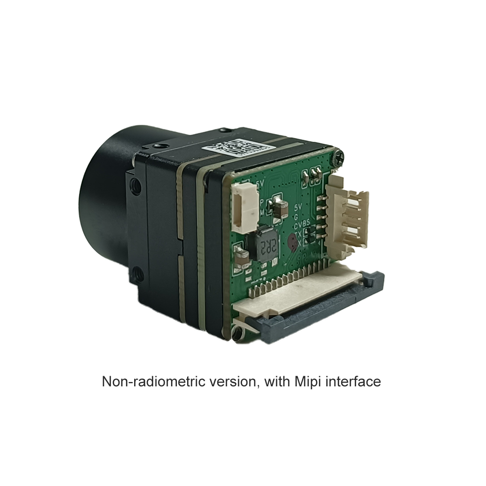
3.1 Digital Video Interfacing: MIPI, USB, CVBS, and SPI
A major design check when specifying a thermal imaging sensor core is the digital interface protocol. This choice determines the hardware complexity, processing latency, and processor choice for the host system:
- ⚙️ MIPI CSI-2 (Mobile Industry Processor Interface): The absolute standard if you are designing a sleek system around high-power System-on-Chips (SoCs) like the NVIDIA Jetson, Raspberry Pi Compute Module, or NXP i.MX8. MIPI streams uncompressed digital pixels with close to zero latency, all while keeping power draw exceptionally low. The catch is that writing custom MIPI drivers for your specific kernel can take serious software development time.
- ⚙️ USB 3.0 / USB Type-C: Extremely popular for quick prototyping and direct-to-PC interfaces. Many modern cores come pre-configured with standard USB Video Class (UVC) drivers, making them plug-and-play. This saves massive engineering hours on driver development, but USB connectors lack rugged, vibration-proof industrial locking mechanisms and run hotter than native serial lanes.
- ⚙️ CVBS (Composite Video Baseband Signal): This legacy analog connection is still very common in drone gimbals and long-range analog CCTV systems. It provides zero-latency analog video streams across coaxial lines. The downside is that you lose the raw digital data, meaning your downstream processors can't run precise radiometric analysis on the pixels.
- ⚙️ SPI (Serial Peripheral Interface): The go-to interface if you are integrating basic, low-resolution cores (like 80x60 or 160x120) with low-power microcontrollers like STM32 or ESP32 chips. SPI is simple to wire up and highly cost-effective, but it doesn't have the bandwidth to transfer rich, high-resolution, high-frequency thermal video without dropping frames.
3.2 Edge AI Integration and Onboard ISP Pipelines
Modern thermal modules don't just dump raw pixel values onto your processor. They carry onboard Image Signal Processors (ISPs) or FPGAs that do the heavy lifting before the data ever hits your main controller. These internal pipelines run several key image optimization algorithms:
- ✅ Dynamic Range Compression (DRC): Compresses wide 14-bit thermal sensor data into high-contrast 8-bit gray or colorized palettes, ensuring subtle details are visible in cold environments even when hot targets are present.
- ✅ Digital Detail Enhancement (DDE): High-frequency spatial filters that sharpen edges and raise structural features, making it easier for human observers and automated tracking models to identify targets.
- ✅ 3D Noise Reduction (3DNR): Analyzes both spatial and temporal noise profiles to clean up thermal video without introducing ghosting or trailing artifacts during fast pans.
What is really changing the game right now is the integration of Edge AI accelerator chips directly onto the module's PCB. These built-in micro-NPUs are trained to run lightweight neural networks like Tiny-YOLO. Instead of sending raw, heavy video files back to a central server, these smart modules can detect humans, identify hot bearings, detect security breaches, and locate fires locally. This onboard intelligence reduces data transmission bandwidth, making it highly valuable for remote, solar-powered security grids and distributed industrial networks.
4. Demystifying the Thermal Camera Module Price Matrix
To help system integrators and purchasing departments balance engineering needs with their budgets, the table below maps out the thermal camera module price market across three functional tiers:
| Market Tier | Expected Unit Cost | Target Specs (Resolution/NETD) | Optical / Interface Configuration | Common B2B Use Cases |
|---|---|---|---|---|
| Low-End Hobbyist / Entry Integration | $100 to $300 USD | 80x60 to 256x192 NETD: ≤ 50mK to 60mK Frame rate: typically 9Hz |
Fixed-focus molded Chalcogenide lenses; simple SPI or basic USB outputs | Consumer gadgets, smart home appliances, rudimentary educational setups |
| Industrial Component / OEM Standard | $400 to $1,200 USD | 256x192 to 384x288 NETD: ≤ 40mK @ 25°C Frame rate: 25Hz to 50Hz |
High-transmission Germanium lenses; native parallel bus, MIPI, or USB | UAV drone gimbals, smart building maintenance, automated machine vision |
| Premium Professional / Tactical / Edge AI | $1,500 to $5,000+ USD | 640x512 to 1024x768 NETD: ≤ 25mK to 30mK Frame rate: up to 60Hz |
Motorized-focus/continuous-zoom Germanium optics; precision-calibrated radiometry | Border patrol, tactical targeting, complex industrial failure analysis |
One major variable you must factor into your pricing is export licensing. High-frame-rate thermal modules (anything operating above 9Hz) are classified as dual-use military components by many governments. This designation triggers strict end-user-undertaking reviews and export license protocols, which adds administrative overhead and processing time to your procurement. If your use case doesn't require ultra-smooth fluid video, choosing a 9Hz core will bypass many export regulations, lower your compliance burden, and reduce your physical purchase price.
5. Real Hardware Showcases & Specifications Table
For engineering teams working out physical layout constraints and structural mounting options, let's look at the mechanical and electrical specifications of our targeted uncooled cores:
| Technical Attribute | Mini 256 Uncooled LWIR Module | Uncooled Mini 384*288 Drone Module |
|---|---|---|
| Sensor Technology | Uncooled LWIR, similar to DJI Mine Detection specs | High-precision MINI active-temperature online imager |
| Native Active Resolution | 256 x 192 pixels (High sensitivity) | 384 x 288 pixels (Advanced density) |
| Thermal Sensitivity (NETD) | Ultra-clear performance detectors | High-sensitivity high-precision detector |
| Imaging Capabilities | Uniform thermal output with absolute radiometry | True online high-accuracy temperature measurements |
| Digital/Analog Interface Options | Direct processing stream integration parameters | Multiple physical digital interfaces + analog support |
| Primary System Integrations | Buried mine detection, compact UAV mounts | Robotics, machine vision, UAV airborne gimbals, equipment diagnostics |
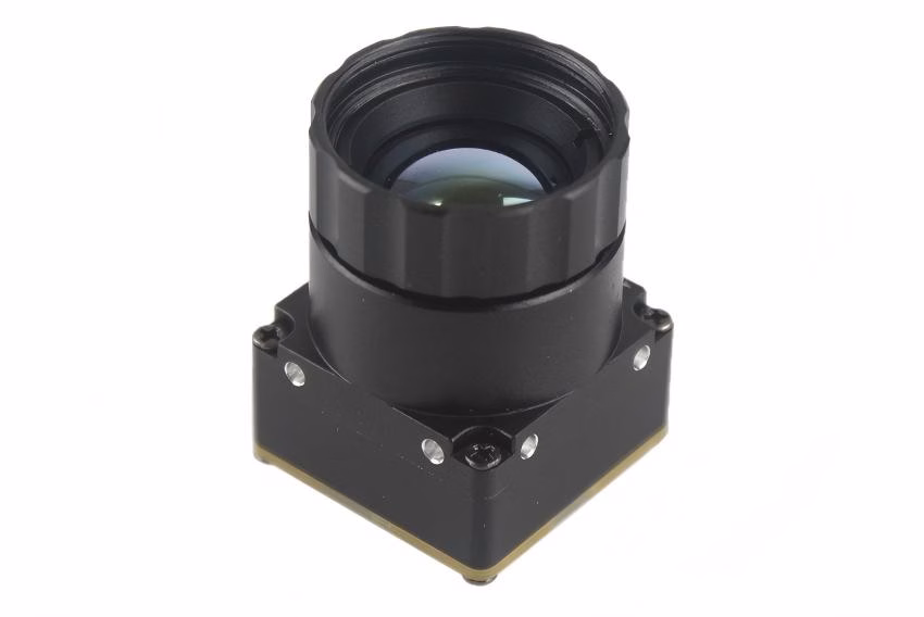
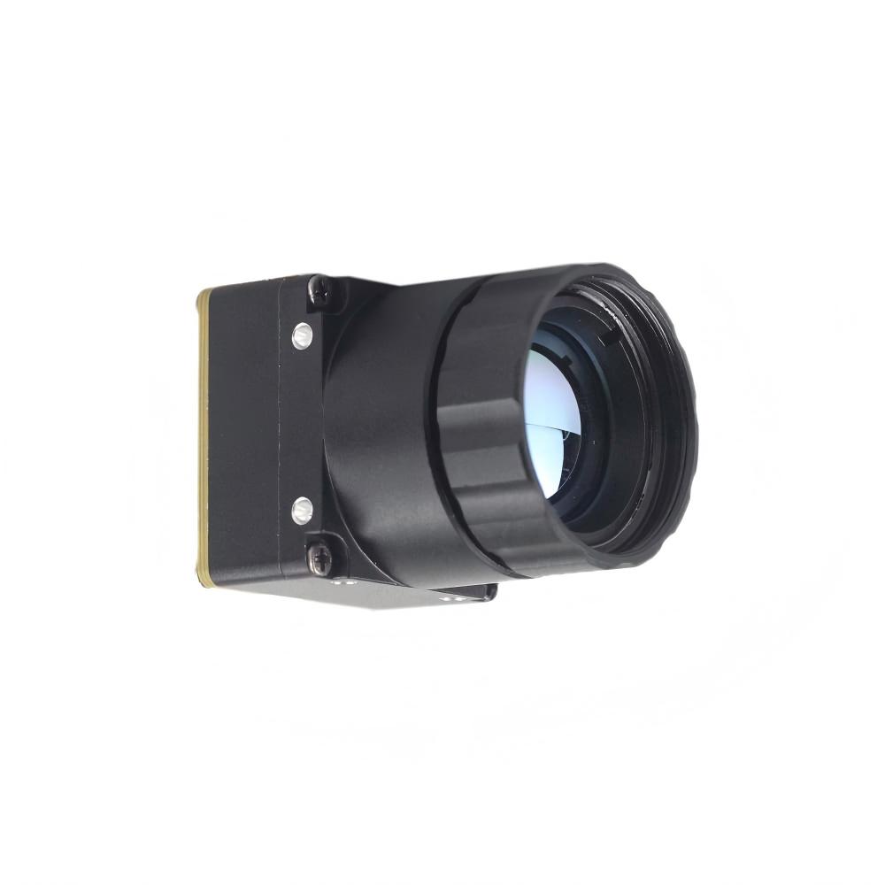
Detailed Showcase: Mini 256 Uncooled LWIR Thermal Imaging Camera Module
If you are trying to cut down on weight without sacrificing thermal performance, our Mini 256 sensor is a perfect fit. It is engineered with a small footprint to deliver a balanced combination of optical clarity and lightweight design. It streams high-contrast thermal patterns alongside calibrated radiometric data, making it an excellent choice for specialized integrations like localized mine detection and remote robotics.
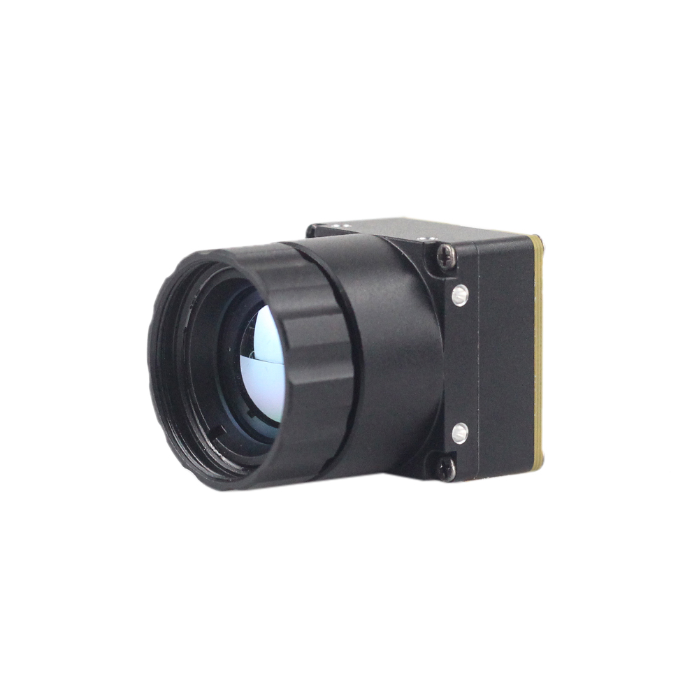
The Mini 256 shines in handheld security systems, remote industrial machinery monitoring, and micro UAV payloads. It finds the sweet spot between high sensitivity and a compact form factor, giving system integrators a reliable, cost-effective uncooled core that interfaces smoothly with standard embedded processors.
View Product Details & Pricing ➔
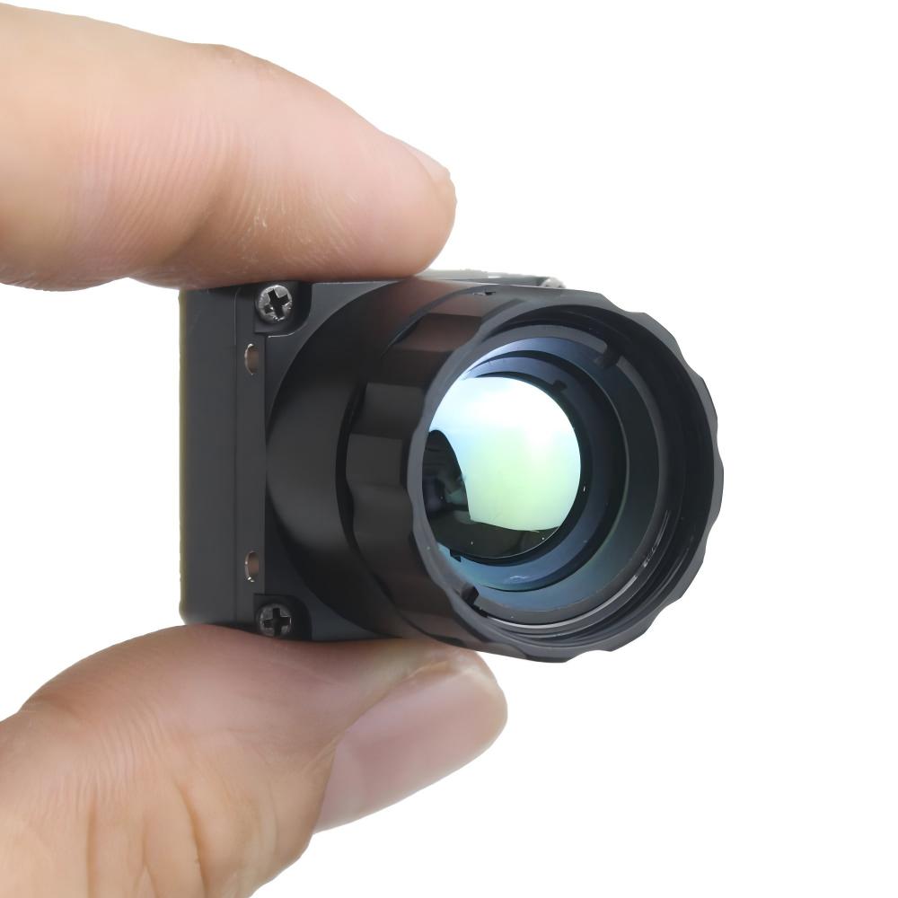
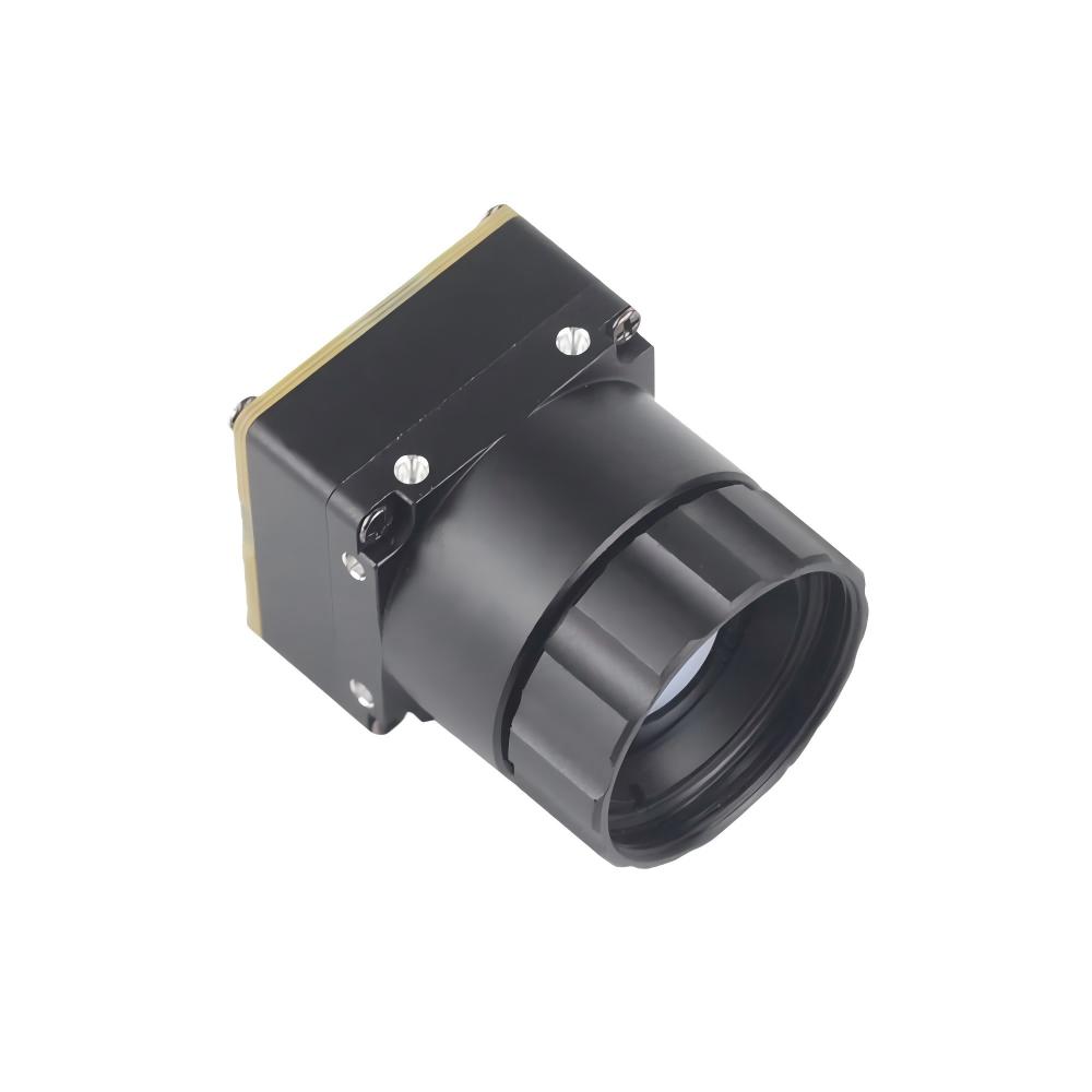
Detailed Showcase: Uncooled Mini 384*288 Thermal Camera Module for Drones
Stepping up to the Mini 384*288 core delivers a major performance boost, offering physical thermal sensitivity, higher spatial resolution, and broader interface flexibility. This rugged module is optimized for industrial drone gimbals, smart factory monitoring, robotic crawlers, and electrical grid tracking.
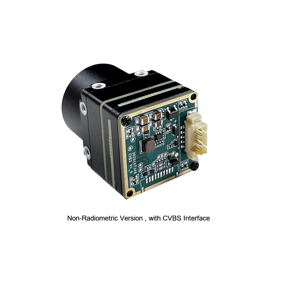
This core supports both analog CVBS and versatile digital outputs, allowing it to connect directly to analog video transmitters or high-end digital image capture devices. This interface flexibility lets you transition between legacy analog pipelines and modern, high-precision digital processing systems as your project demands.
View Product Details & Pricing ➔

6. Deep-Dive B2B Technical FAQ
Why is there such a massive price gap between a $200 and a $3000 thermal module?
When you step up to a $3,000 professional core, you are looking at a 640x512 VOx sensor built on a tight 12μm or 10μm pitch. Squeezing that many pixels onto a wafer drives down yields dramatically, since a single micro-fleck of dust during lithography can ruin a high-resolution die. These pro cores are paired with high-aperture (F1.0) diamond-turned Germanium lenses, which are incredibly expensive. Finally, they require labor-intensive environmental chamber calibration. This ensures their internal lookup tables run real-time radiometric calculations, providing absolute, highly accurate temperature measurements across every pixel in the frame.
Can I get a high-res thermal module for a Raspberry Pi or Arduino project under $200?
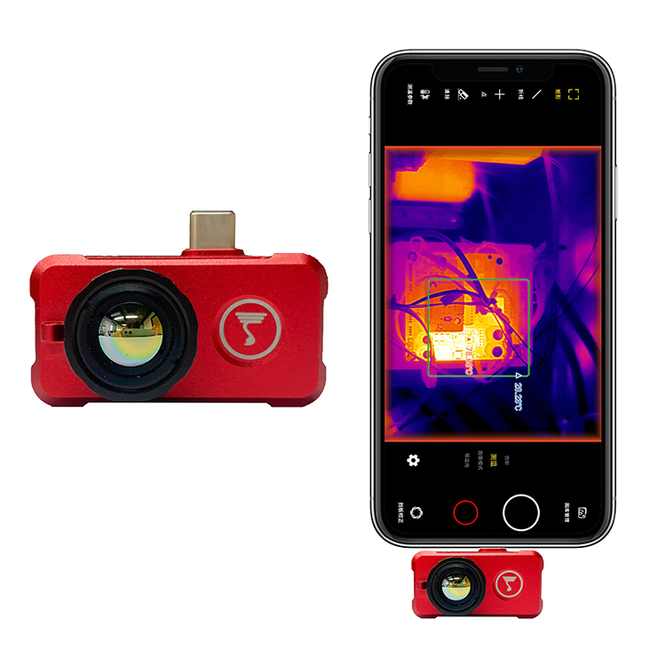
If you are on a tight budget, choosing a 256x192 module is your best bet. It delivers 49,152 active pixels of rich radiometric data while staying highly cost-effective. These modules are easy to test with direct USB connections or custom serial links. If you need step-by-step guidance on integration code libraries and platform control setups, head over to our Mobile Thermal Imager App and User Manual Page, which details host device communications.
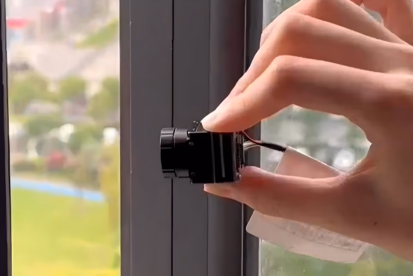
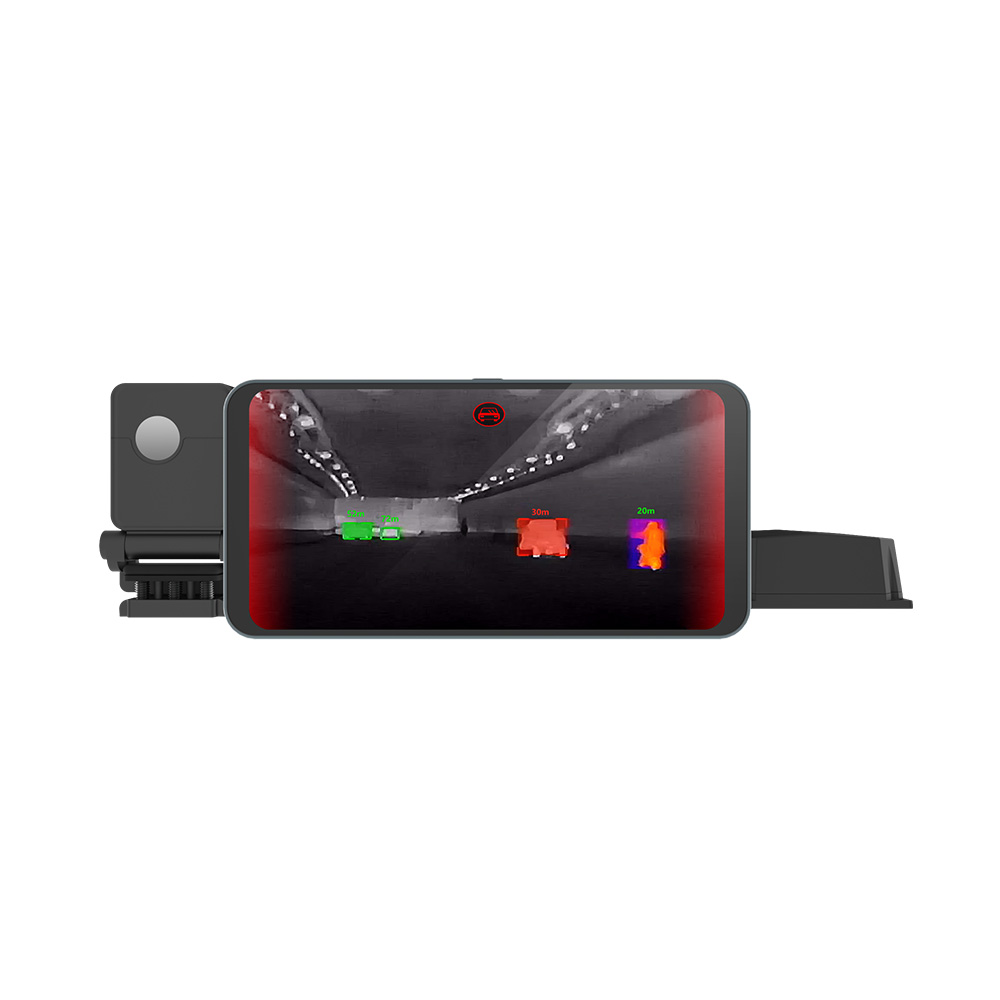
What makes a thermal module 'drone-ready' and does it increase the price?
When a drone climbs, it encounters rapid ambient temperature drops and strong wind cooling across the lens. Without active compensation, this thermal drift degrades imaging accuracy, causing the sensor readings to wander. Drone-ready cores overcome this using real-time thermal recalibration and custom shutter algorithms to maintain clear, accurate video during flight. To explore our design processes and OEM manufacturing standards, check out our About Us Page. If you are ready to purchase a system evaluation kit, head over to our secure Checkout Portal to view raw core options.
📚 References & Further Reading
- Industry Standard: Wikipedia Thermography Physics
- Core Technology Guide: Wikipedia Microbolometer Solid-State Geometries
- Related Guide: Mobile Thermal Imager Q3 Series Control App and SDK Manuals