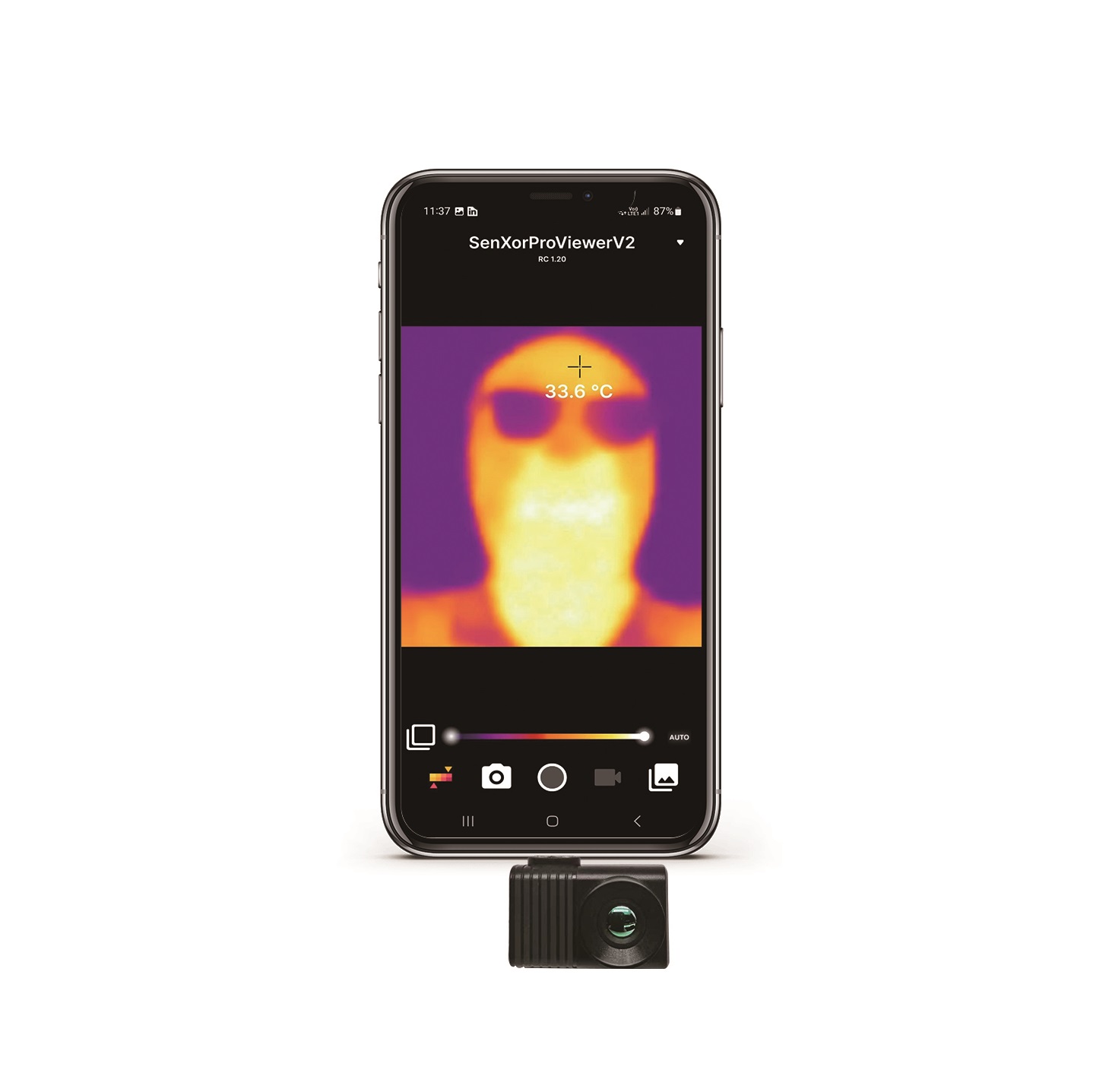
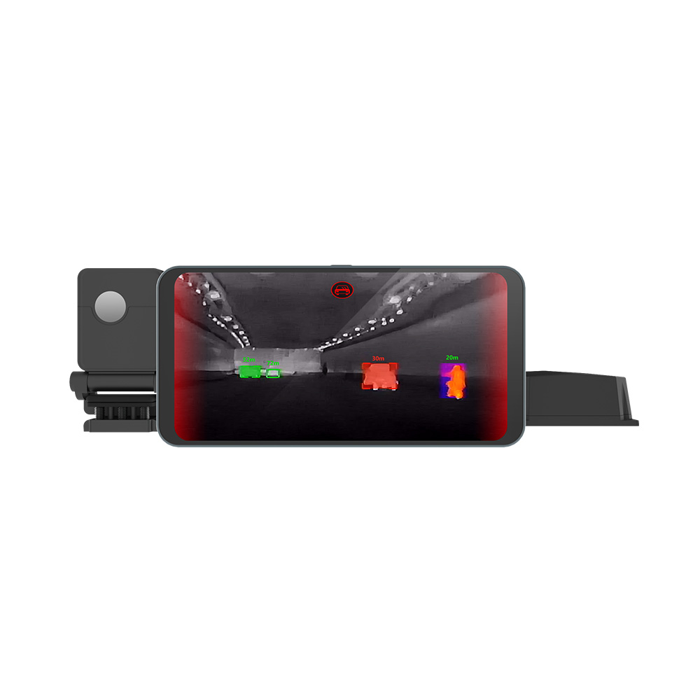


Thermal Camera Core OEM: High-Resolution LWIR Modules for Drones & Vision Systems
2026年9月4日
Thermal Module SDK for Integration: Developer Guide for Embedded AI & Radiometry
2026年9月7日
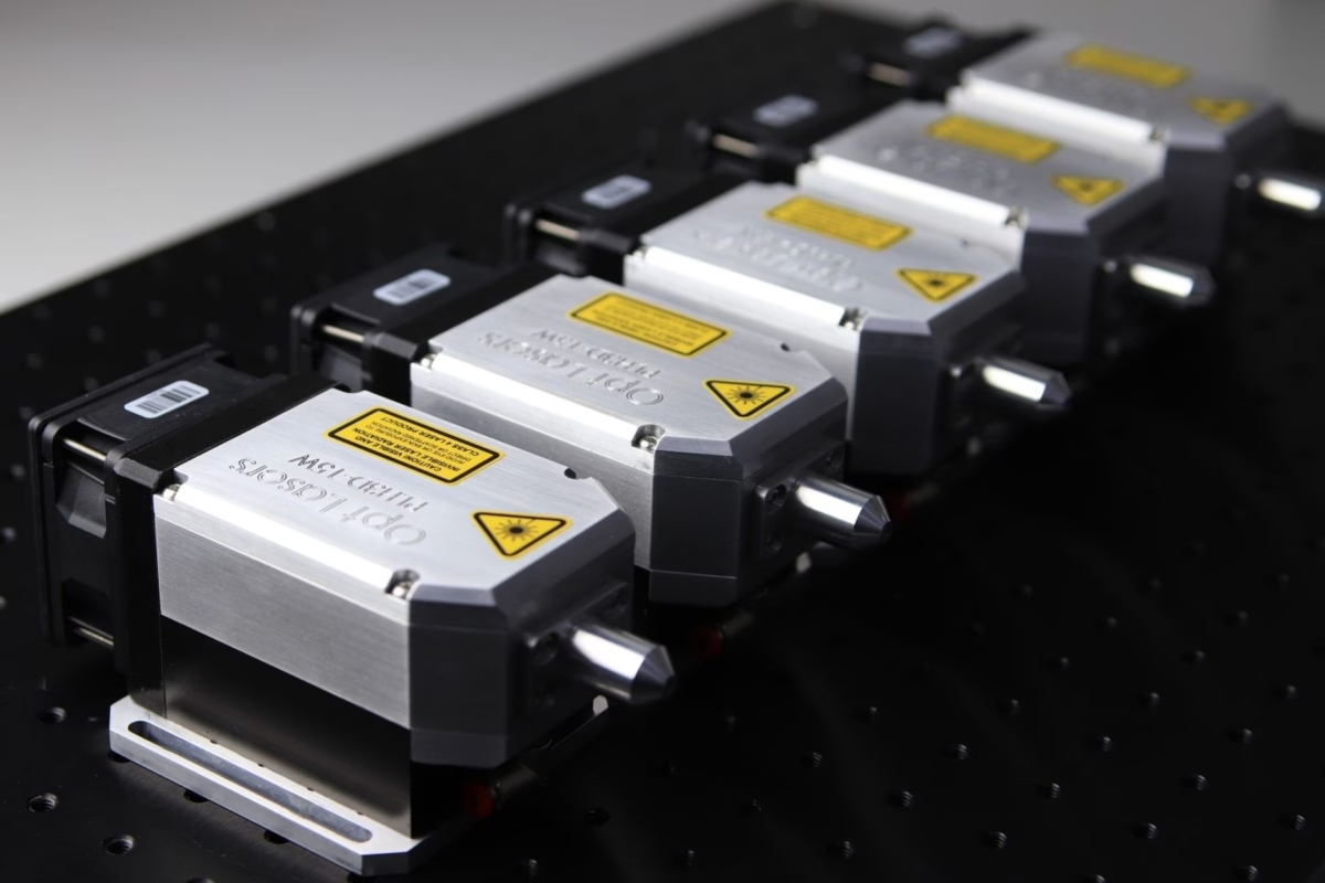
Custom Thermal Imaging Module ODM: High-Performance LWIR Cores & Edge AI Integration
Here’s the deal: anyone who has tried cramming a generic commercial off-the-shelf (COTS) thermal camera into a tight carbon-fiber drone airframe or a tactical weapon sight knows the headache. You're immediately hit with severe Size, Weight, and Power (SWaP) penalties, rigid optical barrels that don't match your target distance, and proprietary firmware black-boxes that refuse to spit out raw digital data. Catalog cameras are fine for lab benches or routine industrial audits, but they fall apart fast when you need deterministic real-time targeting, sub-surface mine clearance, or micro-stabilized airborne gimbals. When you hit that wall, you have to look past the distributor catalog and partner with a dedicated thermal imaging module ODM (Original Design Manufacturer) that can cut metal, spin bare-metal PCBs, and burn custom FPGA logic directly around your mission profile.
Engineering an uncooled long-wave infrared (LWIR) platform isn't just about sticking a sensor behind a lens. It requires micro-level control across half a dozen physical disciplines: non-uniformity correction (NUC), high-vacuum focal plane array (FPA) packaging, parasitic thermal drift stabilization, and deterministic edge signal processing. An ODM engagement empowers payload designers to ditch bloated legacy hardware. We're talking about dropping the physical footprint down to 21×21 mm, terminating raw 14-bit radiometric streams over native MIPI-CSI2 or USB-C interfaces, and custom-turning Germanium optics to nail an exact Field of View (FOV). In this guide, we break down the hardware physics, SWaP-C optimization strategies, edge AI integration pipelines, and practical manufacturing workflows needed to build enterprise-grade infrared vision systems that survive in the field.
Table of Contents
- 👉 1. Advanced LWIR Core Architecture & Uncooled VOx Sensor Physics
- 👉 2. SWaP-C Engineering: Micro-Scale Integration Strategies
- 👉 3. Embedded Edge AI Pipelines & Hardware Signal Processing
- 👉 4. Electro-Optical Configurations & Physical Interface Customization
- 👉 5. The Industrial ODM Workflow: From System Concept to Scaled Production
- 👉 6. Real-World Product Showcase: Industrial LWIR Cores
- 👉 7. Comprehensive Technical FAQ
1. Advanced LWIR Core Architecture & Uncooled VOx Sensor Physics
Operating inside the 8µm to 14µm long-wave infrared window requires direct manipulation of thermal radiation invisible to standard CMOS image sensors. In high-end defense systems, you’ll find cryogenically cooled sensors like Indium Antimonide (InSb) or Mercury Cadmium Telluride (MCT). They’re sensitive, sure, but their Stirling cryocoolers are noisy, heavy, power-hungry, and come with a Mean Time Between Failures (MTBF) that limits field lifespan. For tactical UAVs, dismounted optics, and industrial monitoring, uncooled microbolometers are the practical choice. In modern ODM lines, the industry has shifted away from Amorphous Silicon (a-Si) in favor of thin-film Vanadium Oxide (VOx). In the shop, VOx consistently beats a-Si on two critical metrics: a higher Temperature Coefficient of Resistance (TCR, generally running -2% to -3% per Kelvin) and significantly lower 1/f flicker noise. This results directly in lower Noise Equivalent Temperature Difference (NETD), yielding superior thermal contrast across low-gradient environments.
The signal path starts at the micro-bridge. Incident thermal radiation passes through a protective optical window and hits an array of microbolometer pixels suspended on microscopic silicon legs over a high-vacuum Readout Integrated Circuit (ROIC). Each pixel absorbs infrared energy, heating up slightly and changing its electrical resistance. The ROIC integrates this resistance change using low-noise capacitive transimpedance amplifiers, converting micro-Kelvin thermal differentials into voltage levels. High-speed multi-channel analog-to-digital converters (ADCs) digitize the signal directly on the focal plane before handing off the raw stream to an adjacent FPGA or ASIC for processing, calibration, and edge inferencing.
1.1 Microbolometer Mechanics, 12µm Pixel Pitch, and Thermal Time Constants
The mechanical structure of each microbolometer pixel is a tiny engineering marvel: an ultra-thin absorber plate held above the substrate by narrow micro-machined legs. These legs isolate the pixel thermally, providing a high thermal resistance that allows minimal absorbed radiation to create a measurable jump in temperature. The trade-off is the thermal time constant—how quickly the pixel heats up and cools back down. If the time constant is too high, high-speed pans look like a blurry mess; if it’s too low, thermal sensitivity drops. For high-frame-rate 50Hz/60Hz aerial tracking or ballistic targeting, balancing that time constant between 8ms and 12ms is essential to eliminate ghosting artifacts without losing faint thermal signatures.
Shifting down to a 12µm pixel pitch from legacy 17µm or 25µm nodes is where modern SWaP improvements originate. Shrinking the pixel pitch slashes the physical sensor die area by more than 50% for standard resolutions like 640×512 or 256×192. That footprint reduction cascades through the entire optomechanical assembly: smaller dies need shorter optical focal lengths to hit the exact same Instantaneous Field of View (IFOV). That means your front Germanium elements get smaller, the lens barrel gets shorter, and the mass hanging off your gimbal drops dramatically.
1.2 Radiometric Precision, Non-Uniformity Correction (NUC), and Shutterless Operation
Every single pixel on an uncooled focal plane array comes off the fab line with tiny manufacturing variances in raw resistance, thermal dissipation, and amplifier response. Without correction, that variation creates fixed-pattern noise (FPN), making the video feed look like it's covered in static. An ODM engineering partner tackles this fixed pattern noise through multiple algorithmic stages:
- ⚙️ Two-Point Non-Uniformity Correction (NUC): Computes unique gain and offset matrices per pixel using multi-temperature blackbody chambers, mapping non-linear microbolometer response into a uniform digital gray-level spectrum.
- ⚙️ Mechanical Shutter Calibration: Actuates a calibrated internal paddle to drop an isothermal surface across the sensor plane, resetting the baseline offset table to clear dynamic thermal drift caused by changing ambient conditions.
- ⚙️ Shutterless Algorithmic NUC (SBNUC): For high-vibration drone platforms, missile seekers, and targeting scopes, mechanical shutters risk mechanical failure or momentarily freeze critical targeting video streams. Advanced ODM firmware incorporates scene-based non-uniformity correction (SBNUC). SBNUC models core spatial frequency variations alongside internal temperature thermistor readings to continuously drift-correct the active frame buffer without physical optical occlusion.
- ⚙️ Absolute Radiometric Mapping: Encodes true temperature telemetry directly into 14-bit or 16-bit metadata per pixel, calibrated across standard ranges (-20°C to +150°C) and extended high-temperature industrial scales (up to +550°C or higher).
2. SWaP-C Engineering: Micro-Scale Integration Strategies
When you're designing sub-systems for Class 1 micro-drones, soldier-worn gear, or distributed industrial IoT clusters, SWaP-C (Size, Weight, Power, and Cost) dictates every design choice. In aerial payloads, every single extra gram cuts flight time by seconds. At the same time, poor electrical efficiency drains battery banks and radiates parasitic heat back into the optical engine, blinding the infrared sensor with internal thermal noise.
Solving SWaP-C isn't about using smaller screws; it demands treating the mechanical chassis, electronics, and optical stack as a single thermal engine. Rather than stacking multiple generic daughtercards with bulky board-to-board connectors, an experienced ODM merges the detector, readout, and power systems onto monolithic high-density boards designed to conduct heat away from the microbolometer.
2.1 Miniaturization Dynamics: Achieving the 21×21 mm Micro-Core Footprint
Getting a thermal core down to a miniature 21×21 mm profile requires high-density interconnect (HDI) routing, rigid-flex substrates, and wafer-level packaging (WLP). Traditional thermal camera designs rely on bulky ceramic or metal-can vacuum packages alongside discrete processing boards. An industrial ODM strips that excess mass away:
- ⚙️ Wafer-Level Packaging (WLP): Instead of sealing individual detectors in machined metal packages, WLP seals thousands of microbolometer dies simultaneously under high vacuum at the wafer level using silicon cap wafers. This shaves millimeters off the focal plane z-height.
- ⚙️ Direct Surface-Mount Integration (SMT): The detector mates straight onto the primary rigid-flex board, eliminating heavy pin sockets, lowering circuit loop inductance, and resisting mechanical shock.
- ⚙️ Dual-Purpose Aircraft Alloys: The outer housing is machined from thin-wall 6061-T6 hard-anodized aluminum or magnesium alloy. It serves a dual role: providing structural rigidity while functioning as an optical bench that holds back focal length (BFL) rock-solid across mechanical vibration.
2.2 Thermal Dissipation Modeling and Power Budgets under 1.0W
Uncooled microbolometers measure micro-Kelvin changes. If your onboard FPGA, DC-DC buck converters, or microcontroller radiate heat unevenly into the chassis, the detector registers that parasitic internal heat as real scene data. This creates ugly thermal gradients across the output image.
Keeping continuous operational power draw below 1.0W while operating across -40°C to +80°C demands careful circuit layout:
- ⚙️ Low-Noise Switching Architecture: Dynamically switched, low-noise power rails isolated by LDO regulators prevent switching hash from corrupting the ROIC's ultra-sensitive pixel-sampling clock.
- ⚙️ Isolated Copper Heat Planes: Internal PCB ground planes are thermally split, channeling processing heat away from the sensitive FPA face and shunting it toward the rear mounting block.
- ⚙️ Passive Chassis Conduction: Precision-milled thermal pads on the core's rear housing route heat directly into the host platform's structural frame—such as a drone's carbon arms or an aluminum enclosure—avoiding the need for noisy, failure-prone cooling fans.
3. Embedded Edge AI Pipelines & Hardware Signal Processing
Look, you can't just feed raw 14-bit thermal video into an off-the-shelf convolutional neural network and expect clean detections. Incident LWIR radiation naturally has low scene contrast compared to visible-light optics. An effective ODM module requires a hardware-accelerated image signal processor (ISP) built right next to the sensor engine to handle contrast enhancement and noise reduction before the frames ever touch a display or host CPU.
The signal chain transforms wide-dynamic-range radiometric data into high-contrast visual feeds or standardized tensor arrays. This hardware pipeline handles defect pixel concealment, real-time gain-offset calibration, spatial-temporal noise filtering, and dynamic range compression. It packs 14-bit data down into human-readable 8-bit streams without flattening low-contrast edge details.
3.1 FPGA/ISP Image Pipelines: DDE, 3D Noise Reduction, and Histogram Equalization
To run deterministic processing without blowing your power budget, custom modules implement fixed-function hardware pipelines running inside low-power FPGAs or dedicated ASICs with sub-20ms latency:
- ⚙️ Digital Detail Enhancement (DDE): This spatial filtering algorithm splits incoming frames into high-frequency detail channels (edges, target contours, small structural features) and low-frequency base channels. By boosting the high-frequency detail before recombining, targets like personnel or buried items jump out against flat background terrain.
- ⚙️ 3D Temporal Noise Reduction (3D-TNR): Analyzes pixel intensity over time to eliminate random Gaussian noise. Dynamic motion-detection flags prevent 3D-TNR from blurring the edges of high-speed moving targets.
- ⚙️ Adaptive Histogram AGC: Raw scenes encompass up to 16,384 discrete digital levels (14-bit), but standard monitors and simple vision models only handle 256 levels (8-bit). Adaptive AGC clusters gray-level allocation around active thermal signatures while discarding empty, uninformative thermal bands.
3.2 Edge Acceleration: Interfacing with OpenCV and Heterogeneous Neural Compute Engines
Modern remote payloads require fast, on-device classification. Relying on an RF datalink to stream raw video down to a ground station for inferencing introduces lag and risks RF jamming. Customized thermal cores can output synchronous, low-latency raw frames straight into embedded carrier boards, such as hardware built around Seeed Studio edge computing modules.
Running computer vision libraries like OpenCV on an onboard Linux or RTOS host allows payloads to isolate hot spots, run edge-detection routines, and execute optical tracking loops locally. By pairing V4L2 kernel-level drivers with streamlined C/C++ SDKs, the camera's linear radiometric stream maps directly into TensorRT-optimized neural nets (such as custom YOLO or SSD backbones). That enables real-time target recognition at native 50Hz/60Hz frame rates without stalling the host processor.
For a detailed breakdown of how low-noise processing pipelines maintain micro-details during practical deployment, take a look at this video analysis of uncooled LWIR 640 thermal camera modules.
4. Electro-Optical Configurations & Physical Interface Customization
A high-performance thermal engine is useless if it's paired with mismatched optics. Optical aperture design directly governs the Johnson Criteria performance of your system—dictating whether a target is a mere speck (Detection), an identifiable shape (Recognition), or an unambiguous object (Identification) at a given distance.
Designing optics for the long-wave infrared spectrum is fundamentally different from designing visible-light lenses. Standard optical glasses are completely opaque to LWIR photons. Engineers must use specialized crystalline or chalcogenide materials, cutting and coating them to maximize light transmission while accounting for thermal focus drift.
4.1 Germanium vs. Chalcogenide Optical Trains: Continuous vs. Prime Lenses (5mm to 150mm)
Selecting the right optical material is a balance of optical transmission, thermal stability, and manufacturing cost:
- ✅ Monocrystalline Germanium (Ge): The industry standard for high-end optical systems. It features a high refractive index (n ≈ 4.0) and very low dispersion. Finished with high-durability Anti-Reflective (AR) or Diamond-Like Carbon (DLC) hard coatings, Germanium lenses withstand harsh airborne grit and saltwater environments.
- ✅ Chalcogenide Glass: An engineered amorphous material composed of sulfur, selenium, and tellurium. Unlike Germanium, which must be diamond-turned, Chalcogenide optics can be precision-molded at scale. This lowers high-volume production costs while offering optical characteristics that make athermalizing the lens barrel much simpler.
A capable ODM maintains internal cleanroom tooling to assemble, align, and collimate wide varieties of focal lengths:
- ⚙️ Wide-Angle Prime Optics (5mm to 9mm): Ideal for close-in indoor searches, blind-spot clearance, and obstacle avoidance systems on autonomous mobile robots (AMRs).
- ⚙️ Mid-Range Prime Optics (13mm, 18mm, 35mm): The workhorse configuration for short-to-medium range drone payloads, building inspection platforms, and perimeter security mounts.
- ⚙️ Long-Range Surveillance Optics (50mm, 75mm, 100mm, 150mm): Large-aperture telephoto lenses built for maximum standoff range in coastal surveillance, counter-UAS suites, and border interdiction platforms.
If you're integrating these optical components into complete field systems, check out this multi-functional infrared night vision platform.
4.2 High-Throughput Interfacing: MIPI-CSI2, USB UVC, Parallel CMOS, and Custom Carrier Boards
Payload architectures vary, and forcing every design to use an off-the-shelf interface board adds unnecessary weight and points of failure. An ODM adapts the pinout and electrical bus directly to your host processor:
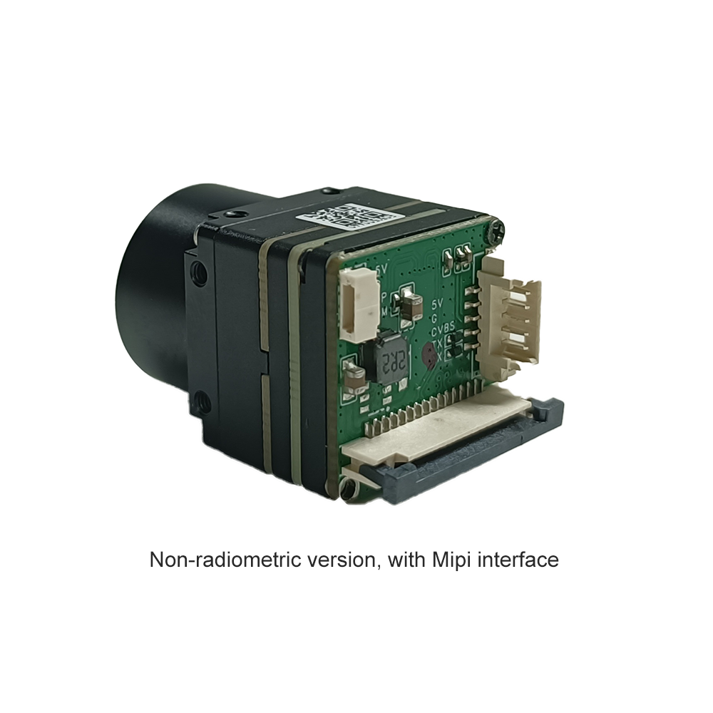
- ⚙️ MIPI-CSI2: The preferred interface for embedded compute modules (NVIDIA Jetson, NXP i.MX8, Rockchip). Transmits raw 14-bit data straight into the host’s direct memory access (DMA) buffers with minimal CPU overhead and ultra-low latency.
- ⚙️ USB 2.0 / USB-C (UVC Protocol): Perfect for plug-and-play connections to x86 mission computers and rapid test setups. The firmware can interleave standard 8-bit YUV/RGB frames with private 14-bit radiometric data over a single endpoint.
- ⚙️ DVP / Parallel CMOS: A lean interface for microcontrollers and specialized digital signal processors (DSPs) that need pixel-clock, line-valid, and frame-valid signals without packet overhead.
- ⚙️ Application-Specific Carrier Boards: Custom I/O boards replace generic breakout adapters, packing in power regulation (3.3V–18V), auxiliary telemetry inputs for laser rangefinders, IMU arrays, or rugged micro-circular locking connectors (like Hirose or Glenair).
5. The Industrial ODM Workflow: From System Concept to Scaled Production
Moving a thermal imaging core from a clean CAD drawing to a qualified hardware component demands rigorous process control. Unlike purchasing off-the-shelf units, an ODM relationship uses a structured stage-gate validation methodology to eliminate design risks, optimize assembly yield, and avoid supply bottlenecks before high-volume manufacturing begins.
This process systematically steps through architectural definition, rapid prototyping, firmware customization, and comprehensive environmental testing. Optical ray tracing, finite element analysis (FEA), and real-time blackbody radiometric tuning are maintained in continuous feedback loops throughout development.
5.1 Stage-Gate Verification: Prototype Bring-Up, MTBF Testing, and Environmental Stress Screening
Field payloads have to handle thermal shock, high electrical noise, and constant physical vibration without mechanical degradation or optical misalignment:
- ⚙️ Finite Element Analysis (FEA): Simulates mechanical resonance across the chassis to prevent internal microphonic noise from coupling into the sensitive, high-gain ROIC.
- ⚙️ Environmental Stress Screening (ESS): Prototypes undergo thermal cycling from -40°C to +80°C in environmental test chambers, weeding out cold solder joints and testing for thermal expansion mismatches in bonded lenses.
- ⚙️ Multi-Axis Shock & Vibration: Modules are subjected to rigorous shaker profiles simulating high-G projectile discharge, airframe harmonic vibration, and rough off-road transport, meeting MIL-STD-810H standards.
5.2 Regulatory Compliance, Optical Calibration, and End-of-Line Blackbody Tuning
Solid radiometry relies on disciplined factory calibration. Production lines use automated optical testing stations to ensure every unit performs consistently:
- ⚙️ Automated Multi-Point Blackbody Rigs: Arrays of traceable, high-emissivity (emissivity ≥ 0.995) blackbody plates sweep the thermal core's response curves across wide temperature intervals.
- ⚙️ Bad Pixel Replacement (BPR) Mapping: Identifies dead or erratic pixels at the factory level, permanently storing geometric interpolation offsets inside onboard flash memory.
- ⚙️ Modulation Transfer Function (MTF) Verification: Automated optical collimators measure edge-to-edge optical resolution across the focal plane, confirming focus and alignment before shipping.
For a detailed look at how to navigate OEM/ODM thermal module integration, read through our engineering guide to OEM thermal integration.
6. Real-World Product Showcase: Industrial LWIR Cores
To give you an idea of the physical architectures achievable through focused ODM development, here are two production-ready micro-cores designed for UAV platforms, landmine detection suites, and tactical optronics assemblies.
Mini 256 Uncooled LWIR Thermal Camera Module
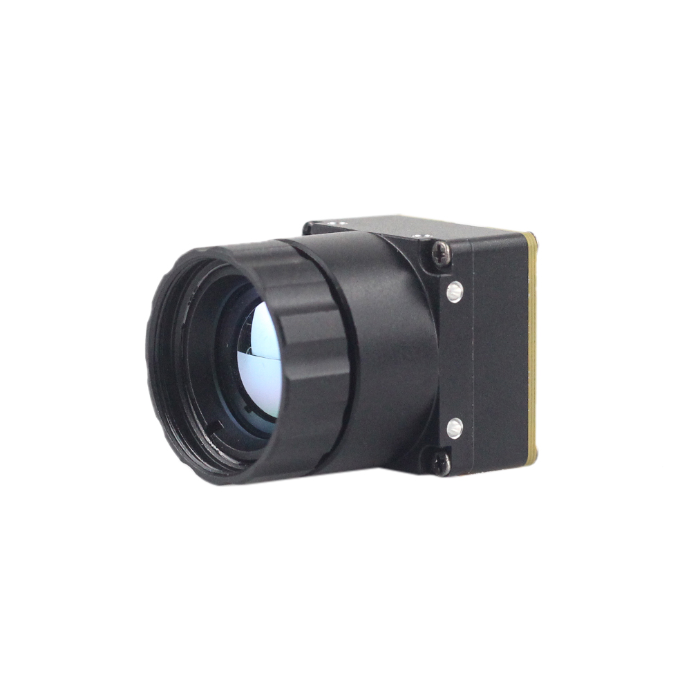
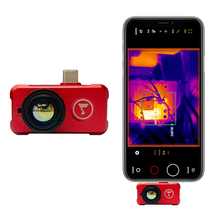
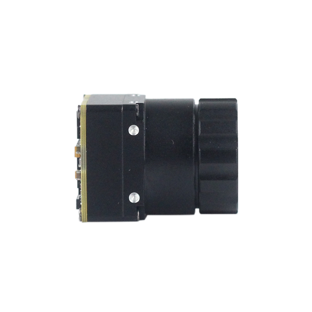
The Mini 256 Uncooled LWIR thermal Camera Module integrates high-sensitivity VOx microbolometers to provide clean thermal imagery and reliable radiometric readouts. Built on an architecture similar to payloads used on DJI airframes for detecting buried ordnance, this core is tailored for ultra-light aerial deployments where every gram counts. It maintains tight temperature accuracy across challenging, fluctuating outdoor flight profiles.
| Resolution | 256 × 192 pixels |
| Detector Type | Uncooled LWIR VOx Microbolometer |
| Radiometric Output | Full-scene uniform radiometry and temperature measurement |
| Primary Application | Sub-surface mine detection, micro-drones, agile robotic payloads |
Mini 640 Uncooled LWIR Thermal Camera Module
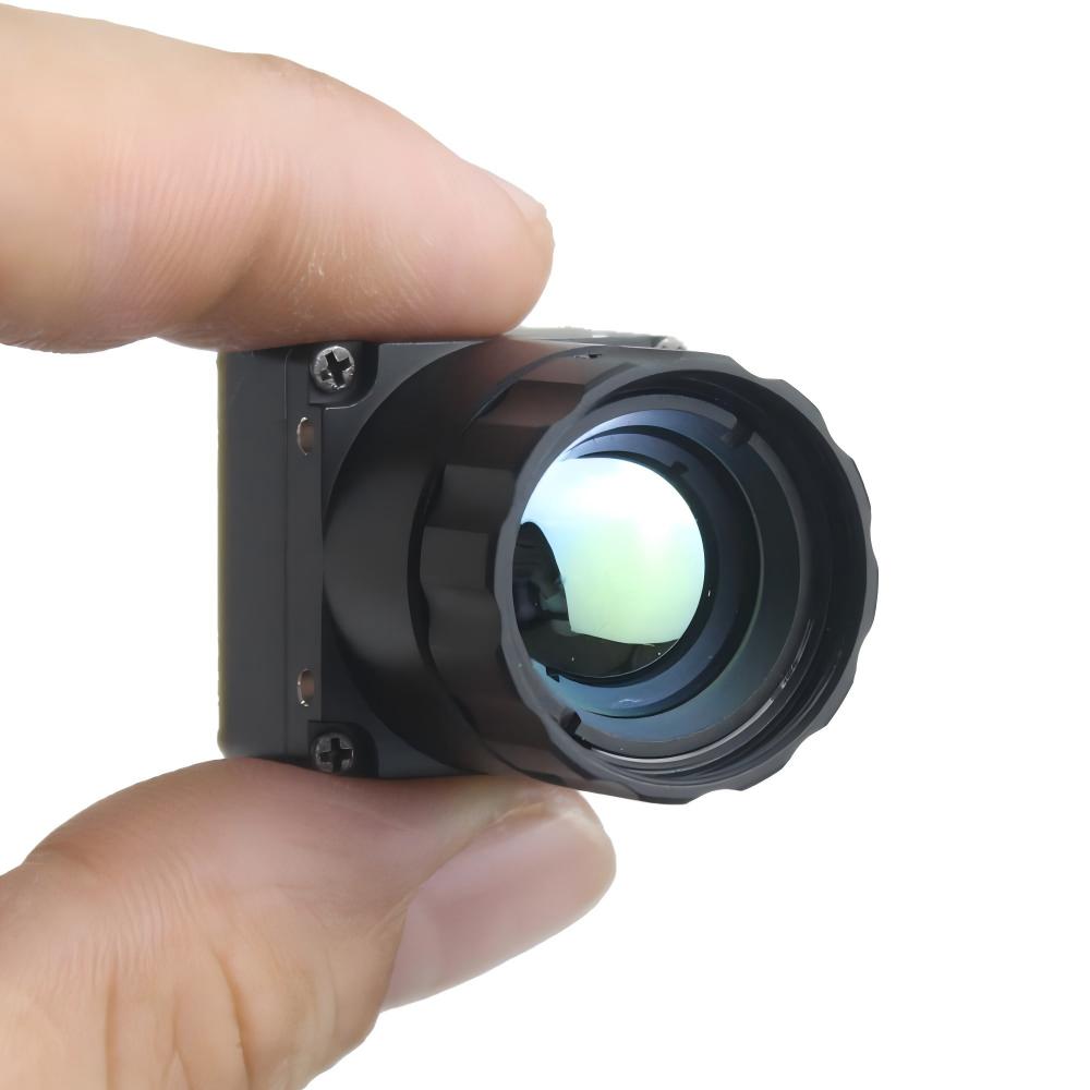
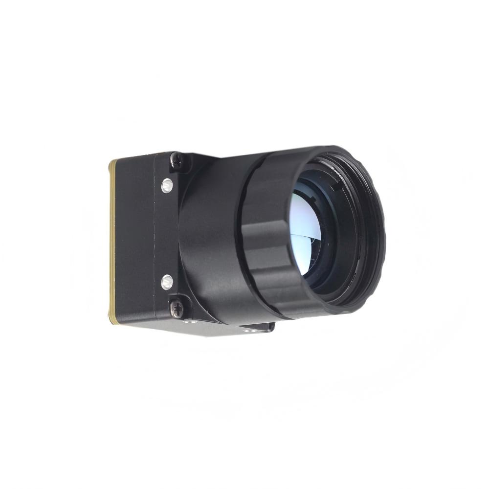
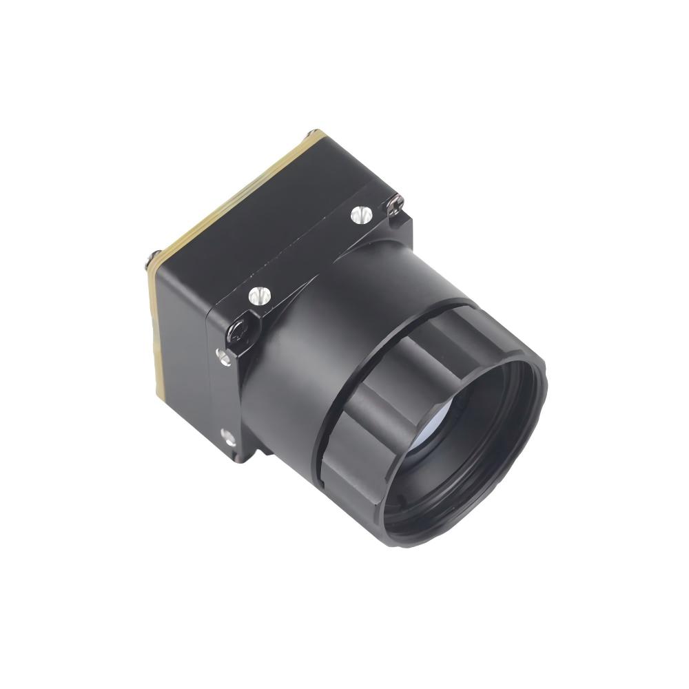
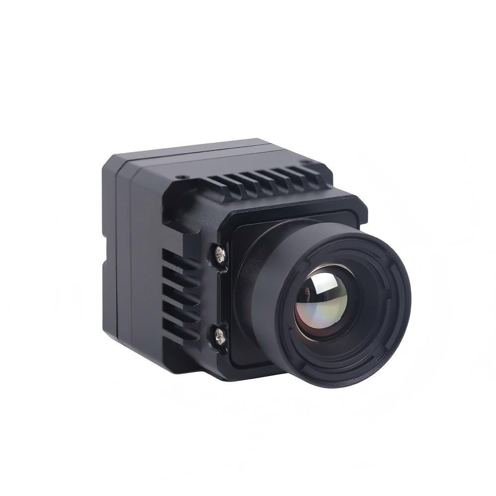
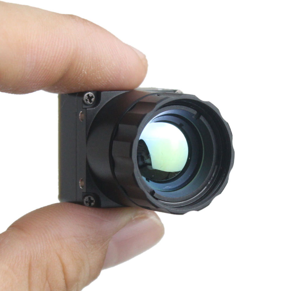
The Mini 640 uncooled infrared module delivers crisp image detail, miniature dimensions, and low unit costs. Measuring just 21mm × 21mm at the chassis, this core provides 640×480 resolution (with 640×512 optionality) and supports an expansive family of lenses: 5, 9, 13, 18, 35, 50, 75, 100, and 150mm. Built for stability across harsh field environments, it integrates cleanly into commercial and tactical airframes for long-range tracking, reconnaissance, and multi-sensor surveillance suites.
| Resolution | 640 × 480 / 640 × 512 optional |
| Footprint Dimensions | 21mm × 21mm (Micro-housing) |
| Supported Lenses | 5mm, 9mm, 13mm, 18mm, 35mm, 50mm, 75mm, 100mm, 150mm |
| Host Connectivity | USB (UVC-compliant), Digital Parallel, Serial Control |
| Primary Application | Tactical drones, long-range perimeter security, stabilized gimbals |
7. Comprehensive Technical FAQ
Why choose an ODM thermal imaging module over hobbyist sensors (like MLX90640) for drone mapping and scopes?
Industrial ODM modules utilize true 256×192 or 640×512 VOx microbolometer FPAs, delivering up to 327,680 individual pixels. With sensitivity figures running below 35mK–40mK and frame rates at a smooth 25Hz/50Hz/60Hz, these cores resolve fine soil density variances (for finding unexploded ordnance) or small structural defects from high-standoff flight corridors. They come backed with mature C/C++ driver SDKs, deterministic hardware triggering, and synchronized frame-by-frame radiometric metadata, ensuring orthomosaic mapping engines get georeferenced, blur-free data every single frame.
How does your thermal module ODM process address SWaP (Size, Weight, and Power) constraints?
On the power side, we maintain full-frame operational draw under 1.0W by deploying ultra-efficient low-power FPGAs and dedicated ASICs running bare-metal logic rather than power-hungry general-purpose processors. We also offer a wide selection of matched optics—from compact 5mm lenses up to 150mm telephoto assemblies—so you don't carry the weight of an oversized optical train. That allows our cores to balance smoothly inside compact multi-axis drone gimbals, weapon-mounted scopes, and sealed industrial nodes without draining the host battery.
What level of software and hardware customization is included in the ODM service?
On the optical and firmware front, we configure Germanium or Chalcogenide lenses with specialized AR or rugged DLC coatings. Our firmware engineers build application-specific ISP routines, including custom NUC look-up tables, tunable Digital Detail Enhancement (DDE), and adaptive histogram compression. We can also integrate lightweight Edge AI models directly into the module’s FPGA/ISP to flag humans, vehicles, or heat anomalies before video serialization, giving you a completely turnkey smart sensor package.
📚 References & Further Reading
- ⚙️ Industry Standard: OpenCV Open Source Computer Vision Library
- ⚙️ Industry Standard: Seeed Studio Edge Computing Ecosystems
- ⚙️ Related Guide: Video Performance Analysis of Uncooled LWIR 640 Thermal Camera Modules
- ⚙️ Related Guide: Engineering Guide to OEM Thermal Imaging Core Integration
- ⚙️ Related Guide: Multi-Functional Infrared Night Vision Optical Platform Specifications