
Thermal Module SDK for Integration: Developer Guide for Embedded AI & Radiometry
2026年9月7日
Wholesale Thermal Camera Module: High-Performance LWIR Sensor Cores for OEM & Drones
2026年9月9日
Custom Infrared Camera Core: High-Resolution OEM Thermal Imaging Solutions
Here's the deal with modern electro-optical systems engineering: the days of accepting compromises between razor-sharp optical sensitivity, brutal Size, Weight, and Power (SWaP) budgets, and real-time edge processing are over. Whether you are packaging a payload for an attritable uncrewed aerial system (UAS), building a forward-looking infrared (FLIR) handheld targeting sight, or standing up 24/7 predictive industrial arrays, you need an adaptable custom infrared camera core. It has to act as an open, modular building block—not some locked-down proprietary black box from an OEM vendor who refuses to hand over register-level control.
In the shop, we routinely watch standard off-the-shelf thermal engines choke real programs. They radiate heat straight back into their own detector arrays, pack oddball mounting patterns that wreck optomechanical balancing, force clunky proprietary video transport layers, and run bloated firmware that caps your frame rate, blows up pipeline latency, and cripples your onboard edge AI chips.
Solving these bottlenecks demands complete ground-up customizability across the entire signal and hardware chain. You have to tailor the uncooled long-wave infrared (LWIR) microbolometer detector array, engineer athermalized optical glass, specify low-noise Application-Specific Integrated Circuit (ASIC) readout electronics, and break out field-ready native interfaces like MIPI CSI-2, USB 3.0, and RJ45 RTSP streaming. This blueprint breaks down the exact physical, optomechanical, and electrical engineering requirements for specifying, building, and deploying mission-grade OEM thermal camera cores.
Table of Contents
- 👉 1. Physics & Architecture of Uncooled LWIR Microbolometers
- 👉 2. Engineering Trade-offs: SWaP-C Optimization in OEM Modules
- 👉 3. Hardware, Optics & Electrical Interface Customization
- 👉 4. Real-World OEM Product Comparison: High-Resolution vs. SWaP Cores
- 👉 5. Software Pipelines: Radiometric Calibration & Edge AI Integration
- 👉 6. Deep-Dive Integration FAQ
1. Physics & Architecture of Uncooled LWIR Microbolometers
At the center of any custom infrared camera core sits the Focal Plane Array (FPA). Look past the cryogenic Stirling coolers required by Mid-Wave Infrared (MWIR) or Short-Wave Infrared (SWIR) units operating near 77 Kelvin; modern Long-Wave Infrared (LWIR) OEM engines operate across the 8 µm to 14 µm atmospheric transmission window using uncooled thermal detectors. Target thermal flux strikes a microscopic suspended bridge membrane, exciting the material lattice and directly modulating the electrical resistance of an active thin-film layer.
How that tiny suspended bridge is built dictates your thermal sensitivity floor, raw signal-to-noise ratio (SNR), thermal time constant, and lifetime stability under heavy thermal shock.
Detector Materials: Vanadium Oxide (VOx) vs. Amorphous Silicon (a-Si)
When you spin up a custom thermal module design, the first fork in the road is selecting your active detector thin-film: Vanadium Oxide (VOx) or Amorphous Silicon (a-Si). Here is how they stack up on the test bench:
- ✅ Vanadium Oxide (VOx): VOx remains the unchallenged benchmark across defense, tactical, and high-accuracy industrial thermography. It delivers a solid Temperature Coefficient of Resistance (TCR) hovering between -2% and -3% per Kelvin at ambient operating temps. What really sets VOx apart is its remarkably low 1/f (flicker) electronic noise profile compared to silicon options. That low baseline noise lets custom cores reliably push Noise Equivalent Temperature Difference (NETD) thresholds below 35 mK to 40 mK using an f/1.0 aperture. When you are operating in washed-out, zero-contrast conditions—think thick maritime fog, heavy dust storms, or humid overcast skies—a low NETD is the sole reason you pull an actionable target signature instead of a screen full of gray mud.
- ⚙️ Amorphous Silicon (a-Si): Amorphous silicon runs through standard CMOS lithography fabs, depositing active detector layers directly on top of readout wafers. That keeps high-volume bill-of-materials (BOM) costs low for consumer gadgets. But you pay for it in performance: a-Si exhibits structural atomic disorder, which elevates internal 1/f noise floors and pins the TCR down near -1.5% to -2.0% per Kelvin. Most a-Si sensors hover with an NETD between 50 mK and 70 mK. Unless an extreme commercial cost target forces your hand, experienced electro-optical teams pick VOx every single time for mission-critical builds.
Pixel Pitch Evolution: The Shift to 12 µm and Optical Scaling
Thermal foundries have driven pixel pitch down from legacy 25 µm and 17 µm nodes straight to 12 µm microbolometer pixel pitches, with bleeding-edge R&D now refining 10 µm and 8 µm lithography. For an optomechanical design team, shrinking that pitch reshapes the entire physical architecture.
Pixel pitch directly dictates the active silicon footprint of the Focal Plane Array at any specified resolution. Take a classic 640×512 resolution engine: built on a 17 µm process, the sensor diagonal sits at 13.93 mm (an active area of 10.88 mm × 8.60 mm). Shift that exact same 640×512 array down to a 12 µm process, and the active area shrinks to 7.68 mm × 6.14 mm (diagonal: 9.83 mm). That is an active area reduction of more than 50%. The downstream engineering wins are massive:
- ✅ Compact, Lightweight Optics: To deliver the exact same Instantaneous Field of View (IFOV) and target spot size, a 12 µm core needs a focal length 29.4% shorter than a 17 µm array. Shorter focal lengths immediately drop the optical clear aperture required to preserve an f/1.0 light bucket. That eliminates substantial mass and volume of single-crystal optical Germanium, which is both dense and expensive.
- ✅ Quadrupled Spatial Information Density: If you have an existing payload bay built around a 17 µm 640×512 engine, you can swap in a native 1280×1024 (SXGA) 12 µm custom infrared camera core within that exact physical optical envelope. You jump from 327,680 pixels to 1,310,720 pixels. That quadruples your on-target pixels, dramatically extending Detection, Recognition, and Identification (DRI) standoffs under Johnson's criteria without adding a gram of weight to your platform.
Sensor Packaging: Wafer-Level Packaging (WLP) vs. Ceramic Metal-Can
Microbolometer bridges cannot function in open air; atmospheric molecules create parasitic thermal conduction that completely bleeds away incoming photon energy. To work, the detector bridge must sit in a sealed, hard vacuum ($<10^{-3}\text{ Torr}$). For decades, manufacturers achieved this by packaging detectors inside massive ceramic or metal-can vacuum jackets, sealing them with sapphire or germanium windows and activated non-evaporable getters (NEG).
Today's compact camera cores rely on Wafer-Level Packaging (WLP). A cap wafer made of etched silicon or germanium—complete with micromachined internal cavities and antireflective coatings—is aligned and hermetically bonded directly to the microbolometer detector wafer under hard vacuum before the wafer is ever diced. WLP shrinks the z-height of the sensor footprint by up to 70%, sheds chassis mass down to grams, and boosts mechanical survivability against shock loads exceeding 1,500g at 0.4 ms pulses. To bring these multi-gigabit differential sensor lines down to the processing boards without picking up stray RF from switching power supplies, we rely on high-density micro-pitch interconnect systems from proven suppliers like TE Connectivity to protect analog signal purity.
2. Engineering Trade-offs: SWaP-C Optimization in OEM Modules
Every embedded electro-optical build boils down to managing Size, Weight, Power, and Cost (SWaP-C). When engineering a custom infrared camera core into an airframe, ground vehicle, or handheld device, you are constantly balancing thermal dissipation, electrical draw, and processing overhead.
ASIC vs. FPGA Image Signal Processing (ISP) Architectures
The processing engine behind the FPA handles heavy digital heavy lifting: Two-Point Non-Uniformity Correction (NUC), Bad Pixel Replacement (BPR), Dynamic Range Compression (DRC), and Digital Detail Enhancement (DDE). Historically, custom thermal modules leaned hard on Field Programmable Gate Arrays (FPGAs) like Xilinx Artix or Zynq chips. FPGAs give you reconfigurable logic, but they carry distinct penalties in tight payloads:
- ⚙️ Excess Power and Thermal Runaway: High-gate-count FPGAs running multi-clock ISP pipelines chew through 3.0 W to 8.0 W of continuous power. Trap that inside a sealed IP67 gimbal or an enclosed handheld scope, and you generate localized thermal plumes that heat the detector array unevenly.
- ⚙️ Board Real Estate and Boot Latency: FPGAs require supporting infrastructure: multiple low-dropout regulators (LDOs), dedicated power sequencers, SPI flash boot memory, and high-speed DDR RAM. That easily balloons the core into a thick three-board stack that requires seconds to boot up.
Modern custom infrared cores cut this bulk by using dedicated Application-Specific Integrated Circuits (ASICs). Hardwiring the spatial filters, non-uniformity math, and frame-formatting logic directly into custom low-power silicon cuts core power draw below 1.2 Watts at full 50Hz/60Hz frame rates. The ASIC ISP also eliminates external frame-buffer holding cycles, keeping glass-to-wire pipeline latency down to sub-frame numbers ($<30\text{ ms}$). That sub-30ms performance is the baseline requirement for closed-loop counter-unmanned aerial systems (C-UAS) tracking gimbals and tight missile-defense stabilization loops.
Internal Thermal Dissipation & Drift Compensation
An uncooled microbolometer detects tiny fractions of a degree. It cannot tell the difference between infrared photons arriving through the lens and stray heat radiating off a hot switching inductor or an edge processor sitting half an inch away. If internal heat bleeds into the FPA unevenly, your image develops heavy spatial vignetting, nasty fixed-pattern noise (FPN), and drifting radiometric temperature readings.
Taming internal thermal coupling requires solid board-level discipline:
- ⚙️ Isolate the Sensor Substrate: Mechanically and thermally decouple the FPA board from the main digital processing engine using engineered low-conductivity PEEK standoffs or routed isolation cutouts in the FR4 board stack.
- ⚙️ Design Dedicated Heat Paths: Drop thick continuous 2 oz or 3 oz copper ground planes into your PCB, stitch thermal via arrays beneath heat-generating components, and drop high-performance thermal gap pads ($>6\text{ W/m}\cdot\text{K}$) directly between the power stage and the external housing. The heat needs to sink into the outer chassis, completely avoiding the lens mount and optical barrel.
- ⚙️ Thermistor Multiplexing: High-end custom engines place calibrated NTC thermistors across the housing: right at the optical lens collar, on the interface board, and directly behind the bolometer die. The internal firmware continuously reads this thermal mesh, dynamically adjusting spatial mathematical offset compensation tables in real time. That keeps the image uniform without constantly firing an intrusive mechanical shutter.
3. Hardware, Optics & Electrical Interface Customization
A truly usable custom infrared core must adapt to its environment. The mechanical lens mount and electrical pinouts are the physical bridge between raw thermal physics and your software stack.
Optical Materials: Monocrystalline Germanium vs. Chalcogenide Glass
Standard optical glasses like BK7 or fused silica are completely opaque across the 8 µm to 14 µm band. To build an LWIR optical assembly, you rely on two core optical media:
- ⚙️ Monocrystalline Germanium (Ge): Germanium remains the gold standard for high-performance thermal optics. It delivers an exceptionally high refractive index ($n \approx 4.0$ at 10 µm) combined with remarkably low chromatic dispersion. This high index lets optical engineers design compact, fast lenses ($f/1.0$ to $f/1.2$) using just two or three elements while keeping spherical aberrations well controlled. However, Germanium has a massive thermal focal drift coefficient ($dn/dt \approx 3.96 \times 10^{-4}\text{ K}^{-1}$), meaning uncompensated lenses quickly lose focus as ambient temperatures shift. Germanium also suffers from thermal runaway, going nearly opaque to LWIR energy once its temperature crosses 100°C.
- ⚙️ Chalcogenide Glass (e.g., GASIR, AMTIR): Chalcogenide glasses are amorphous alloys formed from sulfur, selenium, and tellurium. They feature substantially lower $dn/dt$ values than Germanium, making them ideal for passive optical athermalization. By pairing single-point diamond turned (SPDT) Germanium elements with precision molded Chalcogenide elements inside a balanced aluminum or invar barrel, your lens stack holds diffraction-limited focus across wide operating environments (-40°C to +80°C) without the weight, complexity, and power draw of a motorized focus drive.
Electrical Data Transport & Protocol Interfacing
Every payload presents its own wiring and interface challenges. A modular custom infrared core should offer native, solderable, or pin-compatible interfaces to suit the host platform:
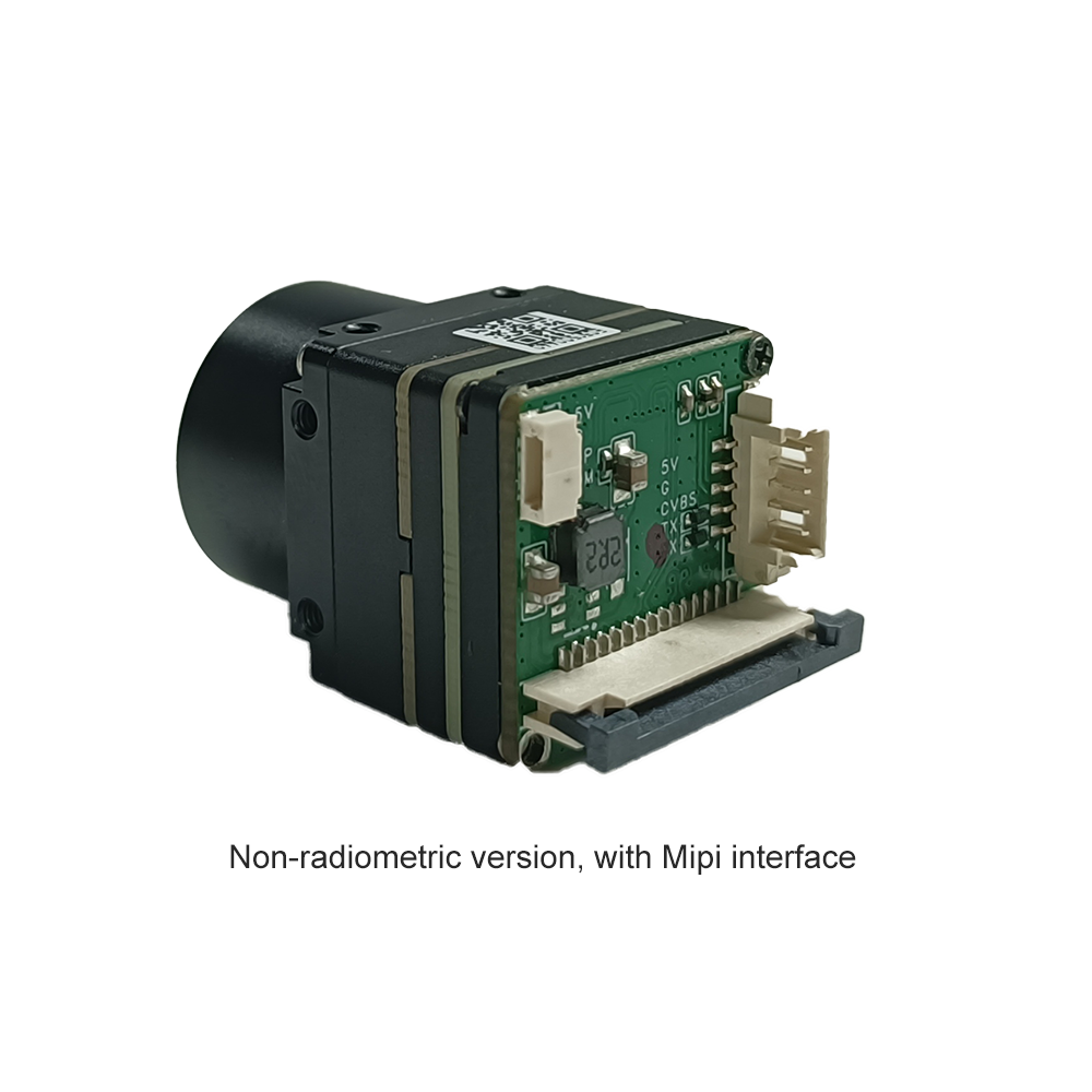
- ✅ MIPI CSI-2: The modern standard for direct interconnects to System-on-Chips (SoCs) like the NVIDIA Jetson Orin family, NXP i.MX8, or Rockchip RK3588. MIPI CSI-2 bypasses protocol-conversion hardware, pushing raw 14-bit or 16-bit thermal pixel streams over low-voltage differential pairs directly into the host processor's hardware Image Signal Processor or unified memory pool.
- ✅ USB 3.0 (UVC Compliant): The go-to interface for bench test benches, industrial automated optical inspection (AOI), and PC-based systems. Operating on native UVC drivers across Linux, Windows, and macOS, a UVC core streams raw 16-bit greyscale radiometric data or 8-bit colorized frames right out of the box, while exposing a simple virtual COM port for core register configuration.
- ✅ RJ45 Ethernet IP (RTSP / ONVIF): Built for fixed facility infrastructure, process monitoring, and perimeter security. An onboard network chip handles H.264 or H.265 compression, feeding an RTSP stream formatted to ONVIF Profile S and T standards directly into your Video Management System (VMS) without extra intermediary hardware.
- ✅ CVBS Analog (NTSC/PAL): Even with modern digital networks, direct analog composite video remains unmatched for ultra-low latency analog FPV downlinks on attritable drones and tactical helmet displays. To see how these modules perform in the air under dynamic vibration, review our field footage from this video of thermal imaging camera module with drone flight trials.
4. Real-World OEM Product Comparison: High-Resolution vs. SWaP Cores
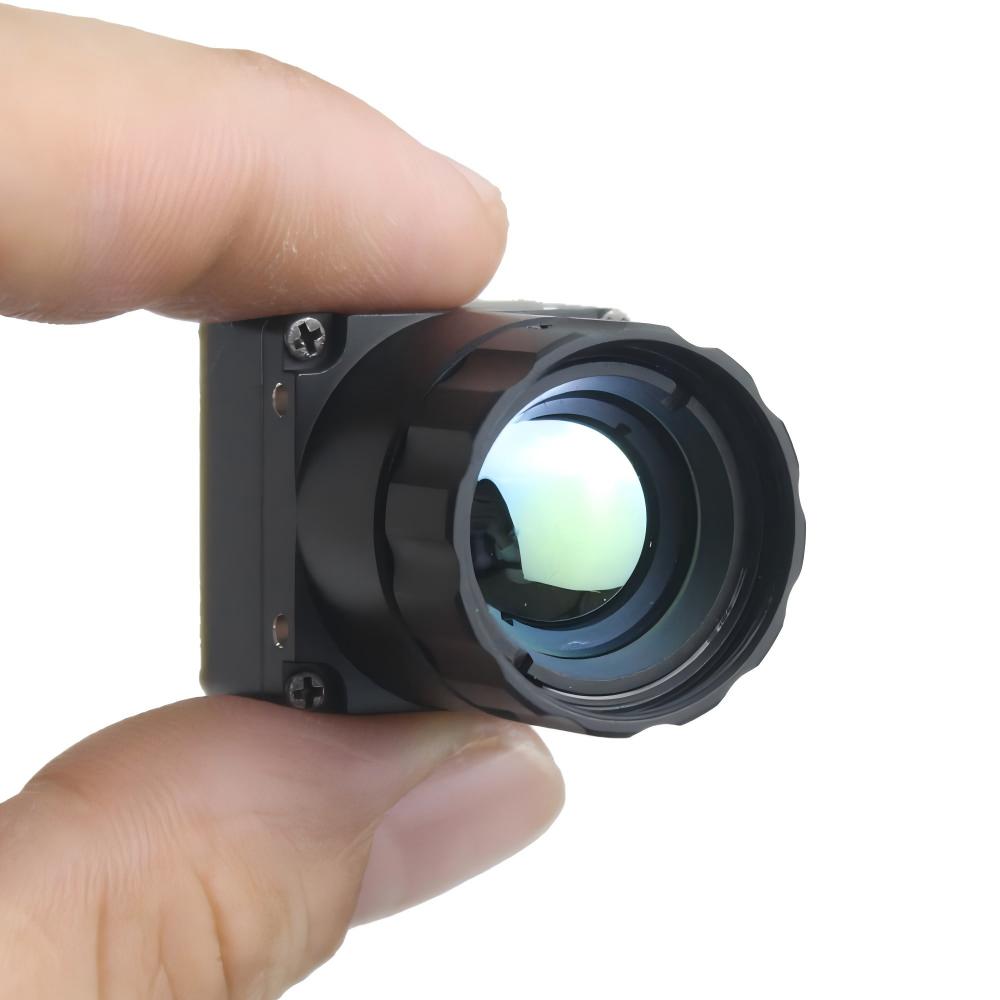
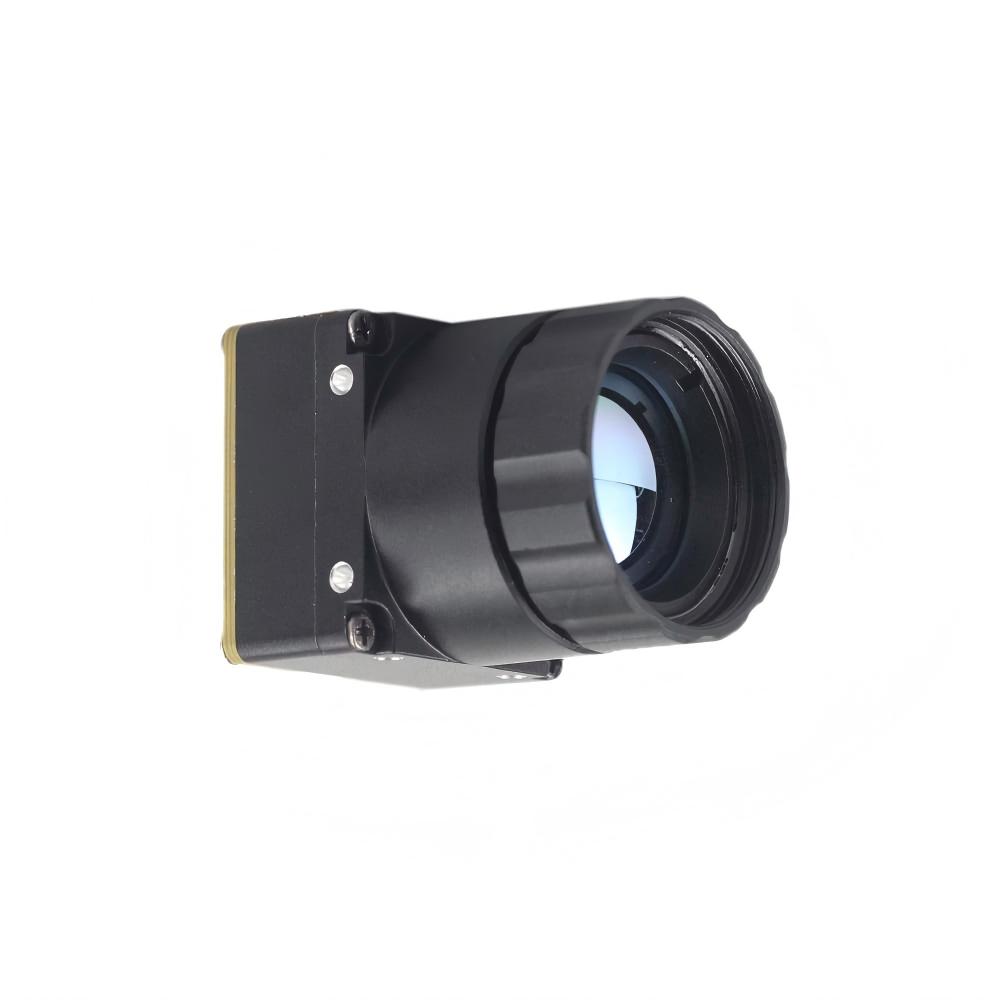
To see how these architectural choices play out on real flight hardware, let's look at two production-ready cores designed for distinct mission envelopes: the long-range High Resolution Uncooled Infrared 1280*1024 Thermal Imaging LWIR Camera and the tight-envelope Uncooled Infrared RJ45 CVBS RTSP IP 640*512 Thermal Sensor Camera Module.
Platform A: High Resolution Uncooled Infrared 1280*1024 Thermal Imaging LWIR Camera
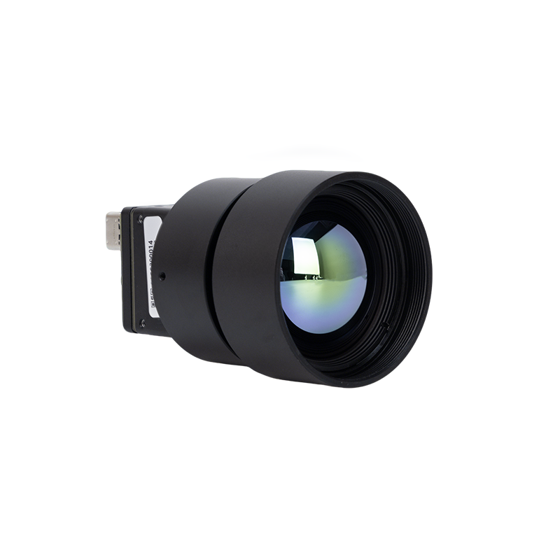
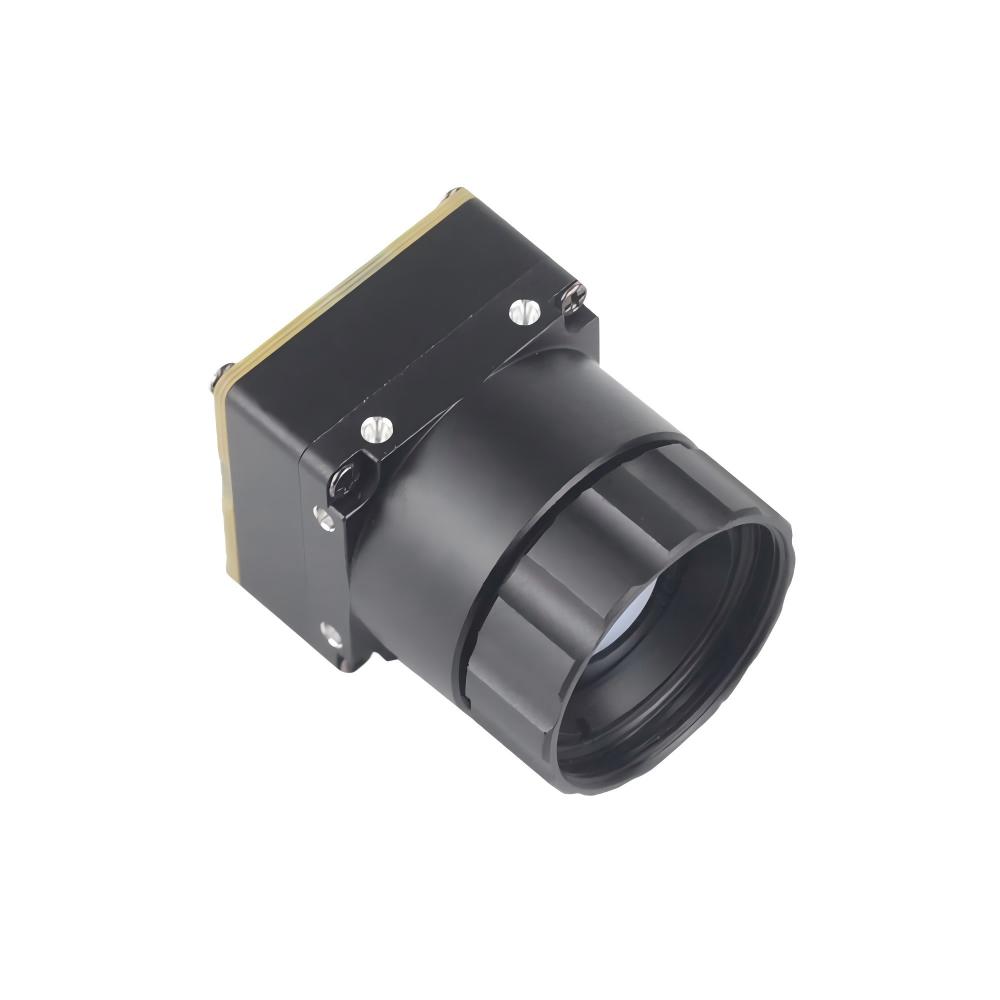
The 1280×1024 custom infrared camera core is engineered for mission-critical electro-optical applications where spatial target resolution, instantaneous field of view, and extreme standoff distance are paramount. Fabricated with a high-sensitivity uncooled Vanadium Oxide (VOx) focal plane array, this core packs 1.31 million detector pixels on a tight 12 µm pitch, achieving an industry-leading NETD sensitivity of <35 mK. The native SXGA resolution provides four times the pixel density of standard 640×512 VGA thermal modules, allowing operators to detect, recognize, and track human and vehicular targets at multi-kilometer distances without requiring excessive optical magnification.
Optically, the module comes standard with a factory-calibrated 25 mm athermalized high-transmission Germanium lens, maintaining absolute focus integrity across the entire industrial temperature envelope. The optomechanical interface supports customized optical configurations, including 19 mm, 35 mm, 50 mm fixed optics, and motorized continuous zoom groups. The digital core supports dual-output pipelines: high-speed digital streaming via USB Type-C and raw parallel CMOS/MIPI CSI-2, alongside serial control via RS-232/RS-422 and UART. Full-frame radiometric output enables pixel-by-pixel temperature extraction, making it an ideal core for border surveillance arrays, counter-UAS tracking pedestals, and automated predictive substation monitoring.
Platform B: Uncooled Infrared RJ45 CVBS RTSP IP 640*512 Thermal Sensor Camera Module
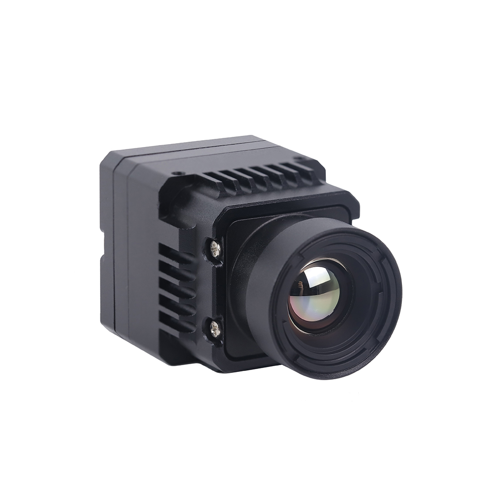
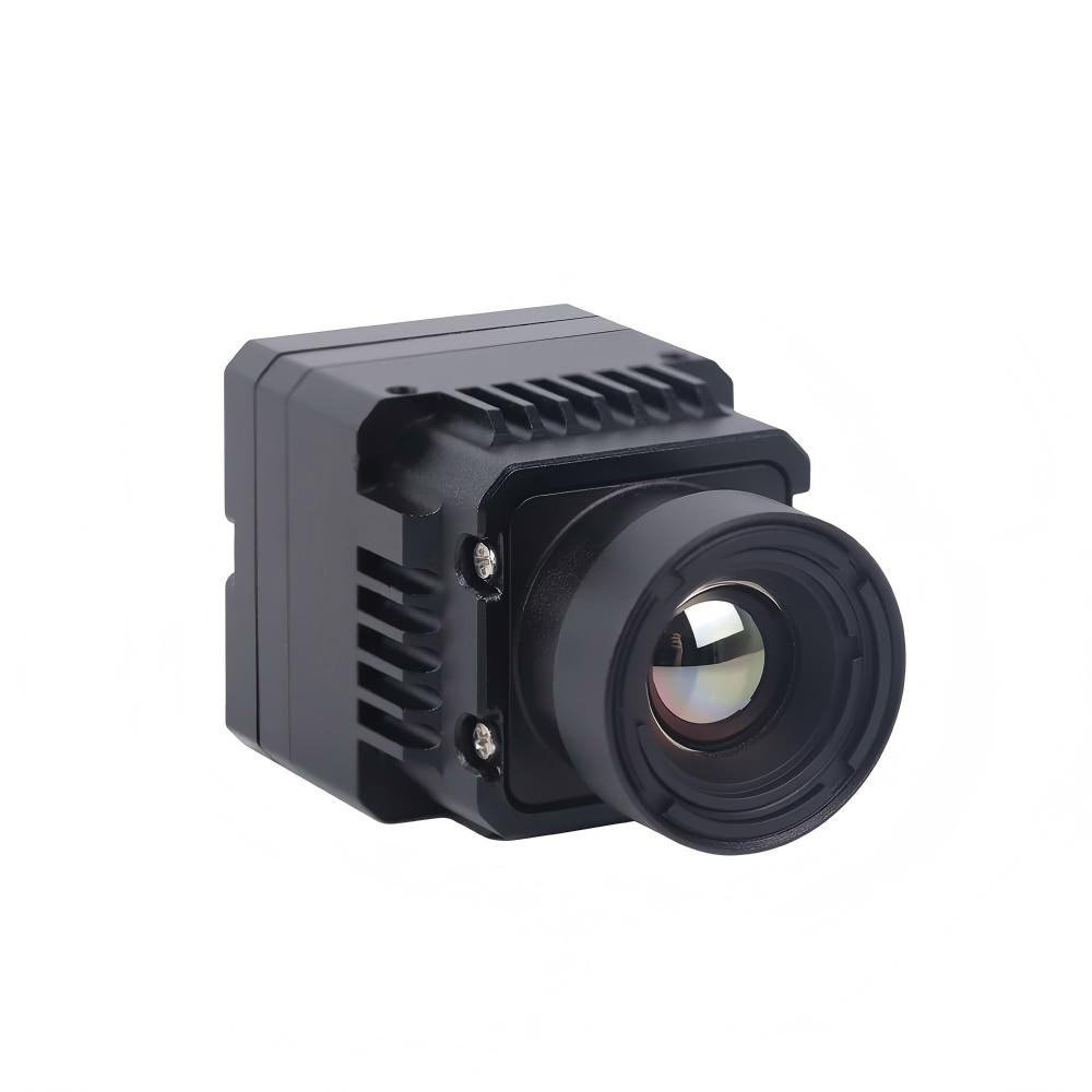
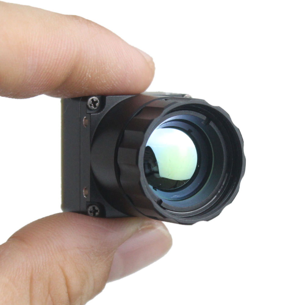
Designed specifically to meet stringent SWaP parameters in uncrewed aerial vehicles, miniature robotic platforms, and compact surveillance systems, this 640×512 thermal core is driven by a specialized low-power imaging ASIC engine. Built around a 12 µm VOx microbolometer array operating at <40 mK NETD, this module prioritizes integration flexibility by natively incorporating both an analog CVBS interface and a complete hardware-encoded RJ45 IP network stack on a miniature electronics footprint. Total core power consumption is throttled to less than 1.2 Watts, preventing parasitic heat buildup in tightly enclosed drone gimbals.
The module encodes real-time H.264/H.265 RTSP video streams natively, allowing system designers to connect the core directly into network switches, wireless IP data links, or standard Ethernet routers without requiring external SBC encoding hardware. Concurrently, the analog CVBS port feeds direct, uncompressed video signals to legacy drone FPV transmitters with sub-frame transmission latency. With customizable optical mounts accommodating ultra-compact 9.1 mm, 13 mm, and 19 mm athermalized lenses, this module provides the definitive hardware blueprint for tactical micro-gimbals and autonomous mobile robot (AMR) obstacle-avoidance suites.
Here is an apples-to-apples technical matrix comparing these platforms across baseline integration metrics:
| Specification Parameter | High-Resolution Core (1280×1024) | SWaP-Optimized Core (640×512) |
|---|---|---|
| Detector Type & Material | Uncooled VOx Microbolometer FPA | Uncooled VOx Microbolometer FPA |
| Array Resolution | 1280 × 1024 pixels (SXGA) | 640 × 512 pixels (VGA) |
| Pixel Pitch | 12 µm | 12 µm |
| Spectral Band | 8 µm to 14 µm (LWIR) | 8 µm to 14 µm (LWIR) |
| Thermal Sensitivity (NETD) | < 35 mK (@ f/1.0, 300K) | < 40 mK (@ f/1.0, 300K) |
| Frame Rates Supported | 25 Hz / 30 Hz / 50 Hz | 25 Hz / 30 Hz / 50 Hz / 60 Hz |
| Power Consumption | Approx. 2.0 W – 2.8 W (Config Dependent) | < 1.2 W (Ultra-Low Power ASIC) |
| Hardware Video Interfaces | USB Type-C, Raw 16-bit CMOS, MIPI CSI-2 | RJ45 Ethernet (IP RTSP), Analog CVBS |
| Optical Configurations | 25 mm Athermalized (Options: 19/35/50 mm, CZ) | Fixed Focus: 9.1 mm, 13 mm, 19 mm |
| Primary Target Use-Case | C-UAS, Long-Range Defense, Fixed Radiometry | UAV Micro-Gimbals, Tactical Scopes, AMRs |
5. Software Pipelines: Radiometric Calibration & Edge AI Integration
Capturing raw infrared energy on the microbolometer bridge is only the first step. You have to turn those microvolt resistance changes into stable digital data that an edge computer or targeting algorithm can parse without human intervention.
Raw Digital Numbers (DN) vs. Radiometric Temperature Linear (T-Linear)
When pulling raw data out of your custom core, you generally run one of two operational modes depending on whether your software cares about quantitative surface thermography or dynamic situational vision:
- ⚙️ Raw Digital Numbers (DN Mode): In this mode, the core bypasses radiometric conversion and pumps out uncalibrated 14-bit or 16-bit counts directly from the ADC post-NUC. These Digital Numbers represent relative thermal contrast across the scene. They do not account for external atmosphere, optics transmissivity, or housing drift. If your system runs automated computer vision pipelines—like training a neural network to detect humans, vehicles, or airborne drones—DN mode is the correct choice. You skip radiometric processing overhead and slash end-to-end latency.
- ⚙️ Temperature-Linear (T-Linear Mode): If you are monitoring substation transformers, detecting industrial pipeline leaks, or managing structural firefighting ops, relative intensity is useless; you need calibrated temperatures per pixel. In T-Linear mode, the onboard ASIC uses multi-point factory blackbody calibration tables to convert raw readings directly into absolute temperature values. The stream delivers a linear output where each LSB maps directly to temperature (for instance, 0.1 K or 0.01 K per count). For specialized environments, our industrial thermal camera selection guide walks through dynamic range scaling from -20°C up past 1200°C.
Non-Uniformity Correction: Mechanical Shutter vs. Shutterless Algorithms
Every single bolometer pixel on that micro-machined array has a slightly different baseline resistance and thermal response curve. Without real-time corrections, fixed-pattern noise (FPN) rapidly blinds your image behind an impenetrable curtain of static.
You have two practical approaches to address this drift:
- ⚙️ Mechanical Shutter NUC: A solenoid drops an insulated paddle in front of the array for 200 ms to 400 ms. The core samples that uniform surface, computes offset corrections across the pixel field, and updates its active correction table. It is rock-solid and straightforward, but that physical shutter has moving parts that can fail under shock, makes an audible click, and freezes your video feed. In a terminal missile-guidance track or a high-speed drone dive, a 300 ms video blackout is completely unacceptable.
- ✅ Shutterless Scene-Based NUC (SBNUC): For high-reliability, zero-freeze architectures, we rely on Scene-Based NUC. The DSP continuously evaluates frame-to-frame pixel statistics and platform motion vectors. By mathematically isolating fixed spatial noise from moving scene dynamics over time, the algorithm updates correction offsets without moving mechanical parts. Zero freeze, zero mechanical click, and zero moving parts to wear out. For an in-depth breakdown of SBNUC implementation parameters, consult the thermal module integration guide.
Embedded Edge AI Pipelines (NVIDIA Jetson & Embedded Linux)
Most modern custom cores bypass display panels altogether, routing thermal frames straight into edge neural networks. Bringing high-bandwidth 16-bit thermal video into an NVIDIA Jetson Orin Nano, AGX Orin, or modern embedded Linux platform requires a clean memory strategy.
Look at the memory pipeline: you cannot afford to have your host CPU copying multi-megapixel 16-bit frames around system RAM. We write custom Video4Linux2 (V4L2) driver layers that set up direct DMA ring buffers. When raw thermal frames arrive over MIPI CSI-2 or USB3, DMA routes them straight into unified CUDA or NPU memory using hardware-accelerated memory APIs like NVIDIA's NvBuffer. This zero-copy path completely bypasses CPU memory bottlenecks, freeing hardware accelerators to run heavy edge networks—like YOLOv8-Thermal, MobileNet-SSD, or custom infrared segmentation models—at over 50 frames per second with minimal CPU load.
6. Deep-Dive Integration FAQ
How do I integrate a custom infrared camera core with single-board computers like Raspberry Pi or NVIDIA Jetson for low-latency streaming?
Can a custom thermal camera core be tailored for SWaP-constrained applications like drones and handheld scopes?
What level of customization is supported for OEM/ODM thermal imaging modules?
📚 References & Further Reading
- Industry Standard: High-reliability interconnect systems and electromechanical board interfaces from TE Connectivity
- Related Guide: Comprehensive selection parameters for machine vision in our industrial thermal camera selection guide
- Related Guide: Step-by-step firmware and hardware integration protocols detailed in the thermal module integration guide
- Field Demonstration: Real-world flight payload verification shown in the video of thermal imaging camera module with drone