
High-Resolution IR Thermal Camera Modules: Complete Industrial OEM Buying Guide
2026年10月22日
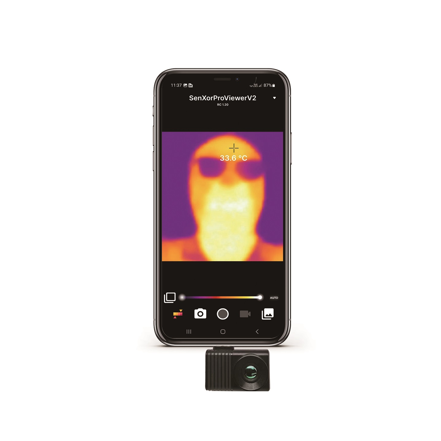
Thermal Camera for Android: Pro Smartphone Attachments vs. Standalone Modules Guide
2026年10月23日
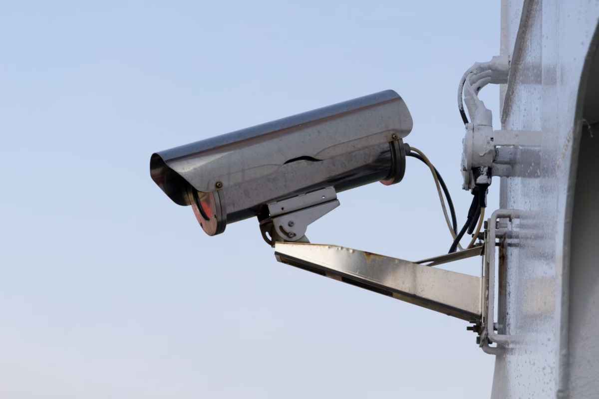
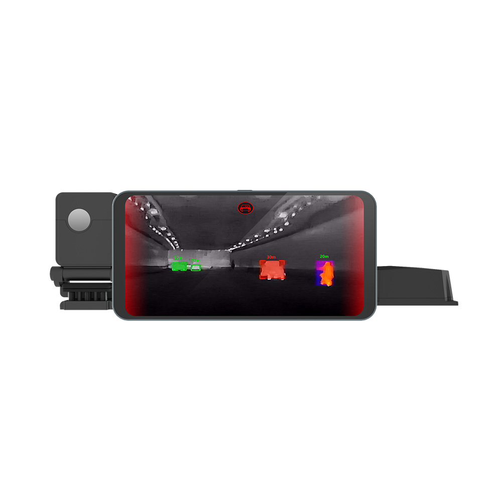
Infrared Thermal Imaging Camera Guide: Real Resolution, Sensor Tech & Buying Truths
In modern optical engineering, few components are as routinely obfuscated by marketing hyperbole as the infrared thermal imaging camera. Industrial procurement teams and systems integrators are frequently bombarded with consumer-tier specifications that boast "high-definition thermal output," only to discover upon benchtop characterization that the underlying sensor core relies on an aggressively upscaled 80×60 or 160×120 microbolometer array masked by spatial smoothing filters. In mission-critical environments—such as high-voltage switchgear inspection, automated PCB thermal profiling, long-range perimeter defense, and drone-mounted tactical surveillance—these interpolated artifacts do not merely degrade visual fidelity; they conceal micro-thermal deltas, introduce catastrophic radiometric error, and trigger false positives in automated computer vision pipelines.
Achieving true situational awareness and quantitative thermography requires stripping away marketing claims to evaluate the fundamental optomechanical and semiconductor architecture of the thermal core. An uncooled Long-Wave Infrared (LWIR) sensing engine must be assessed on the physical properties of its Vanadium Oxide (VOx) focal plane array, its true native pixel pitch (down to 12µm), the vacuum packaging integrity of the sensor die, and the optical transmission characteristics of its monocrystalline Germanium optics. Understanding the mechanical realities of Noise Equivalent Temperature Difference (NETD), native versus mathematically synthesized spatial resolution, and low-latency embedded interface buses like MIPI CSI-2 is the only path to engineering a system that delivers absolute radiometric repeatability across harsh airborne and terrestrial deployments.
Table of Contents
- 👉 1. Photons vs. Heat: The Fundamental Physics of LWIR Thermal Sensing
- 👉 2. The Resolution Reality: Native Sensor FPA vs. Software Interpolation
- 👉 3. Critical Hardware Metrics: NETD, Frame Rates, and Germanium Optics
- 👉 4. Embedded Integration: MIPI CSI-2, USB, and Edge-AI Platforms
- 👉 5. Industrial & OEM Hardware Specification Showcase
- 👉 6. OEM Thermal Core Selection Matrix
- 👉 7. Deep-Dive Technical FAQ
1. Photons vs. Heat: The Fundamental Physics of LWIR Thermal Sensing
An industrial infrared thermal imaging camera does not register photons within the visible spectrum (0.38 to 0.75 µm) or the near-infrared band (NIR, 0.75 to 1.4 µm). Instead, it functions as a specialized, uncooled radiometric sensor array that detects radiant flux across the Long-Wave Infrared (LWIR) atmospheric transmission spectrum, precisely between 8.0 and 14.0 µm. Every physical body with a temperature above absolute zero (0 Kelvin or −273.15°C) emits continuous electromagnetic radiation governed by Planck's Radiation Law, which describes the spectral radiance of an ideal blackbody as a function of temperature and wavelength:
By integrating Planck's law across all operational wavelengths, we obtain the Stefan-Boltzmann Law, which states that total radiant exitance is proportional to the fourth power of thermodynamic temperature multiplied by surface emissivity: W = εσT&sup4;. Because terrestrial objects and industrial components generally sit between −40°C and +500°C, their peak spectral emission falls precisely inside the 8 to 14 µm band according to Wien's Displacement Law (λ_max × T ≈ 2898 µm·K). At ambient room temperature (300 K), the peak emission occurs at approximately 9.66 µm.
To capture this passive radiant exitance without cryogenic cooling, the core of an uncooled thermal camera uses a Focal Plane Array (FPA) populated by thousands of microscopic thermal detector cells known as microbolometers. Each individual microbolometer pixel consists of an ultra-thin absorbing membrane suspended over a silicon Readout Integrated Circuit (ROIC) by tiny mechanical support legs. These legs serve a dual function: they provide an electrical pathway for reading variations in resistance and establish a controlled thermal resistance path. The entire detector array is sealed within an ultra-high vacuum package to eliminate thermal convective loss to the surrounding air.
When incident LWIR radiation passes through specialized transmissive optics, it strikes the absorbing membrane. The absorbed thermal energy increases the membrane's physical temperature by a minute fraction of a degree. This temperature rise alters the electrical resistance of the active material. The ROIC sequentially injects a small bias current or voltage across the microbolometer matrix, measures the resistance delta across each pixel, and converts this analog shift into a high-precision digital output count (typically 14-bit or 16-bit raw data). System designers frequently experiment with initial resistance bridges and low-frequency telemetry using open-source hardware such as Arduino, or scale up to advanced embedded interface breakout bridges provided by Waveshare when prototyping high-speed embedded display adapters.
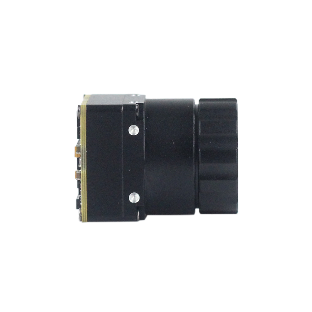
Engineers evaluating sensor hardware often wonder why standard CMOS image sensors cannot be modified with an optical filter to register thermal radiation. Our technical analysis on whether we can transform a standard camera into an infrared imaging device outlines the bandgap physics that prevent silicon from detecting wavelengths beyond 1.1 µm, explaining why uncooled microbolometers are mandatory for true thermal sensing.
1.1 Vanadium Oxide (VOx) vs. Amorphous Silicon (a-Si) Microbolometers
When selecting an uncooled thermal imaging engine, the microbolometer material is the primary architectural differentiator. Two materials dominate the industry:
- ⚙️ Vanadium Oxide (VOx): VOx is the industrial and military benchmark. It possesses an exceptionally high Temperature Coefficient of Resistance (TCR), typically ranging from −2% to −3% per Kelvin at room temperature, combined with exceptionally low electrical 1/f (flicker) noise. Because VOx films change resistance dramatically for even slight thermal shifts, sensors built with this material deliver outstanding thermal sensitivity (low NETD ≤ 30mK to 40mK). Furthermore, VOx membranes can be fabricated with significantly lower thermal mass, enabling fast thermal time constants (τ ≈ 8 to 12 ms). This rapid thermal dissipation eliminates motion smear, double edges, and ghosting in high-vibration airborne UAV gimbals and high-speed industrial pick-and-place automation.
- ⚙️ Amorphous Silicon (a-Si): Amorphous silicon was developed primarily as a high-volume, lower-cost alternative that could leverage standard commercial silicon foundry fabrication lines. While a-Si simplifies manufacturing logistics, it exhibits a noticeably inferior TCR (typically −1.5% to −2.5% per Kelvin) and suffers from pronounced internal 1/f electrical flicker noise. To achieve acceptable signal-to-noise ratios, a-Si pixels must be fabricated with larger physical volumes or subjected to aggressive temporal rolling-average frame filters. This inevitably increases the thermal time constant (τ ≈ 14 to 20 ms), inducing perceptible latency and severe spatial blurring during rapid target slewing or high-dynamic-range tracking.
1.2 Spectral Partitioning: Why 8–14 µm Dominates Industrial Imaging
The terrestrial atmosphere is far from transparent across the infrared spectrum. Diatomic and triatomic molecules—predominantly water vapor (H2O), carbon dioxide (CO2), and ozone (O3)—create massive optical absorption bands that completely extinguish thermal transmission over short distances. The practical infrared spectrum is thus strictly partitioned into distinct operational windows:
- ⚙️ Short-Wave Infrared (SWIR, 1.4 to 3.0 µm): Dominated by reflected photon flux rather than passive thermal emission. SWIR requires active illumination or high-temperature emitters (>500°C) and is typically captured using Indium Gallium Arsenide (InGaAs) photodiode arrays to penetrate glass envelopes, inspect silicon ingots, or see through maritime maritime haze.
- ⚙️ Mid-Wave Infrared (MWIR, 3.0 to 5.0 µm): An atmospheric transmission window where high-temperature thermal targets (such as jet turbine combustion plumes, rocket exhaust manifolds, and flare stacks) emit significant photon flux. MWIR sensors almost universally require integrated cryocoolers (closed-cycle Stirling engines operating at 77 Kelvin) to suppress dark current below incoming signal levels, driving system weight, electrical load, and cost beyond the budget of standard commercial payloads.
- ✅ Long-Wave Infrared (LWIR, 8.0 to 14.0 µm): The single most efficient passive atmospheric transmission window for observing terrestrial objects at ambient temperatures (−40°C to +150°C). Atmospheric attenuation through standard clean air is exceptionally low within this spectrum, bounded neatly between the strong 6.3 µm water band and the 15 µm carbon dioxide cutoff. This allows uncooled microbolometers to operate at room temperature with zero cryogenics, achieving the lowest Size, Weight, Power, and Cost (SWaP-C) envelope across industrial plant monitoring, electrical substation condition tracking, and drone vision systems.
2. The Resolution Reality: Native Sensor FPA vs. Software Interpolation
In thermal imaging, native geometric resolution is the primary determinant of measurement integrity and target identification range. While a visible-light CMOS sensor can pack 50 megapixels onto a consumer smartphone die for a few dollars, an uncooled microbolometer array cannot be scaled down arbitrarily. Microbolometer pixels are physical, vacuum-suspended micro-electro-mechanical systems (MEMS) membranes. As pixel pitch decreases below 10 µm, the physical area available to absorb incoming LWIR flux drops precipitously (scaling with the square of the pitch). This drastically reduces the signal-to-noise ratio and compromises detector sensitivity.
2.1 Instantaneous Field of View (IFOV) and True Pixel Density
The resolving power of an infrared thermal imaging camera is dictated by its Instantaneous Field of View (IFOV), which represents the angle subtended by a single physical pixel through the camera's objective lens:
A native 1280×1024 FPA with a 12 µm pixel pitch deployed behind a 25 mm lens yields an IFOV of 0.48 mrad. At a distance of 100 meters, a single detector pixel covers a geometric target area of exactly 4.8 cm × 4.8 cm. Conversely, an entry-level thermal camera with a native 160×120 microbolometer sensor using a common 17 µm pitch and a 4 mm lens exhibits an IFOV of 4.25 mrad. At that same 100-meter distance, each single pixel integrates radiant flux across a massive 42.5 cm × 42.5 cm area, blending hot spots with ambient background temperatures and completely obscuring critical details.
Optical engineers must also distinguish between three critical spatial thresholds:
- ⚙️ Detection IFOV: Mandates 1 to 2 pixels across the critical dimension of a target to determine presence against a uniform background (Johnson's Criteria baseline).
- ⚙️ Recognition IFOV: Mandates 6 to 8 pixels across the target silhouette to differentiate human shapes from fauna or light utility vehicles.
- ✅ Measurement IFOV (MFOV): Mandates a minimum cluster of 3×3 or ideally 4×4 contiguous native pixels completely covering the thermal anomaly. Because optical diffraction, lens aberration, and charge diffusion between neighboring microbolometers cause energy spillover, a single pixel cannot capture true radiometric temperature. Any spatial target smaller than the MFOV will suffer from severe background spot-size dilution, recording a compromised, inaccurate temperature reading.
2.2 The Dangers of Bicubic Smoothing in Radiometric Diagnostics
Due to the high manufacturing costs of large-format microbolometer FPAs, consumer camera manufacturers frequently utilize low-resolution cores (such as 80×60 or 160×120) and pass the raw 14-bit stream through internal digital signal processing engines executing bicubic, bilinear, or Lanczos upscaling algorithms. The resulting video feed is outputted at 640×480 or 1280×720, giving the illusion of smooth, high-definition thermal imaging on a small screen.
In technical diagnostics, this practice creates significant operational risks. Software interpolation does not measure additional thermal data; it synthesizes mathematical averages between real measured points. When inspecting an industrial switchgear busbar, a high-resistance fault manifests as a micro-point heat signature. Software smoothing spreads this localized spike across surrounding cooler pixels, reducing the apparent peak temperature by tens of degrees Celsius. The maintenance team sees an apparently safe 60°C reading on the interpolated display, whereas the actual physical contact point is failing at an unmitigated 135°C. In mission-critical thermography, true native microbolometer resolution is non-negotiable.
3. Critical Hardware Metrics: NETD, Frame Rates, and Germanium Optics
Quantifying the performance of an uncooled thermal camera requires an evaluation of three interconnected hardware metrics: thermal sensitivity, optical transmission materials, and frame readout synchronization.
3.1 Understanding NETD: Why ≤40mK Is the Baseline for Precision
Noise Equivalent Temperature Difference (NETD) is the primary metric representing thermal sensitivity. NETD defines the differential target temperature required to generate a signal-to-noise ratio (SNR) of exactly unity at the sensor's ROIC output. NETD is expressed in millikelvins (mK):
- ⚙️ ≥ 60 mK to 80 mK (Consumer Grade): Generates visually noisy thermograms with a distinct grain pattern. Incapable of differentiating fine structural anomalies, sub-surface moisture intrusion in composites, or early-stage mechanical bearing degradation.
- ✅ ≤ 40 mK (Industrial Benchmark): Yields crisp radiometric contrast, clean thermal boundary edges, and consistent measurement repeatability across complex industrial targets.
- ✅ ≤ 30 mK (Defense & Scientific Metrology): Essential for long-range target identification through heavy haze, subtle aerodynamic drag inspection, micro-fluidic trace verification, and deep sub-surface non-destructive testing (NDT).
Crucially, NETD must always be characterized alongside the optical aperture ($f$-number) and ambient temperature at which it was measured (typically evaluated at $f/1.0$ at 25°C). A core rated at 35 mK with an $f/1.0$ optic will experience its effective sensitivity degrade to approximately 70 mK if an OEM mates it to a cheaper, slower $f/1.4$ lens, since the photon flux reaching the detector scales inversely with the square of the $f$-number: Flux ∝ 1 / (4 × (f/#)²).
3.2 Optical Transmission: Monocrystalline Germanium vs. Chalcogenide
Standard optical materials such as borosilicate crown glass (BK7), quartz, and acrylic plastics are entirely opaque to thermal wavelengths between 8.0 and 14.0 µm. Transmitting thermal radiation into the vacuum-packaged microbolometer array requires high-purity optical crystalline structures:
- ⚙️ Monocrystalline Germanium (Ge): Germanium remains the gold standard for high-performance thermal imaging lenses. It has an exceptionally high refractive index ($n \approx 4.002$ at 10.6 µm), which allows optical engineers to design compact, highly corrected multi-element lens assemblies with minimal chromatic aberration. However, untreated polished Germanium reflects roughly 36% of incident light per surface due to Fresnel losses. It therefore requires advanced multi-layer Anti-Reflective (AR) coatings alongside an exterior Diamond-Like Carbon (DLC) hard coating. DLC ensures maximum transmission (often exceeding 92% per lens group) while resisting airborne sand erosion, chemical washdown, and marine salt fog.
- ⚙️ Chalcogenide Glass: Chalcogenide compounds (composed of chalcogen elements like selenium, sulfur, and tellurium bound with germanium, arsenic, or antimony) provide an alternative to crystalline Germanium. Chalcogenide can be precision-molded into complex aspheric lens geometries at scale, lowering manufacturing costs for high-volume automotive and drone applications. Its refractive index is lower ($n \approx 2.5$ to $2.8$), and it exhibits a lower thermal change in refractive index (dn/dT), simplifying optical athermalization across wide temperature ranges (−40°C to +80°C).
Integrators balancing optical aperture speeds against physical envelope constraints can consult our guide on choosing the right LWIR thermal camera module for OEM edge applications to evaluate optical trade-offs across micro-gimbal platforms.
4. Embedded Integration: MIPI CSI-2, USB, and Edge-AI Platforms
Modern industrial thermal cameras are rarely standalone display units; they function primarily as intelligent sensor nodes embedded within autonomous drones, pan-tilt perimeter surveillance pedestals, factory inspection gantries, and mobile robotics. Modern architectures avoid analog composite outputs (such as legacy NTSC/PAL) in favor of high-throughput digital interfaces that deliver uncompressed 14-bit or 16-bit radiometric pixel streams directly into edge processing units like NVIDIA Jetson Orin, Raspberry Pi Compute Module 4, or NXP i.MX8 platforms.
Digital Interface Protocols Compared
- ✅ MIPI CSI-2 (Mobile Industry Processor Interface): The preferred standard for ultra-light aerial gimbals and SWaP-constrained embedded edge devices. MIPI passes raw, uncompressed thermal pixel frames directly into the host SoC's hardware image pipeline or shared GPU RAM via differential lanes. By bypassing USB bridge controllers, protocol packet overhead, and operating system software drivers, MIPI delivers deterministic latency down to single-digit milliseconds, which is critical for real-time robotic collision avoidance and automated target tracking.
- ⚙️ USB 3.0 / Type-C (UVC Radiometric): Highly versatile for stationary machine vision enclosures, laboratory benchtop testing, and PC-based industrial inspection cells. High-bandwidth USB interfaces stream both a fully processed 8-bit colorized YUV/RGB video feed and an interleaved raw 14-bit radiometric Kelvin array simultaneously over a single physical cable.
- ⚙️ DVP (Digital Video Port / Parallel CMOS): A legacy parallel bus architecture found on specialized FPGA controllers and industrial microcontrollers. While DVP requires careful PCB trace-length matching to prevent skew across higher pixel clocks, its hardware-level simplicity makes it a dependable choice for ruggedized, custom-designed industrial motherboards.
When selecting embedded modules for weight-sensitive applications, designers must balance processor interface latency against power dissipation. For a deeper analysis of size-to-power trade-offs in micro-aerial architectures, read our review of compact thermal camera modules for micro-UAV payloads.
5. Industrial & OEM Hardware Specification Showcase
To assist engineering teams in specifying hardware for high-accuracy thermography and tactical UAV missions, below are two field-proven uncooled LWIR camera modules engineered for high operational uptime, wide dynamic ranges, and flexible embedded integration.
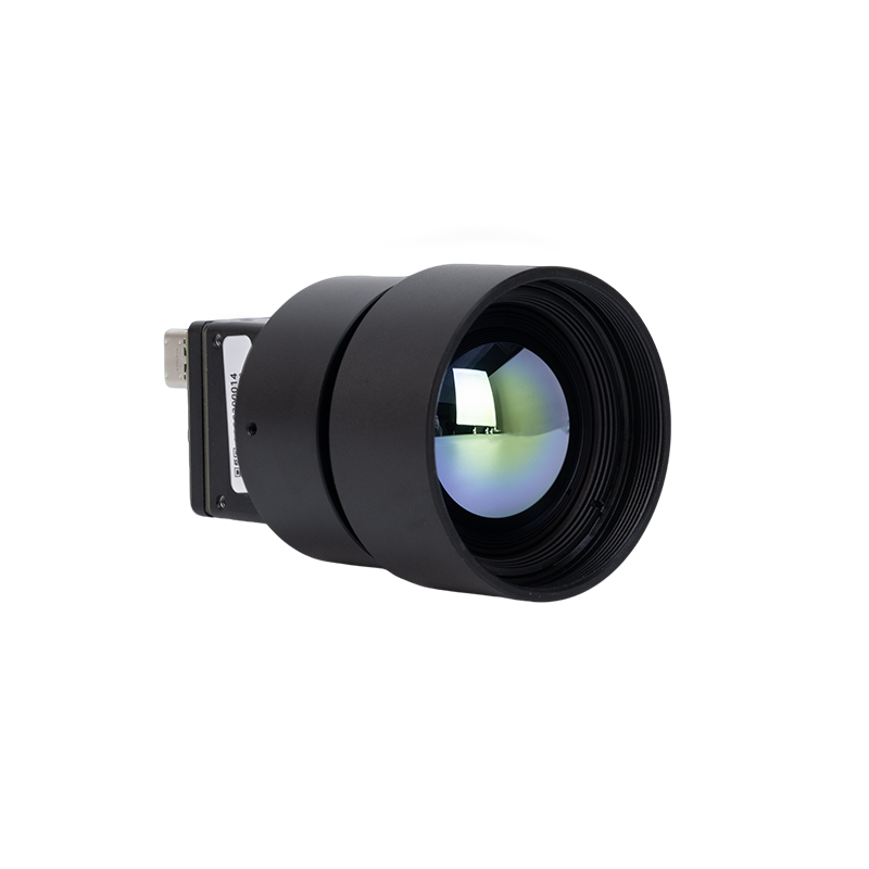
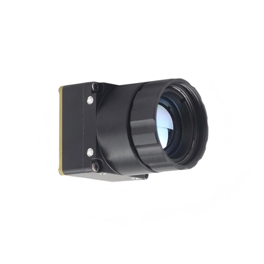
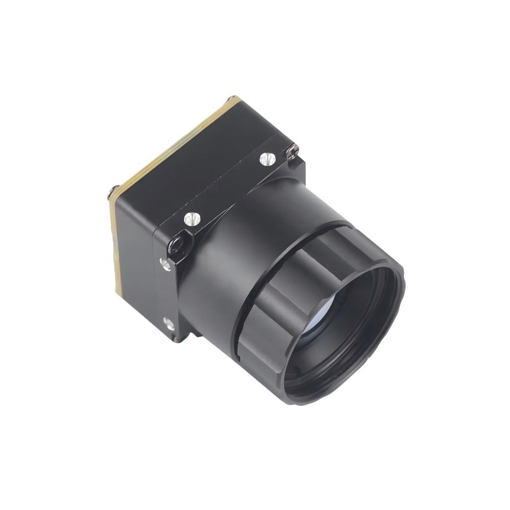
High Resolution Uncooled Infrared 1280*1024 Thermal Imaging LWIR Camera
Designed for ultra-demanding aerospace, defense, and wide-area industrial monitoring deployments, this high-definition uncooled thermal camera provides unmatched spatial resolving capability. Built around a large-format 1280×1024 VOx microbolometer array with a fine 12 µm pixel pitch, it captures four times the spatial radiometric data of standard 640×512 sensors. It comes paired with an integrated 25 mm high-aperture monocrystalline Germanium lens assembly to resolve micro-thermal deltas across broad physical perimeters and high-density industrial switchyards.
| Sensor Array Architecture | Uncooled VOx Microbolometer FPA |
| Native Array Resolution | 1280 × 1024 pixels (SXGA) |
| Pixel Pitch | 12 µm |
| Optical System Configuration | 25 mm Lens (Germanium Optics, DLC Coated) |
| Spectral Response Band | 8.0 µm to 14.0 µm (LWIR) |
| Thermal Sensitivity (NETD) | ≤ 40 mK at f/1.0, 25°C |
| Primary Applications | Perimeter Defense, Automated Substation Auditing, High-End Radiometric R&D |
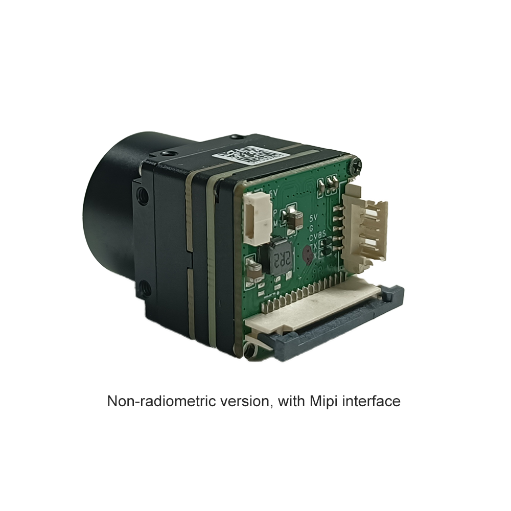
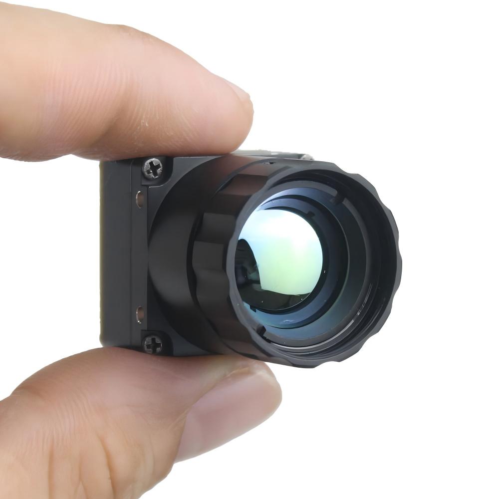
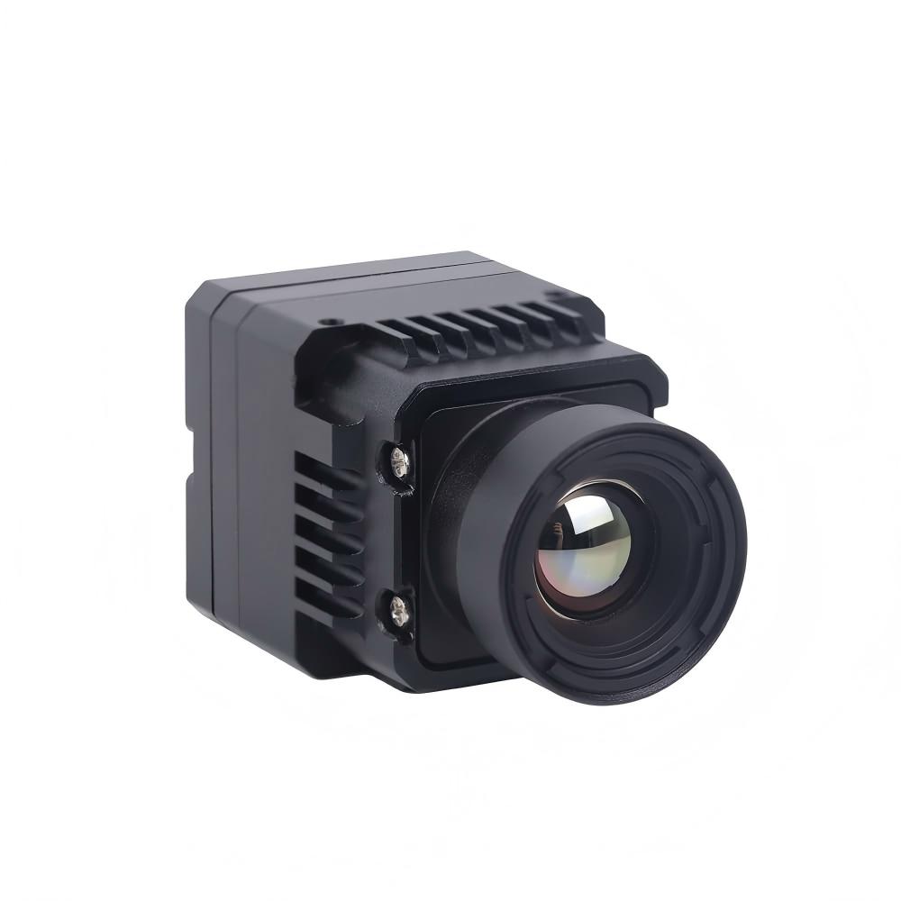
Uncooled Infrared MIPI 640/384/256 9mm Thermal Imaging Camera Module For Drones (Mini2)
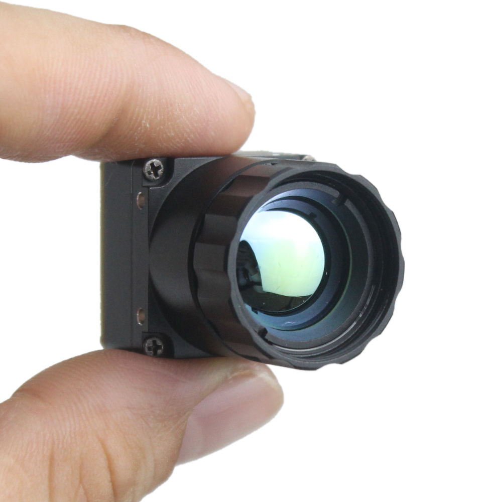
The Mini2 is an ultra-compact, low-cost uncooled infrared thermal imaging module engineered specifically for micro-UAV gimbals, robotic systems, and wearable tactical vision. Delivering sharp, crisp image presentation with ultra-low thermal noise, the module is available in native resolutions of 640×512, 384×288, or 256×192. Featuring a compact 9 mm athermalized lens and native MIPI CSI-2 interface compatibility, the Mini2 streams real-time radiometric telemetry directly into onboard edge-AI processors with minimal power consumption and weight.
| Core Designation | Mini2 Micro Uncooled Thermal Engine |
| Available Native Resolutions | 640 × 512 | 384 × 288 | 256 × 192 |
| Optics Focal Length | 9 mm Athermalized Lightweight Lens |
| System Interface Protocols | MIPI CSI-2 Direct-to-SoC, DVP, USB Expansion |
| Design Profile (SWaP) | Ultra-Compact, Lightweight Micro Profile (<30g payload) |
| Integration Compatibility | NVIDIA Jetson, NXP, Raspberry Pi CM4 Edge Boards |
| Primary Target Markets | Micro-UAV Payloads, Firefighter Handheld HUDs, Edge-AI Industrial Inspection |
6. OEM Thermal Core Selection Matrix
Selecting an infrared thermal imaging camera core requires balancing mission requirements against mechanical, optical, and thermal constraints. The table below outlines key trade-offs between high-resolution static/pedestal architectures (1280×1024) and lightweight aerial/edge modules (Mini2 640×512):
| Engineering Parameter | 1280×1024 25mm Enterprise Core | Mini2 640×512 9mm Drone Module |
|---|---|---|
| Native Pixel Count | 1,310,720 pixels (Superb spatial definition) | 327,680 pixels (Standard tactical resolution) |
| Weight & SWaP Budget | Suited for pan-tilt pedestals & heavy gimbals (>150g) | Optimized for micro-UAVs and hand-held devices (<30g) |
| Typical Power Draw | 2.0 W to 3.5 W (Continuous image processing) | ≤ 1.0 W (Optimized for extended battery runtimes) |
| Primary Interconnect | Industrial Digital Bus, Camera Link, USB 3.0 | Direct MIPI CSI-2, Parallel DVP, USB expansion |
| DRI Range Profile | Extended detection: vehicles >3.0 km, human >1.5 km | Tactical close/medium range: human ≈ 400m to 600m |
| NUC Calibration Loop | Precision electromechanical shutter calibration | Micro-shutter with dynamic shutterless algorithms |
Systems integrators targeting long-range identification through smoke or perimeter tracking will benefit most from the native resolving power of the 1280×1024 array. In contrast, aerial robotics, micro-UAVs, and wearable firefighter gear require the light payload weight and low power consumption of the Mini2 MIPI module to maximize flight and operational endurance.

7. Deep-Dive Technical FAQ
What is the fundamental difference between infrared photography and thermal imaging?
Conversely, an infrared thermal imaging camera operates in the Long-Wave Infrared spectrum (LWIR, spanning 8.0 to 14.0 µm). It measures intrinsic thermal radiation emitted directly by matter as a result of its thermodynamic temperature, as described by Planck's Law and the Stefan-Boltzmann Law. Operating without any ambient light, thermal cameras utilize specialized microbolometer focal plane arrays (typically Vanadium Oxide) housed behind anti-reflective coated Germanium optics to passively transform thermal flux into calibrated radiometric temperature matrices.
Are sub-$400 consumer thermal cameras actually worth buying for technical work?
This digital interpolation creates synthetic data points rather than recording genuine physical radiance. In technical diagnostic workflows, this smoothing blends localized high-temperature anomalies into surrounding cooler regions, often obscuring dangerous overheating conditions on printed circuit boards or high-resistance electrical terminals. Furthermore, cheap plastic or silicon chalcogenide optics can drift out of calibration under variable ambient temperatures. Professional engineering workflows require a minimum native resolution of 640×512 or 1280×1024, coupled with a sensitivity of ≤ 40 mK, to ensure every captured pixel represents real, calibrated radiometric data.
How do infrared thermal cameras cut through dense fog, smoke, and night conditions?
LWIR thermal cameras operate at wavelengths between 8.0 and 14.0 µm—substantially larger than the diameter of most smoke and fine particulate suspensions. As a result, the scattering cross-section is dramatically lower, allowing thermal radiation to pass through obscurants with minimal attenuation. Furthermore, because thermal sensors detect self-emitted radiation rather than reflected ambient light, they perform consistently in complete darkness without requiring active illumination that could bounce back and blind the detector.
📚 References & Further Reading
- ⚙️ Industry Standard: Microcontroller Interfacing & Low-Level Prototyping Standards at Arduino
- ⚙️ Industry Standard: High-Performance Embedded Vision Carrier & Interface Boards at Waveshare
- ✅ Related Guide: Can We Convert a Standard Camera into an Infrared Thermal Imaging System?
- ✅ Related Guide: Selecting the Optimal LWIR Thermal Camera Module: An OEM Edge Guide
- ✅ Related Guide: Compact Thermal Camera Modules for Micro-UAV and Drone Gimbals