
Infrared Thermal Imaging Camera Guide: Real Resolution, Sensor Tech & Buying Truths
2026年10月22日
The Ultimate Thermal Imaging Device Guide: Pro Performance, Edge AI & Practical ROI
2026年10月23日
Thermal Camera for Android: Pro Smartphone Attachments vs. Standalone Modules Guide
The convergence of uncooled Long-Wave Infrared (LWIR) microbolometers with modern mobile architectures has dismantled the barrier between high-cost military thermography and field-deployable commercial diagnostics. For decades, thermographic condition monitoring required bulky, proprietary handheld units running on closed operating systems. Today, the ubiquity of high-throughput USB Type-C ports, robust Android Open Source Project (AOSP) hardware abstraction layers (HAL), and low-power digital signal processing allows industrial engineers to convert standard enterprise smartphones and tablets into high-precision, multi-spectral thermal imagers.
However, selecting an enterprise-grade thermal camera for Android involves navigating complex engineering trade-offs. B2B systems architects and optical engineers must weigh plug-and-play USB dongles against low-level OEM core integrations, such as direct MIPI-CSI or embedded USB video class pipelines. Deciding between offloading thermographic computing to a commercial smartphone or deploying an integrated, galvanically isolated standalone core depends on your requirements for thermal sensitivity (Noise Equivalent Temperature Difference, or NETD), frame rate stability, raw radiometric pipeline access, and mechanical durability in harsh environments.
Table of Contents
- 👉 1. The Physics of Mobile LWIR: Sensor Architecture & Bandwidth
- 👉 2. Android Interfacing: USB-C OTG vs. Direct MIPI-CSI Cores
- 👉 3. Architectural Comparison: Plug-in Dongles vs. Standalone Handhelds vs. OEM Cores
- 👉 4. Critical Engineering Parameters: Resolution, Pixel Pitch, NETD & Optics
- 👉 5. Enterprise Product Comparison: High-Resolution Industrial Modules
- 👉 6. Software Pipeline: Android NDK, UVC Drivers, and Radiometric DSP
- 👉 7. Industrial Field Deployments: Power Systems, Diagnostics, and Drones
- 👉 8. Frequently Asked Questions (FAQ)
1. The Physics of Mobile LWIR: Sensor Architecture & Bandwidth
Thermal imaging operates in an entirely different electromagnetic spectrum than standard smartphone optical sensors. While typical CMOS visible-light image sensors detect wavelengths within the narrow optical band spanning from 380 to 740 nanometers (nm), industrial thermal sensors detect the Long-Wave Infrared (LWIR) band spanning 8 to 14 micrometers (μm). This physical reality means thermal imagers do not detect reflected ambient light; rather, they directly collect blackbody radiation emitted by all matter having a thermodynamic temperature above absolute zero (0 Kelvin), as governed by Planck’s Law and the Stefan-Boltzmann distribution.
Because ordinary silicate glass is completely opaque to electromagnetic radiation in the LWIR spectrum, an Android-connected thermal device cannot rely on standard phone lenses or common protective sapphire crystals. Instead, specialized optical elements engineered from single-crystal Germanium (Ge), Chalcogenide amorphous glass, or high-resistivity optical Silicon (Si) are required. These exotic materials are precision-lathed with diamond-turning tools and coated with broad-band anti-reflective (BBAR) layers to focus incoming electromagnetic heat flux onto a focal plane array (FPA) of microscopic heat sensors known as microbolometers.
The core sensing element inside modern mobile thermal attachments relies on either Vanadium Oxide (VOx) or Amorphous Silicon (α-Si) thin-film resistors suspended over a silicon Readout Integrated Circuit (ROIC) via microscopic micro-bridges. When an incident photon in the 8 to 14 μm spectrum strikes a microbolometer pixel, the suspended absorbing layer captures the infrared flux. This absorption elevates the thermodynamic temperature of the microscopic bridge structure. Because the sensing film possesses a pronounced Temperature Coefficient of Resistance (TCR), this minute thermal change induces a measurable variation in electrical resistance. Vanadium Oxide is the industrial gold standard, yielding a TCR of approximately -2% to -3% per Kelvin, which delivers significantly higher signal-to-noise ratios (SNR) than Amorphous Silicon alternatives.
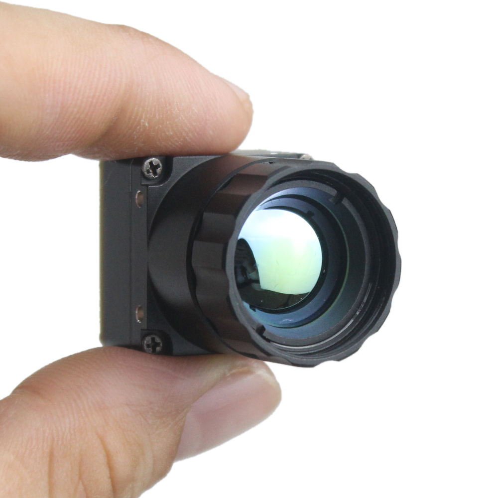
The underlying ROIC applies a stabilized micro-bias voltage, scanning the array line by line to convert micro-ampere variations into raw digital counts (Digital Numbers, or DN). Unlike laboratory-grade cooled thermal detectors that require bulky cryogenic Stirling coolers to chill indium antimonide (InSb) or mercury cadmium telluride (MCT) sensors down to 77 Kelvin, modern mobile solutions utilize uncooled, TEC-less (Thermo-Electric Cooler-less) microbolometer technology. Operating without active temperature stabilization means the sensor array is subject to thermal drift caused by the host smartphone's internal battery, mainboard processor heat dissipation, and fluctuating ambient weather conditions. To maintain measurement accuracy, the camera system incorporates periodic Non-Uniformity Correction (NUC) algorithms paired with an integrated electromechanical mechanical shutter that temporarily blocks the optical path to re-zero pixel offset matrices.
Engineers seeking deeper insights into high-throughput cores can review our comprehensive guide on high-performance 640 and 384 LWIR thermal camera cores to understand how different FPA layouts handle thermal drift in mission-critical environments.
2. Android Interfacing: USB-C OTG vs. Direct MIPI-CSI Cores
Connecting an LWIR sensor array to the Android operating system presents serious engineering challenges concerning throughput, bus latency, power supply integrity, and driver architecture. Developers and systems integrators generally evaluate two primary physical and logical interfaces: the universal USB-C On-The-Go (OTG) pipeline utilizing the USB Video Class (UVC) protocol, or direct chip-to-chip Mobile Industry Processor Interface Camera Serial Interface (MIPI-CSI) lines. For embedded architectures, selecting certified high-reliability connectors from manufacturers like Amphenol ensures that high-frequency clock lines and raw video data frames do not suffer from signal degradation or ground bounce during intensive thermal sweeps.
The USB-C OTG interface using UVC profiles represents the dominant transport layer for consumer-grade and prosumer commercial dongles. In this topology, the microbolometer FPA feeds its raw analog variations to an onboard Field-Programmable Gate Array (FPGA) or dedicated Application-Specific Integrated Circuit (ASIC) located within the external camera housing. This onboard processor executes initial Non-Uniformity Correction, applies dead-pixel concealment, packages the frame into a digital bitstream, and routes it through an onboard USB controller. When plugged into an Android smartphone, the device presents itself as a standard video source over the Linux kernel's Video4Linux2 (V4L2) driver framework.
While USB-C OTG offers universal plug-and-play capability across millions of commercial off-the-shelf (COTS) Android devices, it introduces significant technical overhead. Standard UVC video pipelines are fundamentally designed for 8-bit YUV or RGB consumer video streams. However, industrial radiometric thermography requires an absolute minimum of 14-bit or 16-bit uncompressed digital data per pixel to compute true temperatures across wide dynamic ranges without severe quantization distortion. Consequently, developers must bypass standard Android Camera2 APIs. They must use low-level Android USB Host APIs (android.hardware.usb) or compile custom Linux LibUSB user-space drivers through the Android Native Development Kit (NDK) to extract 16-bit packed data arrays (such as the Y16 video format) through custom vendor bulk endpoints.
Conversely, the direct MIPI-CSI architecture connects the thermal imaging module straight to the Camera Serial Interface receiver of the host System-on-Chip (SoC). Prototyping teams often validate these high-speed CSI trace lines and physical breakout connections using hardware interface adapters and expansion kits from developers like Waveshare. In this configuration, the raw sensor output is transmitted across low-voltage differential signaling pairs (D-PHY lanes) directly into the host processor's Image Signal Processor (ISP) subsystem. This method eliminates the latency, power-hungry protocol conversion, and physical bulk of intermediate USB bridge controllers.
The trade-offs between these two interfacing philosophies are distinct:
- ⚙️ Direct MIPI-CSI Throughput: Yields the absolute lowest frame-to-display latency (frequently under 1 millisecond), drops power consumption by up to 40% relative to USB bridges, and eliminates cable clutter, making it the premier choice for custom military tablets, UAV gimbals, and automated robotic systems.
- ⚙️ Board Support Package Overhead: MIPI integrations demand deep Linux kernel customizations, including custom device tree source (DTS) overlays, proprietary V4L2 sensor sub-device drivers, and dedicated hardware board respins.
- ✅ USB-C OTG Interoperability: Ensures instant zero-solder hardware compatibility across hundreds of Android smartphone models, field tablets, and external diagnostic computers, minimizing deployment barriers for dispersed field operations.
- ⚙️ USB Bus Saturation & Jitter: Transmitting uncompressed 640 × 512 radiometric arrays at 16-bit depth and 50 Hz requires sustained bandwidth exceeding 260 Mbps, pushing the limits of shared USB 2.0 PHY buses common on entry-level Android chipsets.
3. Architectural Comparison: Plug-in Dongles vs. Standalone Handhelds vs. OEM Cores
Specifying a thermal imaging solution requires a complete evaluation of the operational environment, mechanical stresses, user ergonomics, and lifecycle maintenance costs. Industrial condition monitoring can be deployed through three major structural form factors: smartphone plug-in dongles, dedicated standalone handheld imagers, and embedded OEM thermal camera cores.
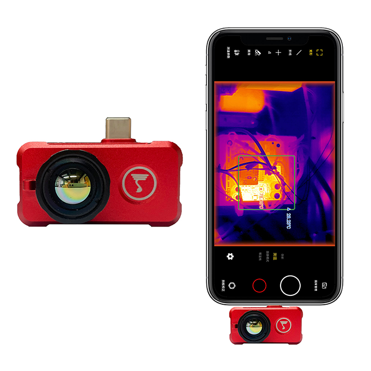
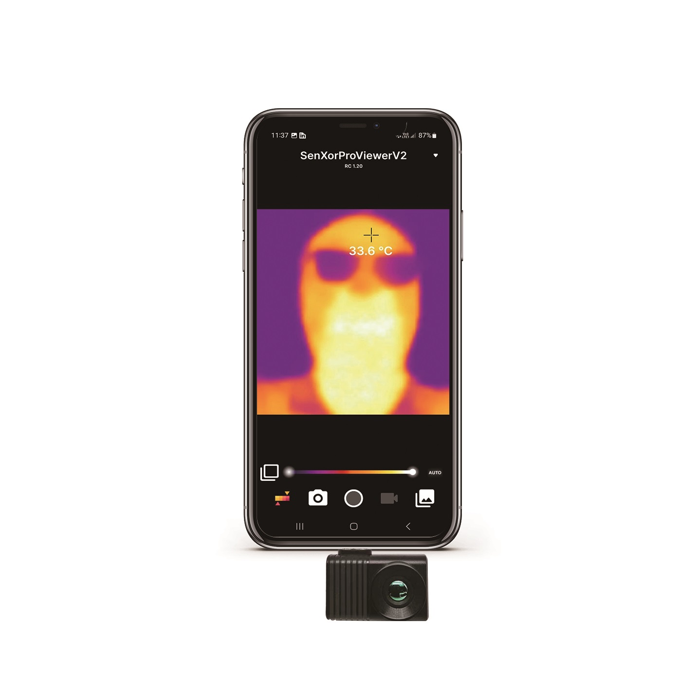
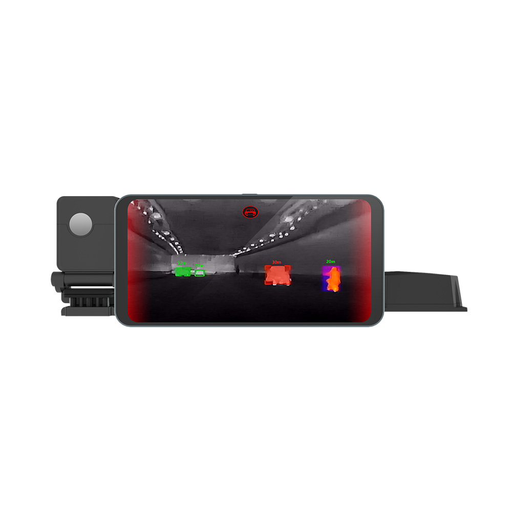
Smartphone plug-in dongles are ultra-compact peripherals that plug directly into an Android smartphone's bottom USB-C port. These units take advantage of the smartphone's high-resolution OLED screen, fast multi-core application processor, internal GPS module, and cellular/Wi-Fi radios. By shifting display rendering, cloud synchronization, and reporting tasks to the smartphone, hardware manufacturers can offer high-resolution thermal imaging at accessible price points. Maintenance personnel can capture a thermal image and immediately email a complete radiometric report directly from the plant floor.
However, mobile dongles carry mechanical and electrical vulnerabilities in harsh industrial settings. When a smartphone with an attached thermal dongle is dropped, the rigid USB-C connector acts as a mechanical lever, transferring destructive torsional force directly into the smartphone’s surface-mounted mainboard connector. This can permanently break the device's physical port. Furthermore, the dongle draws power directly from the host phone battery via USB-C power delivery, which can drain a typical mobile device in under two hours of continuous scanning. In environments with heavy dust, water exposure, or explosive atmospheres, standard commercial smartphones cannot meet IP67 or ATEX/IECEx Zone 1/2 intrinsic safety ratings.
Standalone industrial handheld imagers combine the optical lens, microbolometer, dedicated image processor, display screen, ergonomic pistol grip, and isolated rechargeable battery pack into an integrated, rugged housing. These enterprise-grade instruments feature drop-tested enclosures rated for 2-meter drops onto concrete, physical buttons designed for operation while wearing heavy protective gloves, and dedicated optical paths that frequently include secondary visible-light cameras for dynamic multispectral image blending. The trade-off lies in software rigidity and hardware cost: standalone thermal cameras feature high capital acquisition costs, sluggish user interfaces based on older real-time operating systems, slow touch response, and cumbersome manual data export procedures via SD cards or proprietary desktop software.
Embedded OEM thermal cores represent the raw building blocks of modern thermographic engineering. Stripped of external housings, consumer displays, and batteries, an OEM core consists purely of the optical lens assembly, the VOx microbolometer focal plane array, and an integrated digital processing board delivering digital video via MIPI, USB, or parallel LVDS. These modules are specifically engineered for mechanical integration into bespoke industrial platforms, including custom ruggedized enterprise Android tablets, autonomous ground vehicles (UGVs), pan-tilt-zoom perimeter surveillance systems, and high-altitude surveillance drones. For installations requiring mechanical stabilization against high vibration, these cores are integrated into specialized enclosures such as tri-axis stabilized thermal pan-tilt systems to ensure stable imagery under extreme dynamic loads.
4. Critical Engineering Parameters: Resolution, Pixel Pitch, NETD & Optics
Evaluating an engineering datasheet for an uncooled LWIR thermal module requires understanding the interdependencies between optical engineering, solid-state physics, and signal processing. Four critical parameters dictate the actual real-world performance, image sharpness, and measurement accuracy of an Android-compatible thermal imaging system.
The first fundamental parameter is the native Focal Plane Array (FPA) spatial resolution. In thermal imaging, resolution defines the physical number of microbolometer detector elements fabricated on the silicon substrate. Typical industry classifications include:
- ⚙️ Entry-Level Industrial (256 × 192 = 49,152 active pixels): This resolution provides sufficient spatial fidelity for close-proximity inspections, such as benchtop printed circuit board (PCB) troubleshooting, residential energy auditing, mechanical bearing checks, and small electrical breaker panel audits.
- ⚙️ Mid-Tier Professional (384 × 288 = 110,592 active pixels): Delivering more than double the pixel count of entry-level units, this category represents the industrial standard for predictive plant maintenance, mechanical vibration diagnostics, and building envelope assessments.
- ⚙️ High-Definition Enterprise (640 × 512 = 327,680 active pixels): Designed for long-range inspection tasks, aerial utility line sweeps, high-voltage switchgear monitoring, search-and-rescue operations, and military target acquisition. High resolution allows operators to resolve tiny thermal anomalies on small targets from safe standoff distances.
Engineers can find more detailed guidance on selecting appropriate sensor geometries by reading our in-depth article on selecting high-resolution thermal imaging modules for tactical and industrial architectures.
The second parameter is the detector pixel pitch, measured in micrometers (μm). Pixel pitch refers to the physical center-to-center distance between individual microbolometer sensing cavities. Over the past decade, the industry standard has shifted from legacy 25 μm and 17 μm architectures down to 12 μm nodes, with cutting-edge foundries actively fabricating 10 μm arrays. Migrating to a smaller 12 μm pixel pitch reduces the physical dimensions of the silicon die for a given resolution. This reduction allows optical engineers to use significantly smaller Germanium objective lenses while maintaining equivalent focal lengths, field-of-view (FOV), and instantaneous field-of-view (iFOV) figures. Consequently, 12 μm technology is the direct engineering enabler behind ultra-compact thermal modules that interface seamlessly with Android hardware without unbalanced physical overhang.
The third parameter is Noise Equivalent Temperature Difference (NETD), expressed quantitatively in milliKelvins (mK). NETD is a standardized figure of merit that establishes the thermal sensitivity of the system. It defines the temperature difference on an ideal blackbody radiator that generates a signal equal to the internal electronic noise floor of the microbolometer and ROIC signal chain (SNR = 1). Lower values indicate greater thermal sensitivity. A sensor with an NETD rating of less than 50 mK is considered acceptable for baseline industrial diagnostics, while values under 40 mK or 30 mK represent high-performance instrumentation. High sensitivity allows an engineer to visualize extremely subtle thermal gradients, such as moisture tracking beneath concrete structures, minor cooling inefficiencies in semiconductor packages, and early-stage insulation breakdowns long before catastrophic equipment failure.
The fourth parameter is the operational refresh rate, measured in Hertz (Hz). Due to international defense regulations, specifically the Wassenaar Arrangement and US Export Administration Regulations (EAR), thermal imaging devices operating at refresh rates equal to or exceeding 9 Hz are classified as dual-use goods subject to strict export licensing. As a result, many budget consumer Android dongles are artificially locked to an 8.6 Hz or 9 Hz output. While a 9 Hz sensor is usable for static, stationary inspections, it causes severe image lag, temporal tearing, and operator disorientation when panning across complex industrial environments. For robotics, dynamic machinery audits, vehicle navigation, and drone-mounted tracking, a high frame rate of 25 Hz, 30 Hz, or 50 Hz is essential to guarantee blur-free visual monitoring and real-time radiometric alerting.
5. Enterprise Product Comparison: High-Resolution Industrial Modules
When selecting high-performance thermal imaging cores for integration with Android platforms, single-board computers (SBCs), or autonomous drone gimbals, engineering teams must evaluate raw sensor performance against physical size, weight, power, and cost (SWaP-C) constraints. Below are two industry-grade OEM thermal cores engineered specifically for advanced integration.
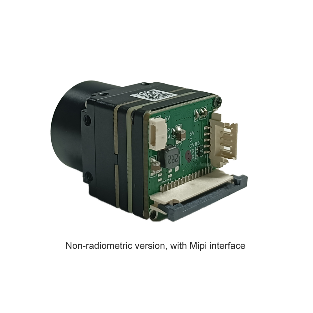
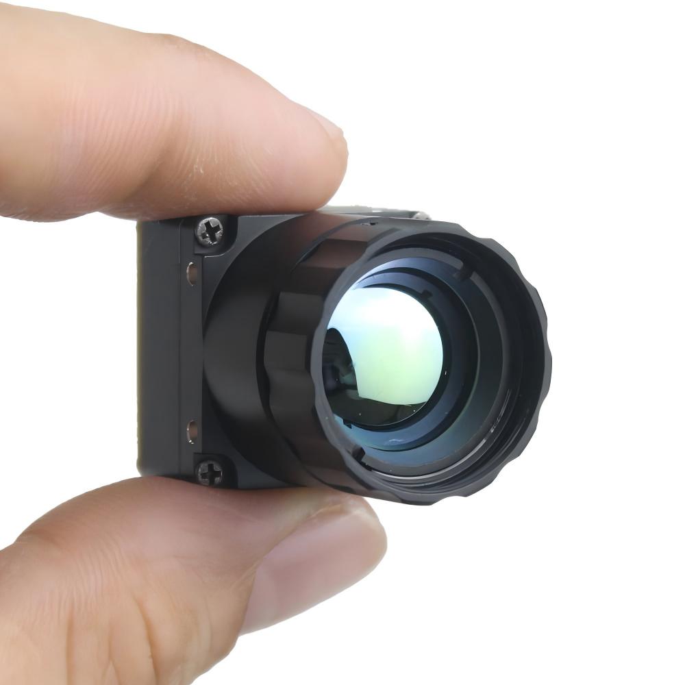
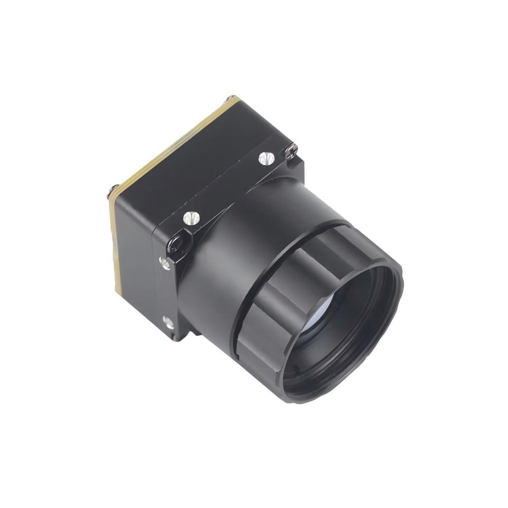
Uncooled Infrared Mini2 640x512 9mm Thermal Imaging Camera Module For Drones
The Mini2 640x512 module provides high spatial resolution within an ultra-compact, low-power form factor. Built around a sensitive uncooled Long-Wave Infrared focal plane array, this core delivers sharp image presentation, low latency, and dependable continuous operation for mission-critical unmanned aerial vehicles and embedded surveillance systems.
- ⚙️ Native Thermal Resolution: 640 × 512 pixels
- ⚙️ Optical Assembly: 9mm high-transmission Germanium lens
- ⚙️ Spectral Range: 8 to 14 μm (LWIR)
- ⚙️ Physical Profile: Mini uncooled package designed for aerial gimbals and compact systems
- ⚙️ Primary Interfaces: Direct MIPI output and embedded USB data streams
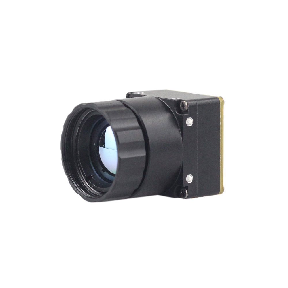
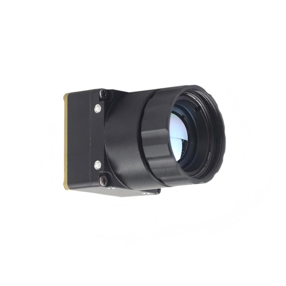
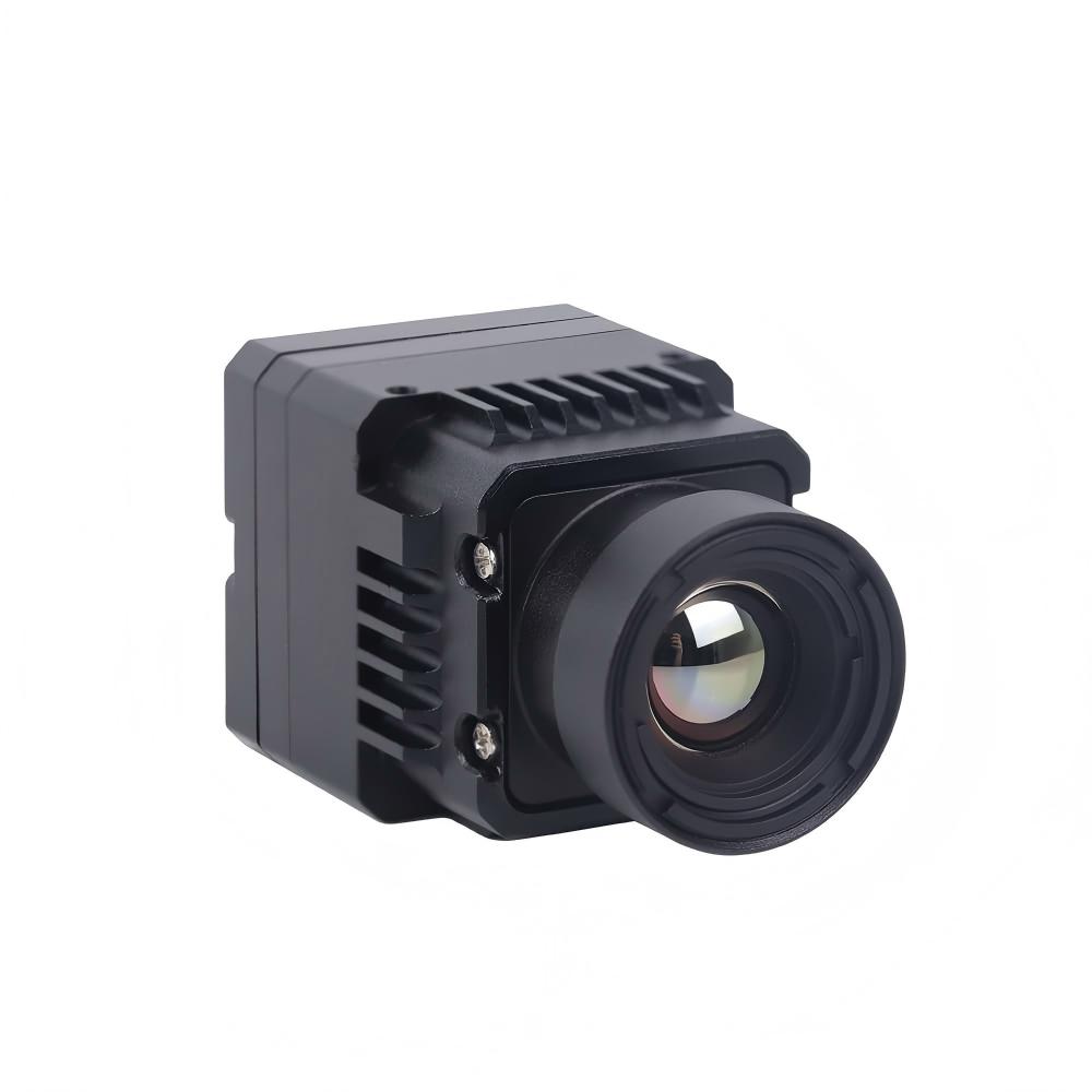
Uncooled LWIR Mini 256*192 Thermal Imaging Camera Module Similar To DJI For Detecting Mines
Engineered for precise thermodynamic measurement, the Mini 256 uses a high-performance infrared detector array to generate ultra-clear thermal imagery with uniform radiometric temperature reporting. Its compact architecture makes it ideal for mine detection payloads, custom handheld mobile attachments, and industrial robotic systems.
- ⚙️ Native Thermal Resolution: 256 × 192 pixels
- ⚙️ Sensor Architecture: High-performance uncooled LWIR microbolometer
- ⚙️ Radiometric Output: Full-frame temperature measurement matrix
- ⚙️ Application Design: Optimized for mine detection, structural surveys, and smart industrial automation
- ⚙️ Interface Compatibility: USB / serial digital interface, ideal for host Android configurations
The table below provides a side-by-side engineering comparison of these two high-performance modules to help systems architects select the optimal core for their Android hardware stack:
| Engineering Metric | Mini2 640x512 9mm Drone Module | Mini 256x192 Mine Detection Module |
|---|---|---|
| Detector Core Type | Uncooled VOx Microbolometer | Uncooled LWIR Microbolometer |
| Native FPA Resolution | 640 × 512 (327,680 pixels) | 256 × 192 (49,152 pixels) |
| Optical Configuration | 9mm Germanium Single-Field Lens | Compact Athermalized Radiometric Lens |
| Wavelength Coverage | 8 to 14 μm (LWIR) | 8 to 14 μm (LWIR) |
| Radiometric Capability | Advanced qualitative/radiometric profiling | Full radiometric per-pixel temperature reporting |
| Form Factor & Mass | Miniaturized, ultra-lightweight drone layout | Micro footprint for handhelds & mine detection |
| Target Android Architecture | Direct MIPI / USB to Drone Companion Computers | USB-C to Android Smartphones & Field Tablets |
6. Software Pipeline: Android NDK, UVC Drivers, and Radiometric DSP
Developing custom software for an Android thermal imaging system requires processing raw radiometric data beyond standard Android Camera2 APIs. While standard smartphone cameras output three 8-bit channels representing Red, Green, and Blue color spaces, thermal camera cores output a single high-dynamic-range stream of 14-bit or 16-bit raw digital integers for every pixel in the focal plane array. Processing this raw datastream in real time on mobile architectures demands an optimized computing pipeline using the Android Native Development Kit (NDK) with C and C++.
The processing chain begins at the kernel and driver abstraction layer. When a thermal camera module is connected via USB-C, standard high-level Java and Kotlin Android frameworks cannot directly ingest raw 16-bit packed frames without truncating the dynamic range. Modern systems use native C libraries like libusb or direct Video4Linux2 (V4L2) ioctl system calls compiled inside the NDK environment to stream the raw frame packets into shared memory ring buffers. This prevents Android's garbage collection cycles from causing dropped frames or high bus jitter.
Once the raw frame array arrives in the native C++ layer, digital signal processing (DSP) algorithms execute several calibration operations:
- ⚙️ 1. Two-Point Non-Uniformity Correction (NUC): Gain and offset correction factors are applied across every individual microbolometer pixel. This compensates for natural physical variations in pixel manufacturing and sensor drift caused by the host phone's internal heat generation.
- ⚙️ 2. Dead-Pixel Concealment: Because commercial microbolometers may contain non-functional or unstable pixels, spatial interpolation routines calculate running averages from surrounding healthy pixels to eliminate visual artifacts.
- ⚙️ 3. Planck Equation Radiometric Transformation: The corrected 14-bit or 16-bit Digital Number (DN) values are converted into absolute thermodynamic temperature values (in Kelvin) using the inverted Planck equation:
Temperature = B / ln(R / (DN - O) + F)Here, constants R, B, and F represent factory-calibrated radiometric Planck constants stored within the core's non-volatile EEPROM, and O represents the calculated shutter offset. The software must also correct for real-world environmental variables, including surface emissivity, reflected ambient background temperature, atmospheric transmission loss, and ambient relative humidity.
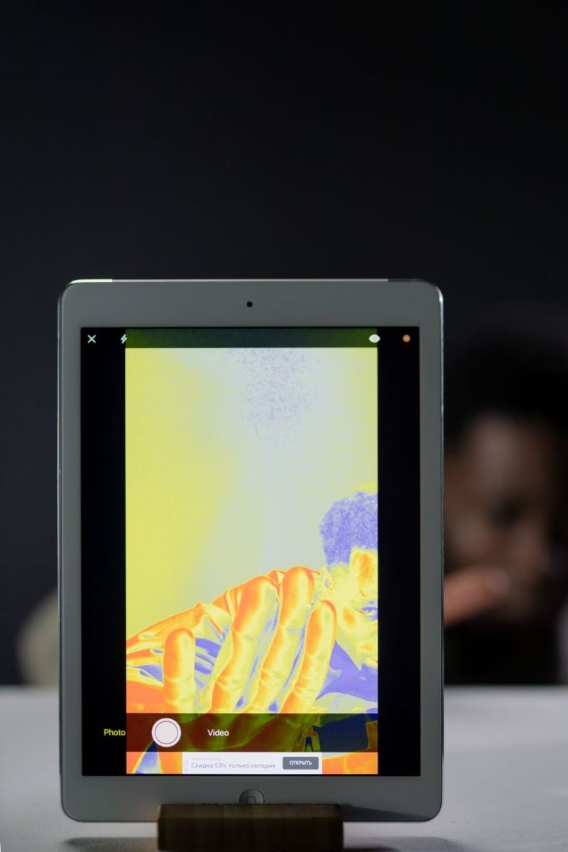
After calculating the full radiometric temperature array, the system renders the scene on the Android user interface. Directly downscaling 14 bits of dynamic data (values from 0 to 16,383) into an 8-bit display format (values from 0 to 255) through linear compression flattens local scene contrast, making subtle thermal variations invisible. To solve this, developers write GPU fragment shaders using OpenGL ES 3.0 or Vulkan. These shaders execute dynamic range partitioning and Contrast-Limited Adaptive Histogram Equalization (CLAHE). The equalized single-channel scalar values are then mapped across specialized false-color lookup tables (LUTs)—such as Ironbow, White-Hot, Black-Hot, Jet, or Rainbow—before being composited onto the Android UI layout via a high-performance SurfaceView or Jetpack Compose native canvas.
7. Industrial Field Deployments: Power Systems, Diagnostics, and Drones
Deploying mobile, Android-connected thermal imaging platforms provides industrial maintenance teams with real-time diagnostic capabilities across diverse field environments.
In high-voltage electrical installations and utility substations, field engineers face energized systems operating under extreme electrical stress. Loose terminal connections, phase imbalances, corroded busbars, and degraded transformer bushings all produce distinct localized Joule heating (I²R resistive losses). Using an Android smartphone equipped with an uncooled thermal module, an engineer can inspect switchgear cabinets from a safe standoff distance beyond dangerous flashover boundaries. Utilizing the smartphone's integrated touch display, the inspector can tap specific high-voltage connections to establish active radiometric spot meters, tracking peak temperature rises (ΔT) above ambient reference baselines to flag critical maintenance priorities.
In electronics engineering and quality assurance laboratories, thermal modules with specialized macro lenses serve as essential micro-diagnostic tools. Modern multi-layer printed circuit boards feature surface-mount components, ball grid array (BGA) packages, and voltage-regulator modules (VRMs) that can fail silently due to internal short circuits or thermal runaway. An Android tablet mounted to a PCB inspection stand provides high-magnification thermal imaging, allowing hardware developers to locate shorted ceramic capacitors pulling excessive micro-amperes. The Android software can graph thermal rise curves over time, helping engineers identify localized heating issues during dynamic chip load cycles.
In aerial robotics and field demining, compact OEM modules like the Mini2 640 and Mini 256 deliver significant operational value. Because uncooled LWIR cores feature minimal mass and low power draw, they mount cleanly inside brushless 3-axis drone gimbals without degrading flight times. Search teams and combat engineers deploy these aerial platforms to detect buried sub-surface landmines and improvised explosive devices (IEDs). Soil directly above disturbed earth or buried metallic casings displays distinct thermodynamic heating and cooling rates compared to surrounding undisturbed ground. During natural diurnal temperature cycles (such as sunrise and sunset), aerial Android thermal mapping systems reveal the distinctive surface thermal footprints of buried munitions, keeping human teams safely outside active danger zones.
THERMAL IMAGING REAL-TIME VIDEO
8. Frequently Asked Questions (FAQ)
Can an Android app turn my phone into a thermal camera without extra hardware?
Should I choose a plug-in Android thermal camera or a dedicated standalone imager?
What specifications make a good value thermal camera module for Android?
📚 References & Further Reading
- Industry Standard: High-reliability connectivity and fine-pitch interface solutions engineered by Amphenol
- Industry Standard: Embedded hardware modules and edge computing prototyping tools from Waveshare
- Related Guide: High-Performance 640 & 384 LWIR Thermal Camera Cores Selection Guide
- Related Guide: High-Resolution Thermal Imaging Module Selection and Optimization (Arabic Resource)
- Related Guide: Tri-Axis Stabilized Gimbal Thermal Camera Integration (Arabic Resource)