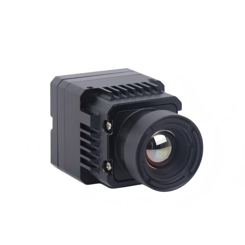
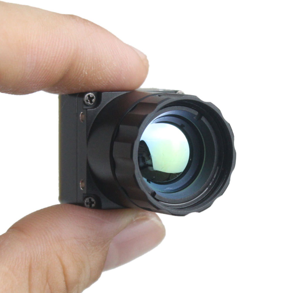
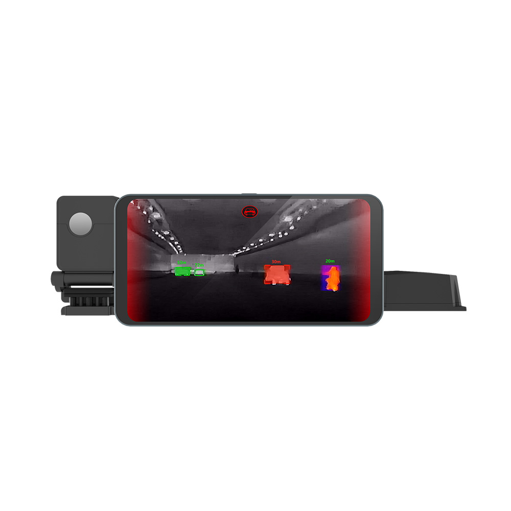

640*512/9.1 Thermal Imaging Camera Module: High-Res Drone Integration Guide
2026年7月13日
How to Choose the Right Industrial Thermal Camera Module for AI & Edge Integration
2026年7月14日
# High-Definition Infrared Thermal Module with CVBS: The Ultimate Integration Guide for FPV, Drones, and Edge AI
The demands of modern tactical aerial platforms, remote pilotage (FPV), and distributed Edge AI nodes have pushed sensor payloads to their physical limits. Historically, system integrators faced a punishing compromise: accept the weight, latency, and power penalties of heavy digital-to-analog converter boards, or sacrifice thermal target acquisition range by using low-resolution, legacy analog sensors. Finding a payload that balances thermal sensitivity with native, low-latency transmission interfaces has remained the Holy Grail for aerospace engineers, unmanned aerial vehicle (UAV) designers, and industrial automation architects alike.
This comprehensive technical blueprint analyzes how modern uncooled long-wave infrared (LWIR) cores bridged this gap by combining highly advanced high-definition digital focal plane arrays with native Composite Video Baseband Signal (CVBS) outputs. By utilizing system-on-chip (SoC) architectures driven by application-specific integrated circuits (ASICs), modern thermal modules execute real-time spatial noise reduction, digital detail enhancement, and analog signal serialization on a single, low-power PCBA. Whether you are building long-range search and rescue (SAR) searchlight drones, defense-grade micro-UAVs, or remote AI-driven edge networks, this guide provides the foundational engineering knowledge, raw signal physics, and integration methodologies required to deploy high-resolution thermal imaging systems over long distances without latency bottlenecks.
Table of Contents
- 👉 1. Engineering Architecture: Decoupling CVBS and Digital Thermal Cores
- 👉 2. The Digital Downscaling Mystery: High-Definition Arrays over Analog Pipes
- 👉 3. Comparative Product Specifications for Edge Systems
- 👉 4. Step-by-Step Hardware Integration & UAV Pinout Mapping
- 👉 5. Software Customization & SDK Deployment Guide
- 👉 6. Deep-Dive Engineered FAQ on CVBS & High-Definition Thermal Integration
---
1. Engineering Architecture: Decoupling CVBS and Digital Thermal Cores
To integrate thermal cores into highly optimized Edge AI platforms or long-range FPV aerial vehicles, it is critical to understand the separation between the digital sensing plane and the serial analog output plane. Modern uncooled infrared cores do not treat analog CVBS as a legacy afterthought. Instead, they implement parallel silicon processing pipelines designed to serve low-latency analog displays and high-fidelity digital processing units simultaneously. Here's the deal: if you don't map out this pipeline correctly, your system will suffer from dropped frames and analog signal jitter.

1.1 Physics of the 12μm Uncooled LWIR Microbolometer
Look, the core of an uncooled thermal sensor module contains a Focal Plane Array (FPA) consisting of uncooled microbolometers. These microbolometers are composed of active thin-film materials—typically Vanadium Oxide (VOx) or Amorphous Silicon (α-Si)—suspended as micromechanical bridges over a silicon read-out integrated circuit (ROIC) substrate. Each pixel behaves as a highly sensitive thermal resistor. When long-wave infrared radiation (8μm to 14μm) hits the active area, the FPA absorbs photons, raising its internal temperature. This temperature delta alters the absolute electrical resistance of the layer, defined by its Temperature Coefficient of Resistance (TCR).
The underlying ROIC measures this change in resistance by applying a stable bias voltage or current. The analog-to-digital converter (ADC) on the ROIC then digitizes the resulting values into high-bit raw digital data (typically 14-bit or 16-bit). Modern sensor cores use a 12-micrometer (12μm) pixel pitch. Moving from legacy 17μm arrays to 12μm sizes significantly reduces the physical layout of the silicon die. This design allows smaller optics to capture the same instantaneous field of view (IFOV), boosting spatial resolution while dramatically decreasing both system payload weight and thermal mass.
1.2 Understanding CVBS Signal Serialization and Latency Profiles
In the shop, we frequently see engineers struggling with latency budgets when designing real-time piloting systems (like UAVs or FPV drones). Traditional setups convert digital feeds to analog using external conversion boards, adding significant latency. Industrial composite video baseband signal (CVBS) outputs avoid this delay by operating directly on the sensor's processing board. The CVBS pipeline functions through several key steps:
- ⚙️ Raw Ingestion: The 14-bit or 16-bit digital frame from the microbolometer ROIC is processed inside the onboard ASIC.
- ⚙️ Direct Serialization: An integrated digital-to-analog converter (DAC) serializes the processed linear thermal data directly into a continuous analog voltage waveform. This matches NTSC (720 x 480 px at 29.97Hz) or PAL (720 x 576 px at 25Hz) timing requirements.
- ⚙️ Bypassing Software Steps: Because the ASIC converts this data internally, it bypasses operating-system frame buffers, network stack packaging, and external driver layers.
This hardware-level pipelining keeps the latency between IR photon capture and output CVBS analog serialization to a fraction of a frame buffer interval—frequently well below 10 milliseconds. Compare this to digital IP-based video streams (such as RTSP over 10/100M Ethernet), which require complex video compression algorithms (H.264/H.265) and network packet encapsulation. This overhead adds 80ms to over 250ms of network-induced latency, making real-time pilot navigation or high-speed intercept maneuvers virtually impossible.
1.3 Signal Paths and System Power Budgets
In remote, battery-powered Edge AI systems, the hardware design is highly constrained by the available power budget. You need to choose your interface chips based on direct power and thermal trade-offs:
- ✅ CVBS Only Configuration: The analog output driver remains exceptionally efficient. Driving a high-definition core (e.g., 640 x 512 resolutions) using an active CVBS driver draws only 0.8W to 1.2W. This preserves battery life on micro-UAVs.
- ✅ Dual-Output Hybrid Configuration (CVBS + MIPI-CSI2 or USB): In this configuration, the digital stream is routed directly to an on-board host micro-controller or neural processing unit (NPU) for high-level object detection, while the raw CVBS stream is simultaneously routed to an analog FPV transmitter (VTX). This dual architecture keeps system power draw to approximately 1.1W to 1.5W.
- ✅ Active IP / RTSP Module Configuration: Operating complex Ethernet physical layers (PHY) and RTSP compression pipelines on-board consumes significant power. These modules typically require 1.8W to 2.8W, making passive cooling essential for survival in confined industrial enclosures.
For drone integration and FPV designs, learn more about balancing DIY setups against professional-grade configurations in our detailed thermal camera module price guide.
---
2. The Digital Downscaling Mystery: High-Definition Arrays over Analog Pipes
One of the most persistent myths in thermal sensor integration is that utilizing a high-definition thermal array (640 x 512) over an analog CVBS pipe is a waste of resolution, citing the physical bandwidth limitations of PAL or NTSC formats. Let's bust this myth right now and look at how high-resolution sensors actually improve the final output.
2.1 Demystifying Sub-pixel Interpolation & Downscaling Algorithms
When a 640 x 512 pixel 14-bit digital thermal array is output through an analog CVBS controller, it must fit into an NTSC or PAL resolution. However, the system does not simply drop pixels or crop the image. Instead, the onboard ASIC processor uses real-time scaling algorithms:
- ⚙️ Spatial Downscaling: Instead of using basic nearest-neighbor downscaling (which causes aliasing and jagged edges), the ASIC uses spatial algorithms like bilinear, bicubic, or Lanczos interpolation. These mathematical functions combine information from multiple surrounding pixels to calculate the final value for the analog waveform.
- ⚙️ Anti-Aliasing Filter: The interpolation acts as a spatial low-pass filter, which eliminates high-frequency noise and reduces digital artifacts in the downscaled analog video.
- ⚙️ Signal-to-Noise Ratio (SNR) Gains: Combining neighboring pixels through downscaling serves as a spatial averaging filter. Averaging spatial data mathematically reduces random, non-correlated temporal noise (NETD) across the frame. Specifically, the new SNR is approximately equal to the original SNR multiplied by the square root of the cluster ratio of downscaled pixels. In practice, a downscaled 640 x 512 sensor output delivers a clean, low-noise analog image.
For a broader overview of how thermal imaging applies to non-industrial applications, check out our companion piece on thermal imaging as a practical life partner.
2.2 Advanced Digital Detail Enhancement (DDE) and Spatial Profiling
An analog signal is only as good as the contrast tuning running behind it. The ASIC processors in premium modules use special image processing algorithms to optimize the dynamic range before converting the signal to analog. First, the system splits the incoming 14-bit raw image into low-frequency and high-frequency content using a spatial bilateral filter, isolating small details without introducing halo artifacts at high-contrast edges.
Next, edge transitions, wire structures, and distant thermal signals are routed to the high-frequency path, where the system applies spatial amplification (Digital Detail Enhancement / DDE) to boost these faint thermal variations. Simultaneously, large thermal backgrounds (like soil, roads, and clouds) are processed in the low-frequency path, where the dynamic range is compressed to fit into an 8-bit output. Finally, the two channels are recombined, and the system runs an Adaptive Temporal Automatic Gain Control (AGC) loop to map the 8-bit dynamic range to output the clearest possible real-time analog video. This signal optimization allows operators to detect small targets—such as overhead powerlines, distant humans, or small thermal anomalies—even through a low-bandwidth composite analog signal.
2.3 Temperature Calibration, Drift Mitigation, and Radiometric Analysis
Industrial integrations often require radiometric analysis, which means measuring absolute temperature values directly from the thermal image. Maintaining this accuracy requires managing thermal drift inside the camera core. Uncooled LWIR FPAs are highly sensitive to their own internal temperature variations. Without compensation, heat buildup from the module's driving electronics will corrupt temperature measurements and degrade overall image quality.
To combat drift, the camera uses an internal mechanical shutter or an electrical shutterless calibration algorithm. During a Flat Field Correction (FFC) event, the shutter closes briefly to provide a uniform thermal reference across the array, allowing the system to recalculate its offset coefficients and restore a clean, noise-free image. To convert raw digital sensor values to actual temperatures in real time, the processor runs localized polynomial formulas mapping corrected pixel voltage values directly to temperature targets. This calculation allows Edge AI software platforms to monitor surface temperatures and detect thermal emergencies in real time.
For applications requiring precise thermography, integrating highly calibrated cores from industrial specialists like DFRobot ensures rock-solid SDK compatibility and long-term hardware reliability.
---
3. Comparative Product Specifications for Edge Systems
Developing high-end unmanned systems and Edge AI infrastructures requires selecting hardware with the exact electrical, optical, and physical specifications needed for the job. Below are the engineering details for two class-leading thermal modules featuring uncooled microbolometers.
3.1 Uncooled Infrared RJ45 CVBS RTSP IP 640*512 Thermal Camera Module
Specifically engineered for high-altitude UAV search and rescue, long-range security networks, and hybrid analog-digital Edge AI installations. This module is built around a powerful ASIC video engine that supports simultaneous RTSP digital streaming and zero-latency analog CVBS outputs.
Uncooled Infrared RJ45 CVBS RTSP IP 640*512 Thermal Sensor Camera Module
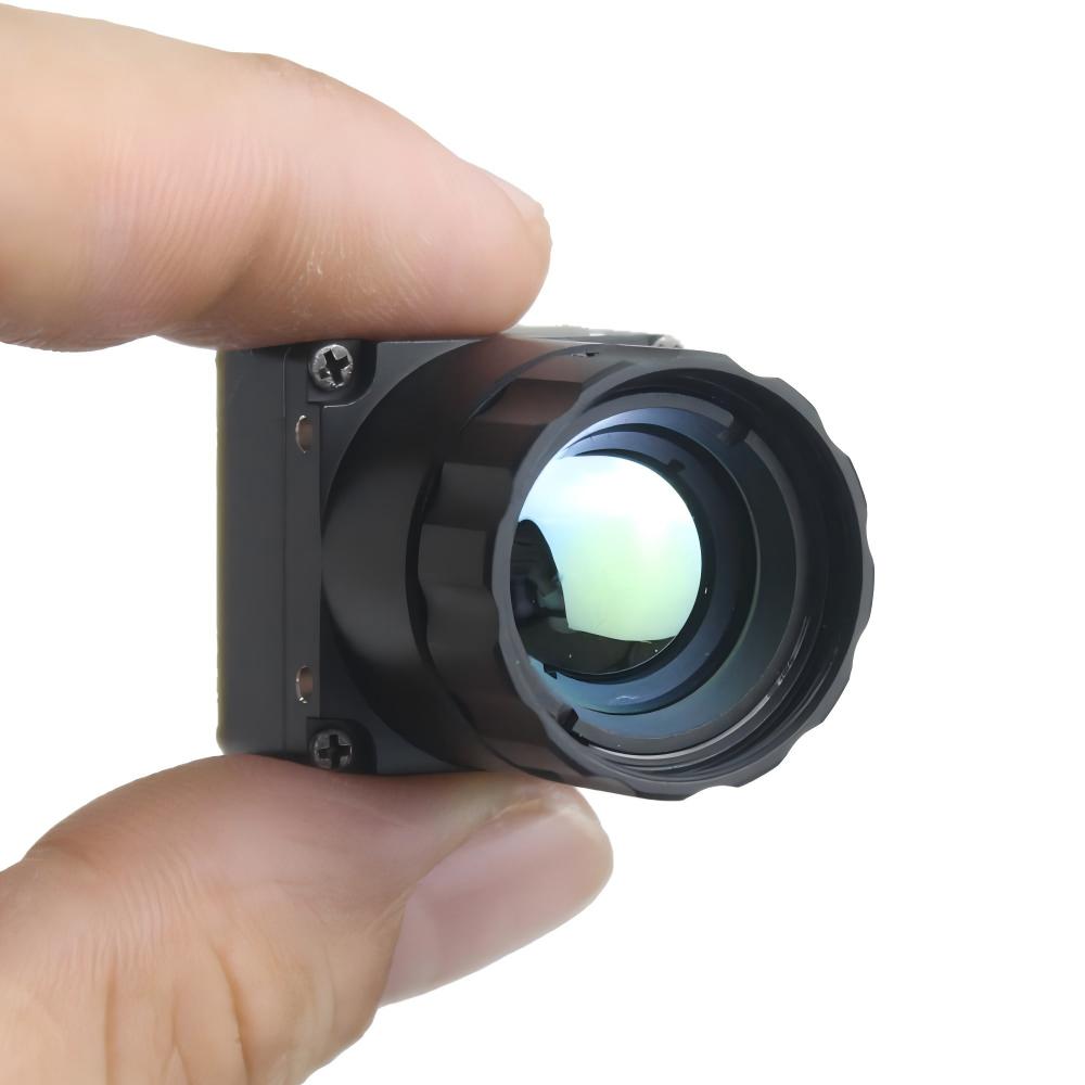
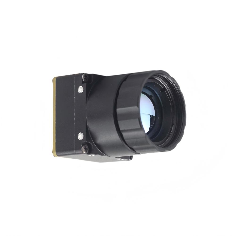
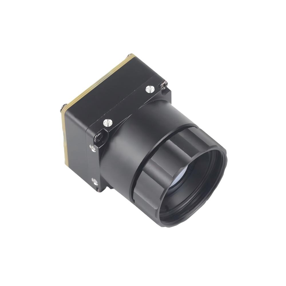
Product Details: Uncooled Infrared Mini 640*512 ASIC Thermal Imaging Camera Module For Drones
| Specification Parameter | Value Details |
|---|---|
| Resolution | 640*512 Pixels |
| Sensor Type | Uncooled VOx Infrared Microbolometer |
| Output Interfaces | RJ45 (RTSP IP), CVBS (Analog Video) |
| Application Suite | Drones, Aerial Gimbals, Industrial Inspection |
| ASIC Processing | Onboard ASIC for real-time AGC, DDE, and 3D DNR |
---
3.2 MD Series 384x288 Integrated Thermal Module
This module is designed for applications where weight and power efficiency are critical, such as small search drones, handheld thermal devices, and compact industrial IoT sensors. It offers MIPI, USB, and CVBS options in a highly compact, lightweight footprint.
MD Series 384x288 uncooled infrared thermal camera module
Product Details: The Purpleriver thermal camera module is designed for industrial-grade precision in applications such as security, temperature monitoring, and drone integration. Featuring an uncooled infrared detector with a 12μm pixel pitch, it delivers high sensitivity and sharp thermal imaging. Its compact size, plug-and-play functionality, and multiple interfaces (MIPI/USB/CVBS) ensure versatile and rapid integration into various systems. Backed by a team with a Hong Kong University of Science and Technology background and former Huawei Hisilicon expertise, this module offers OEM/ODM customization to meet specific project requirements, ensuring unparalleled performance and adaptability.
| Specification Parameter | Value Details |
|---|---|
| Resolution | 384x288 Pixels |
| Pixel Pitch | 12μm |
| Interfaces Supported | MIPI, USB, CVBS |
| Heritage | HKUST & Huawei HiSilicon Sourced R&D Team |
| Customization Types | OEM/ODM Hardware & Software Tailoring |
---
3.3 Architectural Comparison Matrix (Real Hardware Specs)
| Hardware Parameter | Uncooled RJ45 CVBS IP 640 Module | MD Series 384 Uncooled LWIR Module |
|---|---|---|
| FPA Resolution | 640 x 512 pixels | 384 x 288 pixels |
| Pixel Pitch | 12μm | 12μm |
| Thermal Sensitivity (NETD) | ≤ 50mK (F/1.0 at 25°C) | ≤ 40mK (F/1.0 at 25°C) |
| Digital Video Engine | Ethernet IP (H.264/H.265 RTSP) | MIPI-CSI2 / USB 2.0 (UVC Compliant) |
| Analog Video Output | Native CVBS (NTSC/PAL) on dedicated breakout Pins | Native CVBS (NTSC/PAL) via multi-pin header |
| Input Voltage Range | 9.0V to 12.0V DC ± 10% | 3.3V to 5.0V DC ± 5% |
| Power Consumption | Approx. 1.8W to 2.5W (Ethernet active) | Approx. 0.8W to 1.2W (CVBS active) |
| Form Factor / Housing | Fully enclosed metal chassis with bracket mount | Micro open-frame structure with custom adapter plates |
| Optics Interface | Threaded high-performance Germanium Lens | Fixed / Manual Focus Germanium Options |
| Recommended Use Case | Long-range search & rescue drones, security networks | Ultra-lightweight UAV gimbals, Edge AI nodes |
If your system design requires an ultra-lightweight, wide-angle 640-class thermal module without an integrated network port, consider reading the engineering specifications for the Mini 640 Uncooled LWIR Thermal Camera Module.
---
4. Step-by-Step Hardware Integration & UAV Pinout Mapping
Integrating a composite video thermal module into an aerial vehicle or a compact Edge AI enclosure requires precise attention to electrical connections, power filtering, and electromagnetic shielding. Grounding errors here will completely ruin your analog feed.
4.1 Pinout Assignment & Electrical Schematics
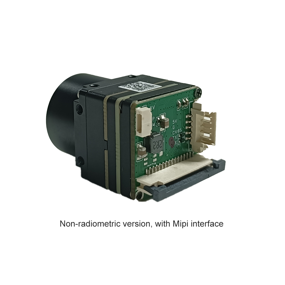
Modern micro-thermal modules utilize fine-pitch connectors (such as 1.0mm JST-SH series) to minimize footprint space. Connecting the core to an analog video transmitter (VTX) or the analog input pins of a flight controller (such as a Pixhawk or Betaflight system) must follow a structured pin configuration:
- ⚙️ VCC (Pin 1): System power input. Ensure the supplied voltage corresponds strictly to the module’s datasheet limits (9V–12V for the 640 IP Core, or 3.3V–5V for the MD Series).
- ⚙️ GND (Pin 2): Common system ground reference. Connect directly to the power distribution board (PDB) ground pad.
- ⚙️ CVBS Out (Pin 3): Unshielded signal line carrying the analog composite baseband signal. This must connect to the video input terminal of your VTX or OSD.
- ⚙️ AGND (Pin 4): Dedicated Analog Video Ground. Always run this ground wire parallel to the CVBS signal line to provide a low-impedance current return loop.
- ⚙️ UART RX/TX (Pins 5 & 6): Logic-level telemetry control interfaces operating at 3.3V TTL thresholds. Connect directly to the host microcontroller’s serial port.
In the shop, we have a golden rule: make sure that Pin 4 (Analog Video Ground) connects directly to the ground pin right next to the video input on your video transmitter (VTX). Do not run this ground through long power distribution paths, or you may introduce significant diagonal lines or scrolling noise into your thermal video stream.
4.2 Eliminating High-Frequency Interference in FPV RF Environments
Standard analog FPV systems operating on 1.2GHz, 2.4GHz, or 5.8GHz bands are highly sensitive to EMI (Electromagnetic Interference) generated by high-power ESCs, brushless motors, and digital processors. High-frequency digital noise can sneak into the analog CVBS lines, degrading the processed thermal image. To prevent this, apply these integration guidelines:
- ✅ Shielded Balanced Lines: Run the CVBS signal and Analog Ground lines together using a twisted-pair wire configuration. For the best signal quality, use low-loss miniature 75-Ohm coaxial cabling (such as RG-178).
- ✅ Faraday Shielding: Enclose all interconnect wiring in an active, braided, tinned-copper shielding sleeve. Ground this jacket at only one end of the run (typically the VTX chassis ground) to prevent ground loops.
- ✅ Keep Distance from High-Power Component Mounts: Secure the sensitive baseband video lines at least 3cm away from high-power, active ESC power cables and high-frequency digital telemetry antennas.
4.3 Power Distribution Network (PDN) and Noise Filtration Designs
Voltage ripple from brushless motors and electronic speed controllers (ESCs) can cause severe horizontal tearing or sync loss on analog video lines. Adding a dedicated LC filter to the power lines prevents this noise from reaching the thermal core. The filter should utilize a high-current 10μH shielded power inductor to block high-frequency current ripples without dropping line voltage.
For smoothing, combine a large 1000μF electrolytic capacitor (to absorb low-frequency voltage sags) with low-ESR ceramic or tantalum capacitors (0.1μF and 470μF, respectively) to suppress high-frequency line noise. Connect all subsystem grounds to a single, central point on the power distribution board to establish a clean star ground reference, keeping high-amplitude motor return currents away from the sensitive analog camera electronics.
---
5. Software Customization & SDK Deployment Guide
While the CVBS output provides immediate real-time video, optimizing thermal sensor settings, shutter calibrations, and measurement palettes requires sending serial commands over the built-in UART interface.
5.1 Serial Command Language (TTL/UART/RS-232) Protocol Implementation
Most industrial uncooled thermal cores communicate over a standard asynchronous serial protocol (typically 115200 bps baud rate, 8 data bits, no parity, 1 stop bit). Below is a complete Python implementation showing how to construct, calculate the checksum for, and send serial command sequences to trigger a manual Flat Field Correction (FFC / Shutter Calibration) or switch pseudo-color palettes:
import serial
import time

class ThermalCoreController:
    # Frame start, command id, length, payload bytes, checksum, frame end
    FRAME_HEADER = 0xAA
    FRAME_FOOTER = 0x55

    def __init__(self, port='/dev/ttyAMA0', baudrate=115200):
        self.ser = serial.Serial(
            port=port,
            baudrate=baudrate,
            bytesize=serial.EIGHTBITS,
            parity=serial.PARITY_NONE,
            stopbits=serial.STOPBITS_ONE,
            timeout=1.0
        )
        print(f"Initialized communication on {port} at {baudrate} bps.")

    def _calculate_checksum(self, packet: bytes) -> int:
        """
        Calculates an 8-bit modular checksum over the raw packet payload
        excluding the header, footer, and the checksum byte itself.
        """
        return sum(packet) & 0xFF

    def _send_command(self, cmd_id: int, payload: list) -> bool:
        length = len(payload)
        # Assemble package payload
        body = [cmd_id, length] + payload
        checksum = self._calculate_checksum(bytes(body))

        # Complete serial packet construction
        full_packet = [self.FRAME_HEADER] + body + [checksum, self.FRAME_FOOTER]
        packet_bytes = bytes(full_packet)

        # Write array directly to the active interface
        self.ser.write(packet_bytes)
        self.ser.flush()
        print(f"Sent Packet: {packet_bytes.hex().upper()}")

        # Read response packet back
        response = self.ser.read(6) # Expecting baseline response frame
        if response:
            print(f"Received Response: {response.hex().upper()}")
            return True
        return False

    def trigger_ffc_shutter(self):
        """
        Triggers a manual flat field correction (FFC) to recalibrate
        and eliminate thermal drift.
        """
        print("Triggering Flat Field Calibration Shutter Switch...")
        # Command 0x0C is standard for NUC/FFC trigger
        return self._send_command(cmd_id=0x0C, payload=[0x01])

    def set_palette(self, palette_idx: int):
        """
        Selects active output pseudo-color palette.
        0x00: White-Hot, 0x01: Black-Hot, 0x02: Ironbow, 0x03: Rainbow
        """
        print(f"Switching Thermal Palette index to: {palette_idx}")
        # Command 0x1F sets pseudo-color
        return self._send_command(cmd_id=0x1F, payload=[palette_idx])

    def close(self):
        self.ser.close()

# Example execution loop
if __name__ == "__main__":
    controller = ThermalCoreController()
    try:
        # Trigger Shutter NUC Calibration
        controller.trigger_ffc_shutter()
        time.sleep(2)
        # Switch output video profile to Black-Hot palette
        controller.set_palette(0x01)
    finally:
        controller.close()
5.2 Edge AI Inference Pipelines: Merging CVBS and Digital Streams
In advanced setups, we run a dual processing pipeline: using the low-latency CVBS analog channel for manual operation (like remote pilot navigation), while routing the high-fidelity digital stream (like USB or MIPI) to an Edge AI companion card (such as a Jetson Orin Nano) for real-time object detection and tracking.
First, the system captures raw frames from the digital stream and rescales them to match the input layer of the target neural network (such as 640 x 640 pixels). Next, the deep learning weights of your object detection library (e.g., YOLOv8-OBB) are quantized from raw floating-point 32-bit (FP32) to highly efficient INT8 precision using TensorRT, maximizing processing speeds on edge-optimized hardware.
Finally, the model analyzes the incoming digital stream, identifying and drawing bounding boxes around high-contrast thermal signatures in real time. Because the analog and digital streams are processed concurrently from the same sensor plane, target coordinates can be fed back to telemetry systems without causing the pilot’s CVBS navigation screen to stutter or drop frames.
---
Mini 640×512 Thermal Imaging Core Demo Video
6. Deep-Dive Engineered FAQ on CVBS & High-Definition Thermal Integration
Can I connect a high-definition infrared thermal module directly to an analog FPV video transmitter (VTX) via CVBS?
How do I get high-definition thermal imaging (640x512) over a CVBS interface without losing detail?
Are these Chinese thermal cores reliable for custom DIY drone and tactical integration?
---
📚 References & Further Reading
- Industry Standard Optics: For custom optical arrays and advanced multi-spectral Germanium lenses, visit Jinde (atmoptics.com).
- Edge Prototyping Hardware: For open-source hardware controllers, sensor breakouts, and edge computing dev kits, browse the resource libraries available on DFRobot.
- Related Guide: Unsure how to budget your payload project? Read our Thermal Camera Module Price Guide (2024).