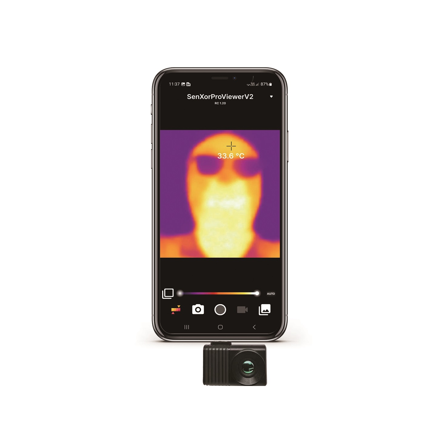
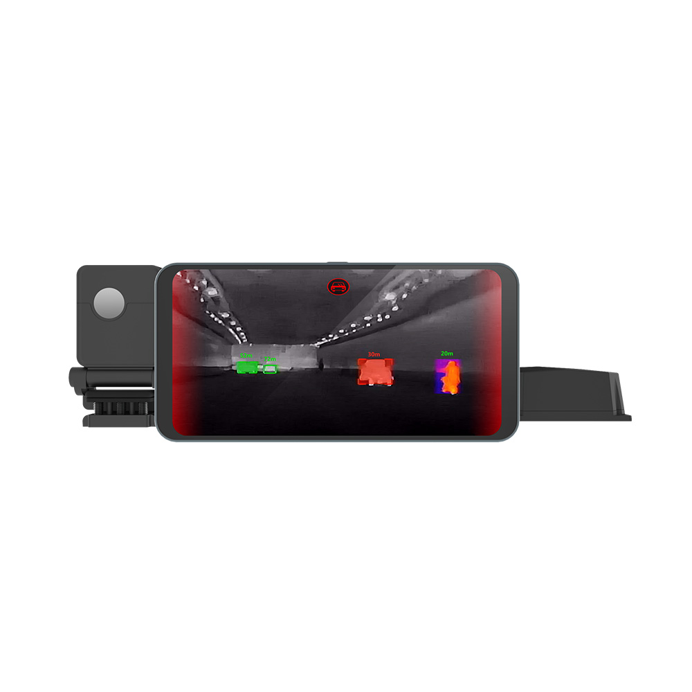


Thermal Camera Module Manufacturer: High-Res Uncooled LWIR Cores for OEM & Embedded Vision
2026年9月3日
Thermal Camera Core OEM: High-Resolution LWIR Modules for Drones & Vision Systems
2026年9月4日
Custom Thermal Camera Module: OEM/ODM IR Cores for Drones, Scopes & Embedded AI
Modern optoelectronic systems demand uncompromised spatial resolution, ultra-low latency, and strict adherence to SWaP-C (Size, Weight, Power, and Cost) constraints. When you are engineering an autonomous unmanned aerial system (UAS), a heavy-recoil thermal weapon sight (TWS), or a smart industrial machine vision line, you learn fast that off-the-shelf thermal imagers simply will not cut it. Designing with a custom thermal camera module gives hardware engineers, embedded architects, and OEM product designers the granular register-level control, custom optical versatility, and board-level routing freedom required to lock down rock-solid deterministic performance in brutal field environments.
Here's the deal: moving from bare focal plane arrays (FPAs) to full-scale deployable hardware is a massive leap. High-density wafer-level packaged (WLP) Vanadium Oxide (VOx) detectors have to interface cleanly with custom Field-Programmable Gate Array (FPGA) logic and Application-Specific Integrated Circuit (ASIC) image processing pipelines. Whether you need to pump uncompressed 14-bit radiometric telemetry into an edge AI accelerator or trim payload mass down to build a sub-20-gram stabilized gimbal, your starting architectural foundation makes or breaks your signal-to-noise ratio (SNR), thermal sensitivity, and host computing budget.
Table of Contents
- 👉 1. Thermal Core Architecture: Microbolometer Arrays & SWaP-C Dynamics
- 👉 2. Hardware Interfaces & Signal Integrity: MIPI-CSI2, USB UVC, and CVBS
- 👉 3. Radiometric Image Processing Pipeline (ISP) & Embedded Edge AI
- 👉 4. OEM/ODM Thermal Camera Modules: Technical Specifications & Comparison
- 👉 5. Integration Playbook: Integrating Thermal Cores into Drones, Scopes, and Handhelds
- 👉 6. Frequently Asked Questions (FAQ)
- 👉 7. Architectural Summary: The Custom Advantage
1. Thermal Core Architecture: Microbolometer Arrays & SWaP-C Dynamics
At the mechanical and silicon core of any modern thermal camera module sits the uncooled microbolometer focal plane array. Operating across the Long-Wave Infrared (LWIR) band between 8 µm and 14 µm, these optoelectronic transducers absorb incident electromagnetic energy radiating from anything warmer than absolute zero. That incoming photonic flux heats up a microscopic, thermally isolated bolometer bridge membrane suspended above the substrate, changing its bulk electrical resistance. Directly below the pixel matrix, a monolithic Readout Integrated Circuit (ROIC) continuously scans these micro-ohmic variations, digitizing sub-millivolt swings into wide-dynamic-range raw digital counts through high-precision onboard 14-bit or 16-bit Analog-to-Digital Converters (ADCs).
When you are trying to squeeze every milliwatt and gram out of a design, you cannot treat the sensor like a generic black box. You have to understand the thin-film physics, package thermals, and mechanical constraints driving the core hardware.

VOx vs. a-Si Thin-Film Physics and Noise Floor Mechanics
Look, the first design crossroad you hit in infrared engineering is the material composition of the MEMS bridge itself: Vanadium Oxide (VOx) versus Amorphous Silicon (a-Si). In the early days of micro-electro-mechanical systems, Amorphous Silicon caught on because fabs could run it right down standard CMOS lines without cross-contaminating equipment. But out in the field, when you are designing high-performance tactical, industrial, or radiometric systems, VOx has won the technical argument hands down.
The root difference boils down to the material's Temperature Coefficient of Resistance (TCR) and its underlying 1/f flicker noise profile. Vanadium Oxide consistently turns in a TCR between -2% and -3% per Kelvin at room temperature (300 K), beating out standard a-Si formulations by a healthy margin. Because signal voltage response scales directly with TCR, a VOx bridge delivers distinctly higher signal output for the exact same thermal flux perturbation. Even better, VOx exhibits lower bulk 1/f noise across low-frequency bias states, which drops your system Noise Equivalent Temperature Difference (NETD) right through the floor.
On the test bench and out in active deployments, high-tier VOx cores reliably pull in sensitivity ratings of ≤40 mK to ≤50 mK at f/1.0. That gives human operators and edge neural nets the ability to detect tiny, sub-fractional thermal differences through atmospheric moisture and obscurants. To see how these noise floor thresholds hold up under field attenuation, check out our comprehensive guide to 50mK NETD thermal modules and high-sensitivity OEM cores.
The 12µm Pixel Pitch Revolution: Optical and Aerodynamic Scaling
Over the last decade, microbolometer lithography has made the jump from legacy 25µm and 17µm dies down to dense 12µm pixel pitches. In the shop, we do not just view this as an incremental lithography upgrade. Shrinking pixel pitch changes the math for the entire mechanical and optical train, kicking off major SWaP improvements across the entire payload:
- ✅ Germanium Glass Reduction: Optical magnification and Field of View (FOV) depend entirely on pixel pitch and focal length ($f$). When you step down from 17µm to 12µm, you can achieve the exact same spatial resolution and angular coverage with a lens that is roughly 29% shorter. Because the aperture diameter scales down to maintain your f-number, the physical volume and mass of the front Germanium (Ge) or Chalcogenide glass drop by 40% to 50%. That cuts raw optical material mass and knocks down overall Bill of Materials (BOM) costs significantly.
- ✅ Wafer-Level Packaging (WLP) Advantages: Older microbolometers sat inside massive metal-canned vacuum packages with heavy ceramic feedthroughs. Contemporary 12µm cores run on Wafer-Level Packaging, where an antireflective silicon or Germanium cap wafer etched with micro-cavities is bonded straight to the sensor wafer under hard vacuum using integrated getter materials. That leaves you with bare-die packages measuring just millimeters per side, pushing bare-board engine weights down below 15 to 20 grams.
- ✅ Fast Stabilization and Lower Battery Draw: A smaller sensor array footprint brings far lower thermal mass. That means modern TEC-less (Thermoelectric Cooler-less) engines reach operational thermal equilibrium in seconds. Smart compensation logic tracks the microbolometer substrate temp via integrated on-chip thermistors, recalculating drift tables on the fly without chewing through battery capacity running active Peltier coolers. Total power consumption comfortably drops to 1.0W–1.2W, which is pure gold for micro-UAS flight longevity.
2. Hardware Interfaces & Signal Integrity: MIPI-CSI2, USB UVC, and CVBS
Getting clean infrared telemetry off an uncooled readout engine and into your host processor means balancing raw bandwidth, pipeline latency, board space, and electromagnetic interference (EMI). A properly designed OEM core has to give you options across its physical layer (PHY), whether you are piping data straight to a high-speed embedded System-on-Chip (SoC) or feeding a zero-latency analog downlink on an agile aircraft.
MIPI CSI-2: Deterministic Low-Latency Bus for Edge AI
When you need high data throughput and sub-frame latency on modern embedded silicon—think NVIDIA Jetson Orin Nano/AGX, Rockchip RK3588, or Raspberry Pi Compute Module 4 (CM4)—MIPI CSI-2 is the undisputed workhorse. Running across a unidirectional D-PHY layer with differential clock lines and scalable data lanes, MIPI CSI-2 dumps raw frame data directly into the host processor's hardware Image Signal Processor (ISP) or direct memory access (DMA) buffers.
By cutting out the protocol translation layers, packet framing, and host-controller buffering delays typical of USB hubs, MIPI gives you deterministic glass-to-glass latency under 5 milliseconds. That is essential when building tight closed-loop applications like autonomous collision avoidance, counter-UAS tracking turrets, or fast-cycling industrial pick-and-place arms. That said, routing high-speed MIPI signals at hundreds of megabits per second requires clean PCB hygiene. You need tightly matched 100-ohm differential impedance microstrip or stripline routing, keeping intra-pair skew under 0.15 mm so you don't crush your eye diagrams. If your signals have to route through a rotating slip ring or modular payload bay, running through micro-coaxial harnesses from industrial connector makers like Amphenol prevents EMI dropouts and high-frequency clock radiation.
USB UVC: Plug-and-Play Architecture for Industrial PCs and Rapid Prototyping
If your end product targets x86 industrial PCs, diagnostic benches, or Linux automation controllers, Universal Video Class (UVC) over USB (USB 2.0 High-Speed or Type-C USB 3.0) gives you the quickest, cleanest bring-up cycle. Because it runs on top of native OS video stacks, you can bring an engine up without wrestling with out-of-tree kernel patches or custom device-tree overlays.
Well-engineered OEM cores present themselves over the USB bus as composite devices. Endpoint 1 runs an isochronous or bulk video stream, delivering uncompressed YUV or pseudocolor RGB at 25 Hz or 50 Hz for direct operator displays. Concurrently, Endpoint 2 opens up a virtual COM port (CDC-ACM) or bulk transfer channel for bidirectional telemetry and control. Through this secondary pipe, your software can trigger Non-Uniformity Correction (NUC) cycles, switch color palettes, feed range-to-target values, or stream frame-synchronized 14-bit linear temperature arrays right alongside the visual feed. During prototype runs, pairing your sensor with carrier systems from modular boards like Waveshare lets your firmware developers hammer out control code long before custom carrier PCBs come back from fab.
CVBS (Composite Video Blanking and Sync): Legacy Zero-Latency FPV Systems
Even with digital networks running everywhere, analog Composite Video Blanking and Sync (CVBS, outputting PAL or NTSC) remains a vital link on tactical First-Person View (FPV) frames and rapid-deployment airframes. The reason comes down to basic communication physics and time-domain performance:
- ✅ Instant Analog Serialization: Modern digital video pipelines (H.264/H.265) need to slice, encode, packetize, and buffer frames, easily tacking on 30 ms to 100 ms of latency. A CVBS feed bypasses all of that, pushing an analog 75-ohm raster line-by-line straight off the core's video DAC. The latency drops below 1 ms, giving FPV pilots instantaneous visual feedback when maneuvering high-speed drones through dense tree canopy or tight urban corridors.
- ✅ Graceful RF Degradation: When a digital wireless feed gets hit with multipath interference or aggressive jamming, it runs into the "digital cliff"—frames freeze, artifacts tear across the screen, and the link drops out completely. Analog video over 5.8 GHz or 1.2 GHz transmitters degrades progressively into visual static. The screen might get noisy, but the pilot can still read the horizon line and steer the airframe home safely.
3. Radiometric Image Processing Pipeline (ISP) & Embedded Edge AI
You cannot just take the raw output of an uncooled microbolometer array and pipe it into a neural network or a display. Because of manufacturing tolerances across more than a hundred thousand microbolometer bridges, every individual pixel comes off the wafer with its own unique DC voltage offset, gain response, and thermal drift profile. Transforming that raw 14-bit data stream into a crystal-clear image while calculating spot-on radiometric temperatures requires an onboard Image Signal Processor (ISP) capable of sustained processing power at full frame rates.
The Real-Time Correction Engine: NUC, BPR, and Spatial Filtering
Before spatial features can be recognized by an operator or model, the camera's FPGA or specialized Vision Processing Unit (VPU) processes the signal through several hardware-accelerated correction stages:
- ⚙️ Non-Uniformity Correction (NUC): Fixed-Pattern Noise (FPN) is the enemy of thermal resolution. The core runs a two-point arithmetic correction pass across every pixel:
$$\text{Corrected\_Pixel}(i, j) = G(i, j) \times \text{Raw\_Pixel}(i, j) + O(i, j)$$
Because the microbolometer substrate drifts along with the internal enclosure temperature, standard modules actuate an internal electromechanical shutter for a fraction of a second to present a uniform blackbody surface and update the offset map $O(i, j)$. In covert tactical operations where you cannot afford an audible shutter click or a frozen frame, advanced cores run scene-based non-uniformity correction (SBNUC) algorithms that dynamically estimate and wipe out spatial drift using moving background data. - ⚙️ Bad Pixel Replacement (BPR): In any microbolometer run, a handful of pixels will be dead, open-circuit, or plagued by random telegraph noise. The BPR block continuously checks incoming pixel coordinates against a factory defect map stored in flash, replacing bad data on the fly using a 3x3 median interpolation of adjacent working cells.
- ⚙️ Temporal and Spatial Filtering (3D-DNR): To pull spatial details out of the noise floor, the processing core applies recursive temporal and bilateral spatial filtering. The temporal filter averages out Gaussian white thermal noise across sequential frames without causing ghosting on fast moving objects, while the bilateral filter strips high-frequency background noise while keeping edge boundaries razor sharp.
If you are integrating these processing pipelines with edge compute architectures for defense platforms, take a look at our practical guide to uncooled VOx Edge AI OEM thermal modules.
Dynamic Range Compression: Digital Detail Enhancement (DDE) vs. Linear Radiometry
A native 14-bit thermal stream gives you 16,384 distinct digital energy values. The problem is that standard visual microdisplays and displays only render an 8-bit signal (256 grayscale levels). If you simply map that 14-bit signal linearly down to 8 bits, low-contrast human targets or vehicle signatures blend completely into the background, particularly in scenes with wide thermal extremes.
To fix this, modern thermal ISPs run Digital Detail Enhancement (DDE). The pipeline splits the high-dynamic-range image into two streams: a low-frequency base layer (the overall scene background and broad dynamic temperature shifts) and a high-frequency detail layer (fine textures, small temperature gradients, and target silhouettes). The detail layer is amplified using Contrast-Limited Adaptive Histogram Equalization (CLAHE) and dynamically recombined with the compressed base layer. The final 8-bit image pops, bringing out hidden foliage details, subtle terrain changes, and faint footprints.
On the flip side, when you are building predictive maintenance cameras or fire-spotting platforms, pretty pictures take a back seat to absolute temperature values. Radiometric engines bypass dynamic tone mapping and apply Planck calibration curves alongside real-time parameters: emissivity ($\epsilon$), ambient reflected temperature ($T_{\text{refl}}$), distance, and atmospheric humidity. The output transforms into a T-Linear matrix where each digital count represents an exact temperature value (for example, a digital number of 2540 corresponds to exactly 25.40°C).
For more architectural insights on tailoring uncooled cores for harsh border and perimeter operations, check our technical breakdown of uncooled OEM thermal cores.
4. OEM/ODM Thermal Camera Modules: Technical Specifications & Comparison
Selecting an OEM thermal engine comes down to matching your physical envelope, optical train, and software interfaces against field-proven hardware. Designed by an engineering team drawing on talent from the Hong Kong University of Science and Technology (HKUST) and former Huawei HiSilicon silicon specialists, the two modules below represent battle-tested solutions for airborne gimbals, tactical optics, and embedded computer vision pipelines.
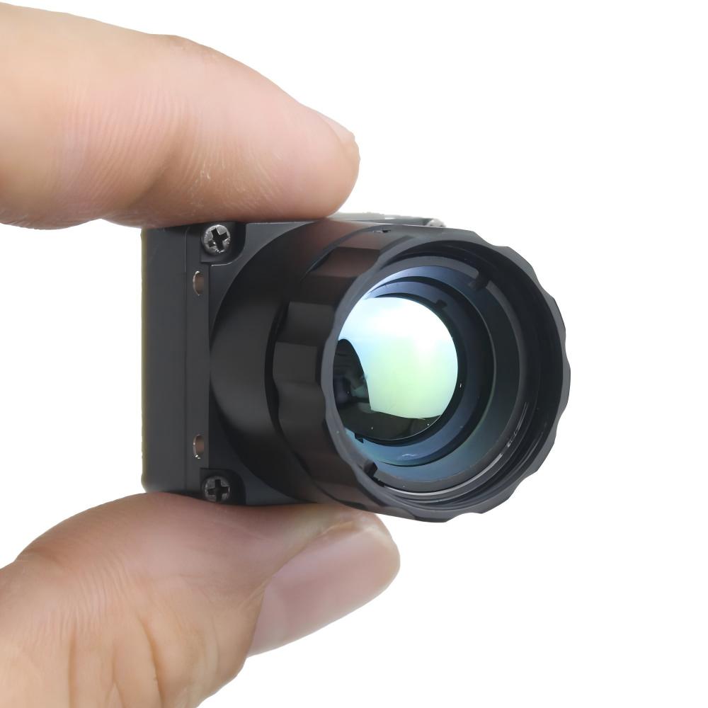
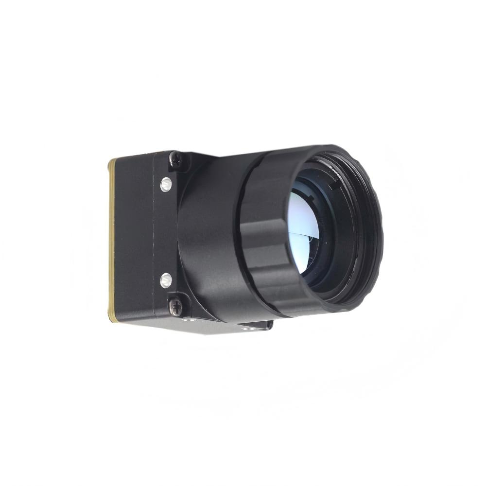
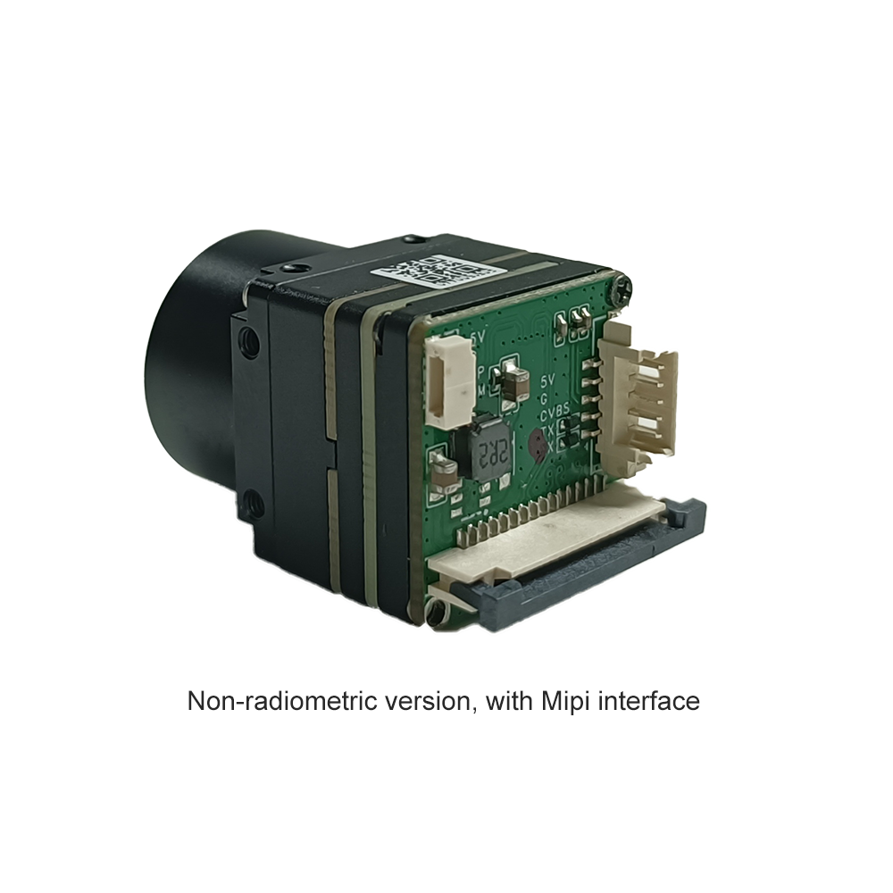
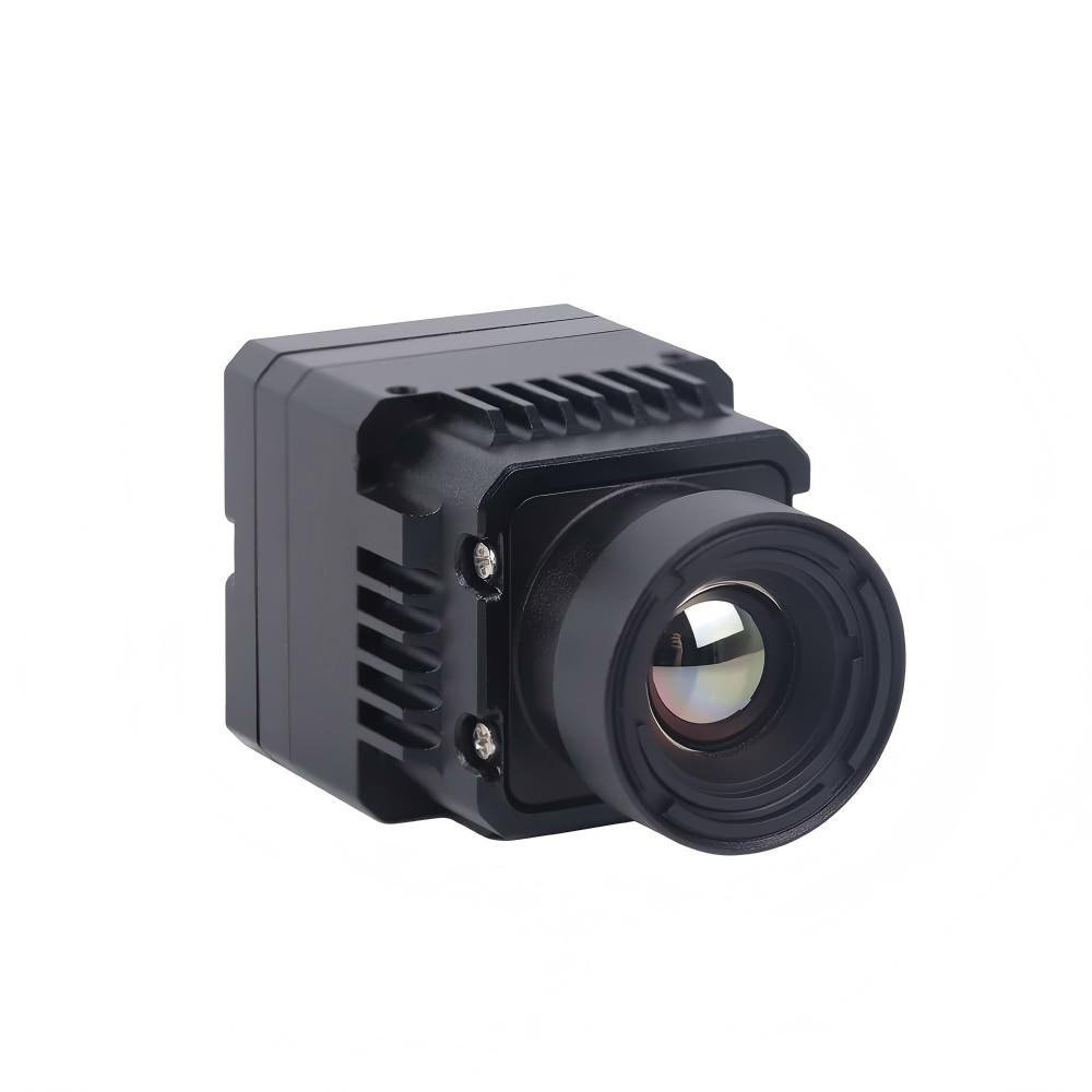
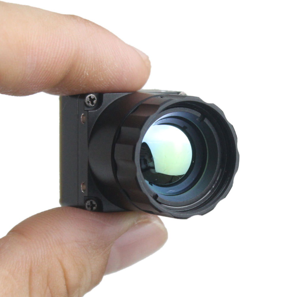
Uncooled Mini 384*288 Thermal Camera Module For Drones
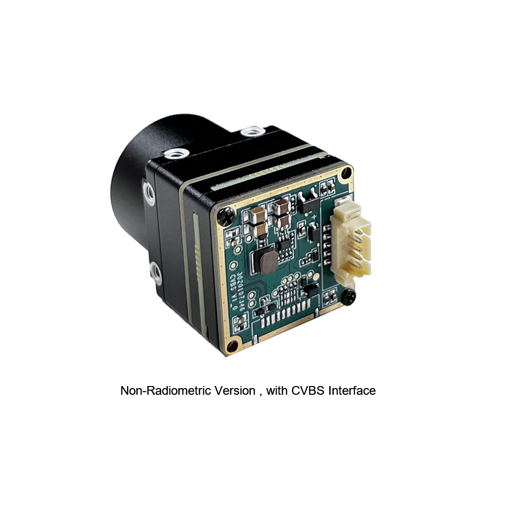
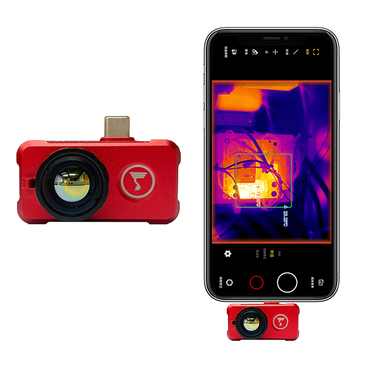
The MINI series infrared thermal imaging temperature measurement module is a high-precision, small-sized, and universal online temperature measurement infrared thermal imager. It uses high-quality detectors, high resolution, stable performance, and powerful functions. It is equipped with multiple interfaces, making it a preferred product in application fields such as machine vision, safety inspection, intelligent manufacturing, equipment maintenance, robot drone airborne, and so on.
- ✅ Optimized Airborne SWaP: Ultra-miniature footprint designed explicitly to preserve drone battery capacity and fit within compact mechanical gimbals.
- ✅ Radiometric Precision: Supports industrial online temperature measurement with full-frame spot, line, and area temperature telemetry.
- ✅ Broad Deployment Scope: Seamlessly matches robotic autonomous navigation, airborne power-line inspection, and search-and-rescue.
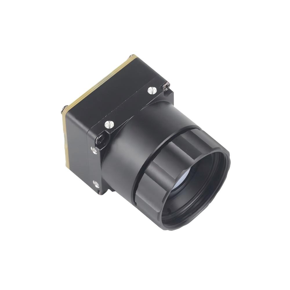
MD Series 384x288 Uncooled Infrared Thermal Camera Module
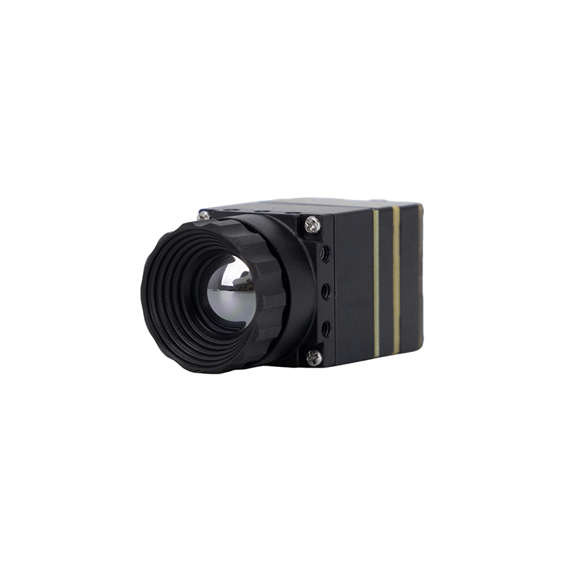
The Purpleriver thermal camera module is designed for industrial-grade precision in applications such as security, temperature monitoring, and drone integration. Featuring an uncooled infrared detector with a 12μm pixel pitch, it delivers high sensitivity and sharp thermal imaging. Its compact size, plug-and-play functionality, and multiple interfaces (MIPI/USB/CVBS) ensure versatile and rapid integration into various systems. Backed by a team with a Hong Kong University of Science and Technology background and former Huawei Hisilicon expertise, this module offers OEM/ODM customization to meet specific project requirements, ensuring unparalleled performance and adaptability.
- ✅ Multi-Interface Versatility: Native tri-interface support delivering MIPI-CSI2, USB (UVC), and CVBS concurrent output.
- ✅ 12µm Pixel Pitch Architecture: High-density VOx FPA maximizing optical DRI while reducing front-element Germanium mass.
- ✅ OEM/ODM Customization: Custom flex cables, lens mounts, firmware registers, and thermal calibration look-up tables.
Direct Engineering Specification Matrix
| Engineering Metric | Uncooled Mini 384*288 Module | MD Series 384x288 Module |
|---|---|---|
| Detector Architecture | Uncooled VOx Microbolometer | Uncooled VOx Microbolometer |
| Array Resolution | 384 × 288 Pixels | 384 × 288 Pixels |
| Pixel Pitch | 12 μm | 12 μm |
| Spectral Band | 8 μm ~ 14 μm (LWIR) | 8 μm ~ 14 μm (LWIR) |
| Frame Rate | 25 Hz / 50 Hz | 25 Hz / 50 Hz |
| Thermal Sensitivity (NETD) | ≤40 mK to ≤50 mK @ f/1.0, 300K | ≤40 mK to ≤50 mK @ f/1.0, 300K |
| Hardware Interfaces | CVBS (Analog), Digital Output Bus | MIPI-CSI2, USB (UVC), CVBS |
| Radiometric Modes | Online Spot, Line, Area Temp Analysis | Full Radiometric 14-bit Stream & Video |
| Typical Power Draw | < 1.0 W (Optimized low-draw state) | < 1.2 W (Multi-interface streaming) |
| Lens Interfacing | Fixed Focus / Athermalized M10/M12 | M10, M12, Custom Manual/Motorized |
5. Integration Playbook: Integrating Thermal Cores into Drones, Scopes, and Handhelds
Taking an OEM core off the bench and getting it ready for the real world is where the rubber meets the road. Vibration, thermal cycling, and RF noise can ruin an integration if you have not addressed the physical boundary conditions.
1. Airborne UAS Payloads and Micro-Gimbals
When you are packaging thermal cores into 2-axis or 3-axis brushless gimbals, mass distribution matters just as much as overall weight. The center of gravity (CoG) of your optical block and module has to line up directly on the intersection of your pitch and roll axes. If you are off by even half a millimeter, the brushless motors are constantly fighting counter-torque, driving up current draw, creating high-frequency micro-jitter in the IMU, and cutting flight time.
Rigid coaxial bundles will fight motor movement across gimbal joints. You need to run custom Flexible Printed Circuits (FPC) with polyimide layers and etched routing channels. These flex harnesses need deliberate service loops calculated around bend radii to survive hundreds of thousands of duty cycles without trace cracking. Keep your EMI shielding tight: a bare microbolometer clock circuit will pick up radiation from nearby 915 MHz/2.4 GHz telemetry transmitters or 5.8 GHz video gear. Wrap the module inside an anodized aluminum enclosure bonded directly to system ground to keep clock jitter out of the video feed.
2. Thermal Weapon Sights (TWS) and Extreme Shock Environments
Weapon optics face mechanical shocks that would destroy ordinary industrial electronics. Mount an optic on a rifle platform chambered in .308 Winchester or a 12-gauge shotgun, and the electronics see instantaneous shock loads between 500G and 1200G in under a millisecond. If you do not plan for that mechanical spike, you will face delaminated dies, optical shifts, or sheared solder joints.
- ⚙️ Mechanical Standoffs and Conformal Potting: Never rely on friction-fit board headers inside a scope. Every PCB layer must be secured with multi-point stainless or brass standoffs, and large surface-mount ICs, inductors, and connectors need structural underfill or potting to stop solder joints from fatiguing under recoil.
- ⚙️ FPGA-Driven Reticle Hardware Overlays: In the field, you cannot trust software-rendered reticles driven by an operating system frame buffer; a Linux kernel hiccup could freeze your crosshair while the target moves. Advanced cores burn ballistic reticle overlays directly into the hardware display path inside the on-core FPGA. That gives you zero-latency reticle positioning with zero risk of software lag.
- ⚙️ Optomechanical Athermalization: Tactical sights operate from -40°C in freezing conditions up to +60°C in intense desert heat. Standard metal lens barrels expand and contract with temperature swings, throwing off focus. You need athermalized optical designs that combine positive and negative lens elements mounted inside alternating sleeves of aluminum and Delrin to keep focus locked at infinity across the entire operating temp envelope.
3. Embedded Industrial Automation & Condition Monitoring
In fixed factory deployments—like continuous battery cell inspection lines, switchgear cabinets, or chemical processing plants—modules run 24/7 inside sealed, fanless IP66 or IP67 housings. The engineering challenge shifts from managing mechanical shock to dissipating heat passively.
In a sealed box, that 1.0W of heat from the ISP can raise the internal temperature past the module's +70°C ceiling if it has nowhere to go. You have to design a solid thermal path from day one. Machine an aluminum thermal bridge that mates the module's rear ground plane to the outer enclosure, using compressible gap pads rated for at least 3.0 to 5.0 W/m-K.
From there, your embedded host processor can ingest clean 14-bit T-linear data over MIPI or USB, routing frames directly into edge models like YOLOv8 or TensorRT pipelines on an industrial Jetson board. This lets the system flag thermal anomalies and bearing wear milliseconds before an industrial machine experiences catastrophic failure.

6. Frequently Asked Questions (FAQ)
How do I stream real-time raw/radiometric thermal video directly to a Raspberry Pi or custom embedded SBC?
Can these thermal modules be customized for ultralight drone gimbals and DIY thermal optics?
What is the key advantage of an industrial OEM thermal core over hobbyist sensors like MLX90640 or entry-level modules?
7. Architectural Summary: The Custom Advantage
Getting a high-performance thermal imager into production is a balancing act of optical physics, analog noise management, high-speed digital buses, and low-latency image processing. Off-the-shelf consumer thermal units inevitably force compromises on board layout, interface options, or temperature measurement reliability. By building on an industrial-grade, fully customizable OEM/ODM thermal engine, you bypass years of low-level optoelectronic debugging and jump straight to field-ready payloads.
Whether your roadmap calls for an FPV drone engine running zero-latency analog CVBS, an autonomous aerial platform demanding sub-40mK sensitivity over MIPI, or a smart factory radiometry sensor, Purpleriver's engineering team—combining research out of the Hong Kong University of Science and Technology with former Huawei HiSilicon silicon experience—delivers the hardware reliability and design flexibility you need to build mission-ready gear.
📚 References & Further Reading
- Industry Standard: High-speed industrial interconnect solutions and signal integrity guidelines via Amphenol
- Industry Standard: Embedded developer hardware and modular evaluation ecosystems by Waveshare
- Related Guide: Best 50mK NETD Thermal Module Guide: OEM Cores for High Sensitivity
- Related Guide: Przewodnik Zakupu Niechłodzonego Modułu Termowizyjnego VOx Edge AI OEM
- Related Guide: وحدات الكاميرا الحرارية غير الإشعاعية: دليل المهندس للأجهزة المدمجة