

Thermal Camera Guide: How It Works, Value Analysis, and OEM Module Integration
2026年10月14日
Thermal Camera Guide: How to Choose, Integrate, and Maximize AI Infrared Performance
2026年10月16日
Thermal Imaging Camera Guide: Real-World Testing, Resolution & OEM Cores
Thermal imaging has transformed from a classified defense technology into an essential pillar of industrial metrology, predictive maintenance, automated process control, and autonomous aerial robotics. Whether an engineer is isolating a 0.5-milliwatt parasitic leakage across a sub-millimeter surface-mount capacitor on an active multi-layer printed circuit board (PCB) or integrating an uncooled sensor payload into an unmanned aerial vehicle (UAV) for standoff reconnaissance, selecting the ideal thermal imaging camera core requires navigating complex engineering specifications. System-level radiometric performance is dictated by unalterable optical physics, semiconductor solid-state mechanics, sensor thermal time constants, and algorithm-driven digital signal processing pipelines.
Procurement specialists, embedded systems architects, and field diagnostic engineers routinely confront challenging design trade-offs. Balancing spatial resolution, Noise Equivalent Temperature Difference (NETD), frame rate latency, optic transmission curves, and Size, Weight, Power, and Cost (SWaP-C) constraints demands a fundamental understanding of sensor design. This guide provides an in-depth technical analysis of uncooled Long-Wave Infrared (LWIR) microbolometers, detailing physical sensor architectures, mathematical calibration frameworks, real-world bench testing protocols, and industrial OEM integration platforms.
Table of Contents
- 👉 1. Physics of Infrared Thermography: LWIR Spectrum & Sensor Architecture
- 👉 2. Microbolometer Core Engineering: VOx vs. a-Si & NETD Sensitivity Realities
- 👉 3. Spatial Resolution, Pixel Pitch, and Lens Optics: 256x192 vs. 640x512
- 👉 4. Benchtop & Field Testing Protocols: Radiometric Calibration, Drift, and NUC
- 👉 5. Embedded Systems Integration: USB, MIPI, and Drone Hardware Interfaces
- 👉 6. Industrial OEM Thermal Camera Cores: Comparative Specification Matrix
- 👉 7. Mission-Critical Deployment: PCB Diagnostics, Aerial Surveillance & Edge AI
- 👉 8. Deep-Dive Engineering FAQ
1. Physics of Infrared Thermography: LWIR Spectrum & Sensor Architecture
Every physical object with a thermodynamic temperature exceeding absolute zero (0 Kelvin or -273.15°C) continuously emits electromagnetic radiation due to the random thermal motion of its constituent atoms and molecules. The spectral characteristics and magnitude of this radiant flux are defined mathematically by fundamental thermodynamic laws. Planck’s Radiation Law expresses the spectral radiance of an idealized blackbody emitter across discrete wavelengths:
B(λ, T) = (2hc² / λ&sup5;) × [1 / (exp(hc / (λk_B T)) - 1)]
where h represents Planck’s constant, c is the speed of light in a vacuum, k_B denotes the Boltzmann constant, λ is the electromagnetic emission wavelength, and T is the absolute temperature in Kelvin. Integrating Planck’s distribution over all radiating wavelengths yields the Stefan-Boltzmann Law, quantifying total hemispherical radiant emittance (j*):
j* = ε σ T&sup4;
Here, ε represents surface emissivity (the efficiency with which a real surface radiates thermal energy relative to an ideal blackbody of identical temperature), and σ is the Stefan-Boltzmann constant (5.670374 × 10&sup8; W·m²·K&sup4;). Furthermore, Wien’s Displacement Law establishes that the peak emission wavelength (λ_max) shifts inversely with temperature according to λ_max = b / T, where b is Wien’s displacement constant (approximately 2897.8 μm·K).
For terrestrial surfaces and industrial targets operating within ambient atmospheric envelopes (-40°C to +150°C, or 233 K to 423 K), peak spectral radiance falls predominantly within the Long-Wave Infrared (LWIR) band, spanning wavelengths between 8.0 μm and 14.0 μm. This spectrum offers two distinct operational advantages for industrial thermography:
- ✅ Atmospheric Transmission Efficiency: The terrestrial atmosphere exhibits extraordinarily low attenuation across the 8.0 μm to 14.0 μm optical window. Unlike the Short-Wave Infrared (SWIR, 1.4 μm to 3.0 μm) or Mid-Wave Infrared (MWIR, 3.0 μm to 5.0 μm) bands, LWIR radiation experiences minimal molecular absorption from atmospheric water vapor (H&sub2;O), carbon dioxide (CO&sub2;), and ozone (O&sub3;) over typical operational standoff distances.
- ✅ Solar Reflection Immunity: Solar radiation consists primarily of visible and short-wave infrared flux, peaking near 0.5 μm and dropping sharply past 3.0 μm. Consequently, daylight reflections off exterior metal structures, solar panels, and outdoor facilities generate negligible direct solar interference within the 8.0 μm to 14.0 μm band, allowing pure self-emission thermography during direct sunlight conditions.
Microbolometer Focal Plane Array (FPA) Architecture
Modern industrial thermal imaging cameras utilize uncooled Focal Plane Array (FPA) microbolometers. Unlike photon-counting detectors found in cryogenically cooled MWIR systems that rely on internal photoelectric excitation, microbolometers are thermomechanical transducers. Each sensor pixel operates on thermal absorption rather than direct photon-to-electron generation.
The structural core of each individual microbolometer pixel consists of an ultra-thin absorbing membrane, measuring between 12 μm and 17 μm on a side. This membrane is suspended roughly 2 μm above an underlying silicon CMOS Readout Integrated Circuit (ROIC) via two micro-machined supporting legs. These structural legs serve a dual function: they provide mechanical support and establish the critical electrical contact pathway to the ROIC while maintaining a strictly engineered thermal conductance path. To maximize absorption of incoming LWIR photons, the cavity depth beneath the suspended membrane is configured as a quarter-wave (λ/4) resonant optical cavity, trapping and absorbing incident infrared waves within the active thin film.
Because ambient air molecules facilitate rapid convective and conductive heat exchange that would overwhelm micro-Kelvin temperature shifts, the entire microbolometer array is hermetically encapsulated inside an ultra-high vacuum environment. This packaging is achieved via wafer-level packaging (WLP) using getter materials to absorb residual gas molecules, maintaining deep vacuum over multi-year operational lifespans. When LWIR radiation focused by a germanium lens strikes the micro-bridge, the absorbed energy raises the membrane temperature, altering its internal electrical resistance. The ROIC sequentially measures this resistance change across high-speed row and column multiplexers, converting analog voltage shifts into digital representations of thermal radiance.
2. Microbolometer Core Engineering: VOx vs. a-Si & NETD Sensitivity Realities
The thin-film semiconductor material layered onto the microbolometer membrane directly dictates signal-to-noise ratio (SNR), operational response time, thermal time constants, and calibration stability. The modern uncooled thermal imaging market is dominated by two primary semiconductor thin-film technologies: Vanadium Oxide (VOx) and Amorphous Silicon (a-Si).
| Engineering Metric | Vanadium Oxide (VOx) | Amorphous Silicon (a-Si) |
|---|---|---|
| Temperature Coefficient of Resistance (TCR) | -2.0% to -3.0% / K | -2.5% to -4.0% / K |
| 1/f Low-Frequency Flicker Noise | Exceptionally Low | Elevated (due to dangling bonds) |
| Typical Core NETD Capability | < 30 mK to 50 mK | Typically ~50 mK to 80 mK |
| Thermal Time Constant (τ) | 8 ms to 12 ms (High agility) | 10 ms to 16 ms (Slower frame decay) |
| Long-Term Metrological Drift | Minimal / Highly stable phase state | Moderate / Higher offset drift rates |
A microbolometer's sensitivity is governed by its Temperature Coefficient of Resistance (TCR), defined as:
TCR = (1 / R) × (dR / dT)
While hydrogenated amorphous silicon (a-Si:H) can achieve elevated nominal TCR values in controlled cleanroom settings, it suffers from pronounced 1/f low-frequency flicker noise. This intrinsic noise stems from structural defects, structural disarray, and dangling atomic bonds within its non-crystalline amorphous silicon matrix. When bias currents traverse an a-Si element, these microscopic electron traps generate random fluctuations in resistance that compete directly with the thermal signal.
Conversely, Vanadium Oxide (VOx) represents a multi-phase mixed-valence compound (predominantly VO&sub2; and V&sub2;O&sub5;) exhibiting correlated electron dynamics. It combines a predictable -2% to -3%/K TCR with exceptionally low 1/f flicker noise. This low noise floor yields a significantly superior Signal-to-Noise Ratio (SNR), enabling VOx-based thermal sensors to register faint thermal differentials across scenes with high dynamic range. As a result, VOx serves as the preferred detector material for mission-critical aerial drones, target recognition devices, and high-precision metrological instruments.
Deconstructing NETD: Lab Benchmark vs. Field Reality
Noise Equivalent Temperature Difference (NETD) serves as the primary standardized metric for evaluating thermal sensitivity. Expressed in milli-Kelvin (mK), NETD represents the temperature differential that produces a signal voltage equal to the root-mean-square (RMS) system noise:
NETD = (4 × F² × v_n) / [τ_o × A_det × (dP / dT) × R_v]
where F denotes the optical f-number of the objective lens, v_n represents the integrated electronic and thermal noise voltage, τ_o is the lens transmission coefficient, A_det is the active microbolometer pixel area, dP/dT is the temperature derivative of radiant emittance within the spectral band, and R_v is sensor responsivity. While laboratory datasheets commonly cite NETD figures such as “≤ 40 mK at f/1.0, 300 K,” engineers integrating thermal cameras into real-world systems must account for key environmental variables:
- ⚙️ Optic Aperture Derating: Radiative irradiance landing on the FPA scales inversely with the square of the lens f-number (E ∝ 1/F²). If an engineer replaces a wide, heavy f/1.0 laboratory test optic with an ultra-compact, cost-effective f/1.3 or f/1.4 lens assembly, the thermal energy reaching the sensor is cut roughly in half. An OEM core rated at 40 mK degrades to an effective system-level NETD of 67 mK to 78 mK, reducing its ability to resolve faint thermal anomalies.
- ⚙️ Substrate Temperature Fluctuation: In uncooled, TEC-less (Thermoelectric Cooler-less) camera modules, ambient environmental fluctuations shift the temperature of the internal camera chassis. Without active temperature stabilization, thermal gradients develop across the ROIC substrate, causing baseline signal drift. To prevent degradation of the sensor's native NETD, the core's digital signal processing engine must run dynamic offset tracking algorithms.
3. Spatial Resolution, Pixel Pitch, and Lens Optics: 256x192 vs. 640x512
Selecting the spatial resolution for an uncooled thermal imaging camera requires balancing target size, required standoff distance, data throughput, and physical optical dimensions. The industrial imaging market has largely standardized on two resolution classes: 256 × 192 pixels (49,152 sensing elements) and 640 × 512 pixels (327,680 sensing elements).
| Optical Metric | 256 × 192 (12 μm Pitch) | 640 × 512 (12 μm Pitch) |
|---|---|---|
| Active Sensing Element Count | 49,152 pixels | 327,680 pixels (6.66× data volume) |
| Instantaneous Field of View (IFOV, 9mm Lens) | 1.33 mrad | 1.33 mrad (6.66× wider spatial scene) |
| Uncompressed Data Rate (16-bit, 25 Hz) | ~2.45 MB/s (Low compute overhead) | ~16.38 MB/s (Requires robust DMA/Bus) |
| Target Identification Range (DRI Criteria) | Close-to-Mid Range (0.1 m to 50 m) | Extended Standoff (5 m to 500+ m) |
| Typical Lens Clear Aperture Requirement | Small / Lightweight Germanium | Larger diameter for telephoto ranges |
Optical Calculations: IFOV and Spot Size Ratio
Resolution in infrared thermography dictates geometric spatial sampling and absolute measurement accuracy. Two primary optical principles govern these limits: Instantaneous Field of View (IFOV) and the Measurement Spot Size Ratio (SSR).
IFOV characterizes the single-pixel angular projection onto the target plane:
IFOV = d / f'
where d represents the physical detector pixel pitch (e.g., 12 μm) and f' is the focal length of the objective lens. Multiplying IFOV by the target distance (D) determines the physical dimensions of the optical footprint mapped onto a single pixel. However, engineers cannot base absolute temperature measurements on a single pixel footprint. Due to the optical Modulation Transfer Function (MTF), diffraction blurring, and optical aberrations across Germanium glass elements, a single pixel cannot capture the full radiant amplitude of an isolated target.
To capture accurate temperature data without signal attenuation from adjacent background areas, the target must fully cover an array of at least 3 × 3 continuous pixels. This requirement defines the Measurement Instantaneous Field of View (MFOV), commonly referred to as the Spot Size Ratio (SSR). If an inspection target fails to cover this 3 × 3 pixel window, peripheral background temperatures will bleed into the measurement, leading to significant temperature reading errors.
For close-in benchtop diagnostic work, such as inspecting active surface-mount components on a circuit board, a 256 × 192 sensor with macro optics provides sufficient spatial detail to detect sub-millimeter component failures. Conversely, for high-altitude UAV search missions or industrial perimeter surveillance, a 640 × 512 matrix provides 6.66 times the spatial sampling data, allowing target identification at extended standoff distances.
4. Benchtop & Field Testing Protocols: Radiometric Calibration, Drift, and NUC
An uncalibrated microbolometer cannot measure absolute temperatures out of the box. The raw digital number (DN) reported by each pixel reflects variations in individual detector resistance, silicon doping tolerances, housing thermal emission, and amplifier offsets rather than pure target radiance. To convert raw 14-bit or 16-bit digital counts into calibrated radiometric temperature values, systems use standardized calibration algorithms.
1. Two-Point Non-Uniformity Correction (NUC)
Each individual pixel in a microbolometer array exhibits distinct responsivity and offset characteristics. The two-point NUC process maps these responses to a uniform baseline using two precision Cavity Blackbody reference sources set to known temperatures, T_cold and T_hot:
DN_corrected(i, j) = G(i, j) × [DN_raw(i, j) - Offset(i, j)]
During factory calibration, the camera captures multiple frames at both temperature setpoints. The algorithm calculates the gain coefficient G(i, j) and offset coefficient Offset(i, j) for every pixel across the array. Defective pixels that exhibit dead outputs, excessive thermal drift, or saturated noise floors are mapped out into a static Bad Pixel Map (BPM). At runtime, the image processor interpolates values for these bad pixels from neighboring operational detectors using nearest-neighbor directional filtering.
During active operation, environmental temperature shifts cause the camera chassis to expand and contract, introducing thermal drift. To recalibrate the sensor, an internal electromagnetic solenoid momentarily moves a uniform mechanical shutter in front of the array for roughly 250 milliseconds. This process, known as Flat-Field Correction (FFC), updates the offset coefficients for every pixel, clearing Fixed-Pattern Noise (FPN) and ghosting artifacts from the display.
2. Absolute Temperature Reconstruction
After applying non-uniformity corrections, the system calculates absolute object temperatures using an empirical adaptation of the Planck radiation formula. The software engine compensates for target emissivity, atmospheric attenuation, and ambient reflections:
DN_target = (DN_total - (1 - ε) × τ_atm × DN_refl - (1 - τ_atm) × DN_atm) / (ε × τ_atm)
T_target = B / [ln(R / (DN_target + F))]
where R, B, and F represent factory-calibrated Planck curve parameters stored within the module's non-volatile memory, ε is target surface emissivity, τ_atm is the transmission coefficient across the measurement distance, DN_refl accounts for ambient reflections off the target, and DN_atm represents radiation emitted by the intervening air column. Precise radiometric accuracy requires adjusting these parameters to match current field conditions.
5. Embedded Systems Integration: USB, MIPI, and Drone Hardware Interfaces
Integrating an uncooled thermal camera core into an embedded edge compute platform requires designing across physical, electrical, and data interface layers. System architects must handle high-bandwidth 16-bit sensor streams while keeping total power consumption and heat dissipation to a minimum.
Electrical Interfacing and Protocol Stacks
Thermal camera cores generally support three main electrical interface standards:
- ⚙️ USB 2.0 / USB 3.0 (UVC Class): Modern compact cores often implement the standardized USB Video Class (UVC) protocol. This allows engineers to plug the thermal sensor directly into an embedded Linux host and begin streaming without writing proprietary kernel drivers. Modern cores can stream raw radiometry using the uncompressed 16-bit greyscale (Y16) format, where each pixel value maps directly to an absolute temperature value, or down-sampled 8-bit YUV/RGB frames with pre-applied color palettes for real-time monitoring.
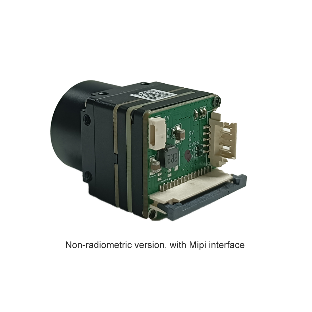
- ⚙️ MIPI-CSI-2 / Parallel DVP: For ultra-low-latency or weight-constrained drone micro-gimbals, bypassing USB bridge chips reduces board space and power consumption. The Mobile Industry Processor Interface (MIPI) Camera Serial Interface 2 (CSI-2) streams raw sensor data directly into the host processor's Image Signal Processing (ISP) pipeline with sub-millisecond latency. High-density, vibration-resistant board-to-board connectors—such as those manufactured by Molex—provide the mechanical stability required in high-vibration drone and mobile robotics applications.
- ⚙️ Single-Board Computer Processing: Embedded platforms such as the Raspberry Pi or NVIDIA Jetson provide versatile platforms for thermal imaging edge computing. System designers can configure Linux Video4Linux2 (V4L2) drivers to capture raw Y16 frames directly into user-space memory, where OpenCV and on-device machine learning models can process the data in real time. For architectural blueprints and setup routines, review our guide on RS300 thermal camera driver configuration, or explore options for high-resolution LWIR streaming modules for Raspberry Pi.
6. Industrial OEM Thermal Camera Cores: Comparative Specification Matrix
When engineering thermal imaging systems for OEM platforms—such as uncrewed mine reconnaissance vehicles, aerial search payloads, or industrial automation setups—miniaturization and radiometric precision are top priorities. Below is an engineering comparison of two industry-proven uncooled LWIR cores.
| Specification Parameter | Uncooled LWIR Mini 256*192 Module | Uncooled LWIR USB Mini 640*512 Module |
|---|---|---|
| Detector Architecture | Uncooled LWIR VOx Microbolometer | Uncooled LWIR VOx Microbolometer |
| FPA Resolution | 256 × 192 (49,152 active pixels) | 640 × 512 / 640 × 480 (327,680 pixels) |
| Spectral Band | 8.0 μm to 14.0 μm (LWIR) | 8.0 μm to 14.0 μm (LWIR) |
| Thermal Sensitivity (NETD) | ≤ 50 mK at f/1.0, 300 K | ≤ 40 mK to 50 mK at f/1.0, 300 K |
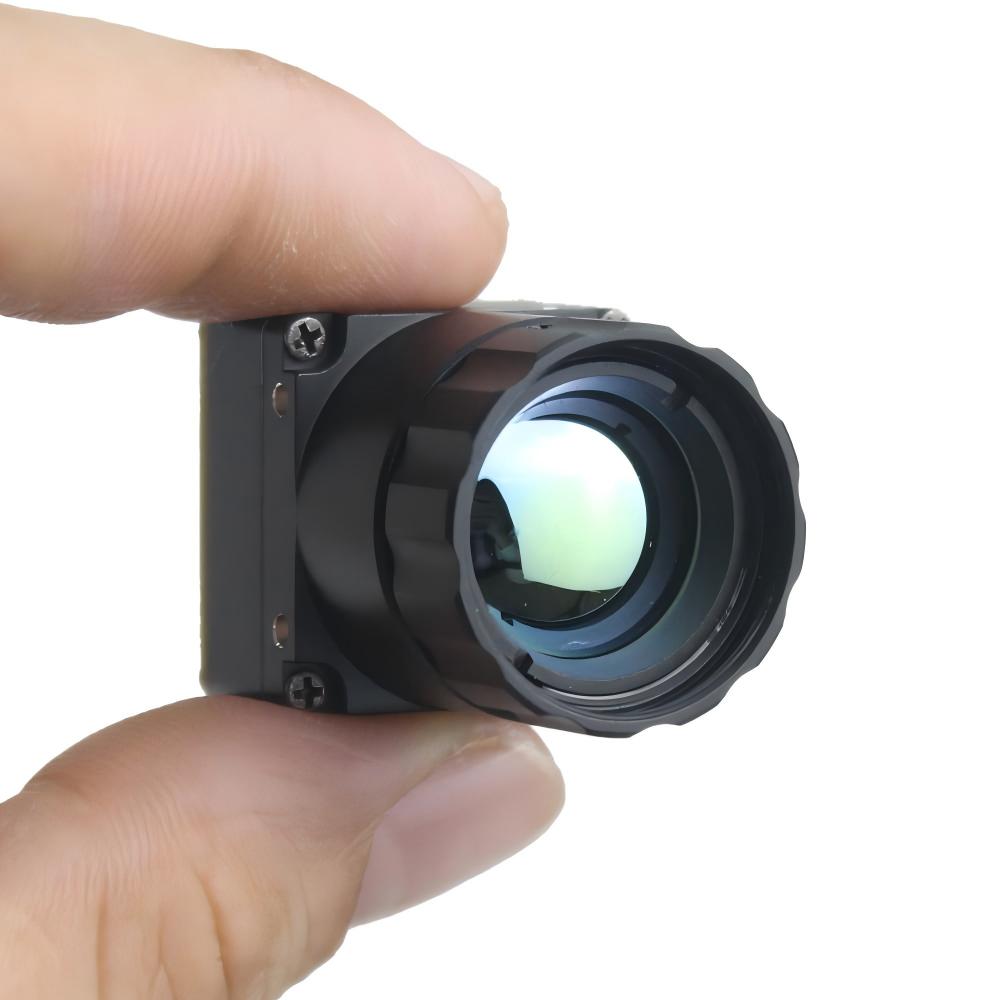
| Physical Dimensions | Ultra-compact micro module package | Mini-Size of 21 mm × 21 mm |
| Available Focal Lengths | Fixed wide-angle standard industrial lens | 5 / 9 / 13 / 18 / 35 / 50 / 75 / 100 / 150 mm |
| Hardware Interface Formats | Raw streaming radiometry / Digital Video | Direct USB Class Compliant / Digital Core |
| Target Application Space | Mine detection, localized PCB diagnosis | Long-range aerial drones, surveillance, Edge AI |
Comprehensive Product Analysis
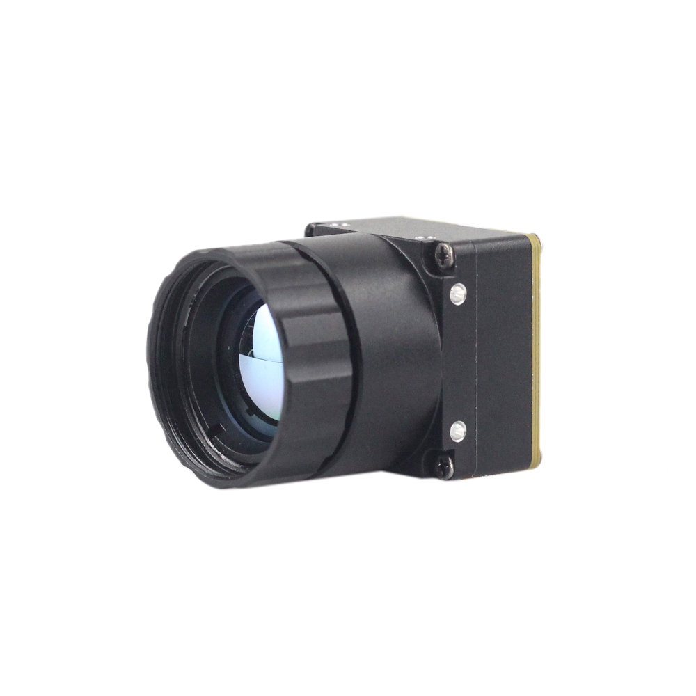
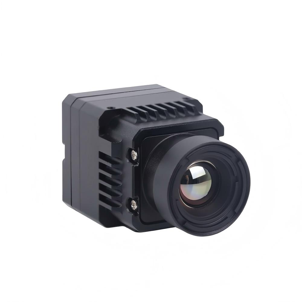
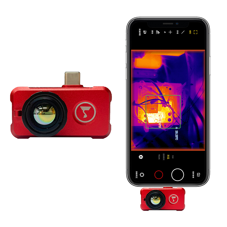
Uncooled LWIR Mini 256*192 Thermal Imaging Camera Module Similar To DJI For Detecting Mines
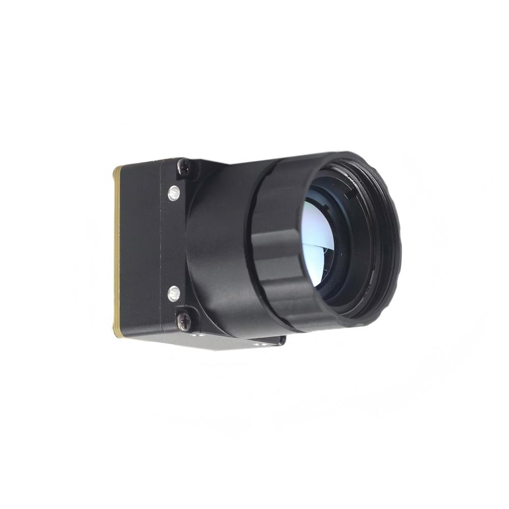
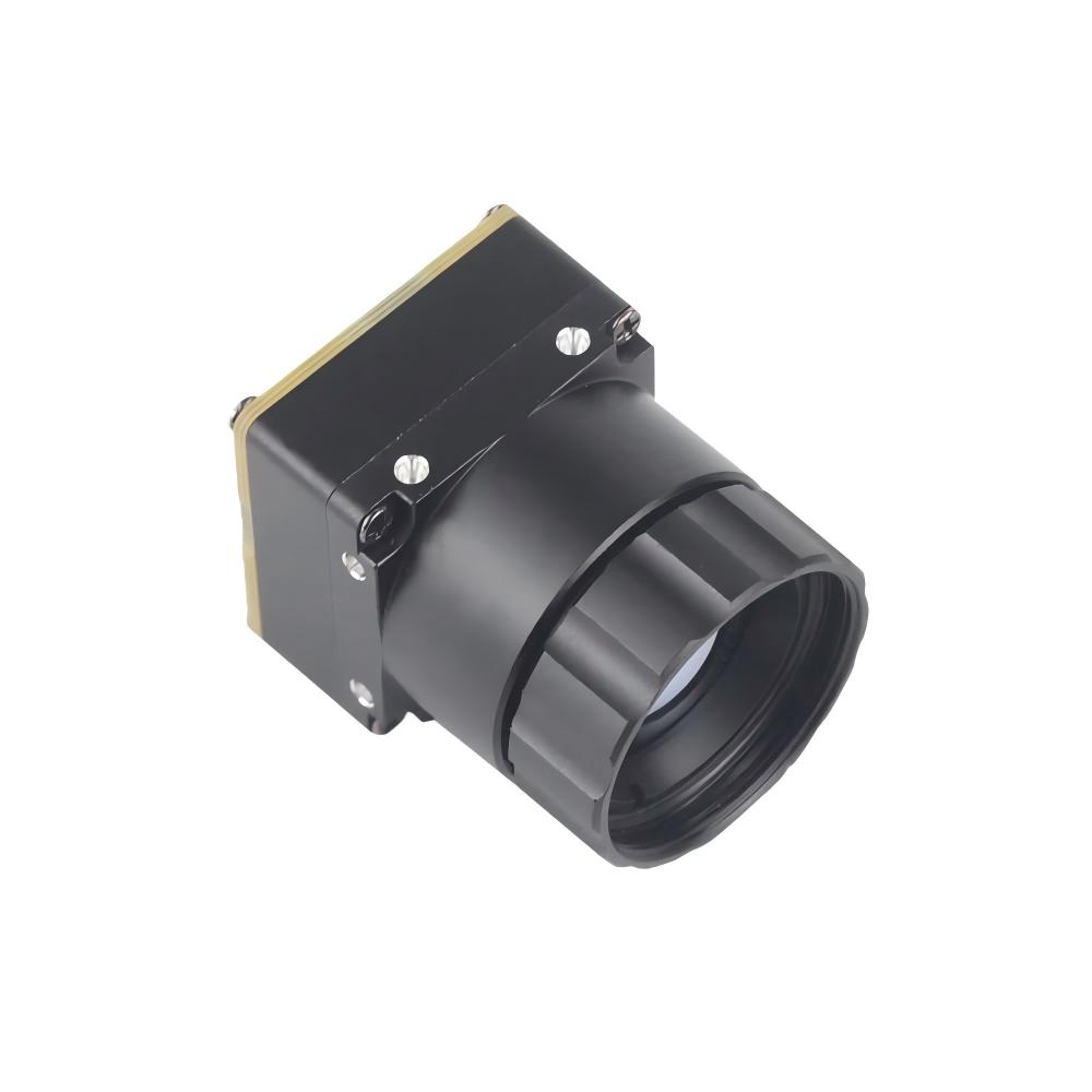
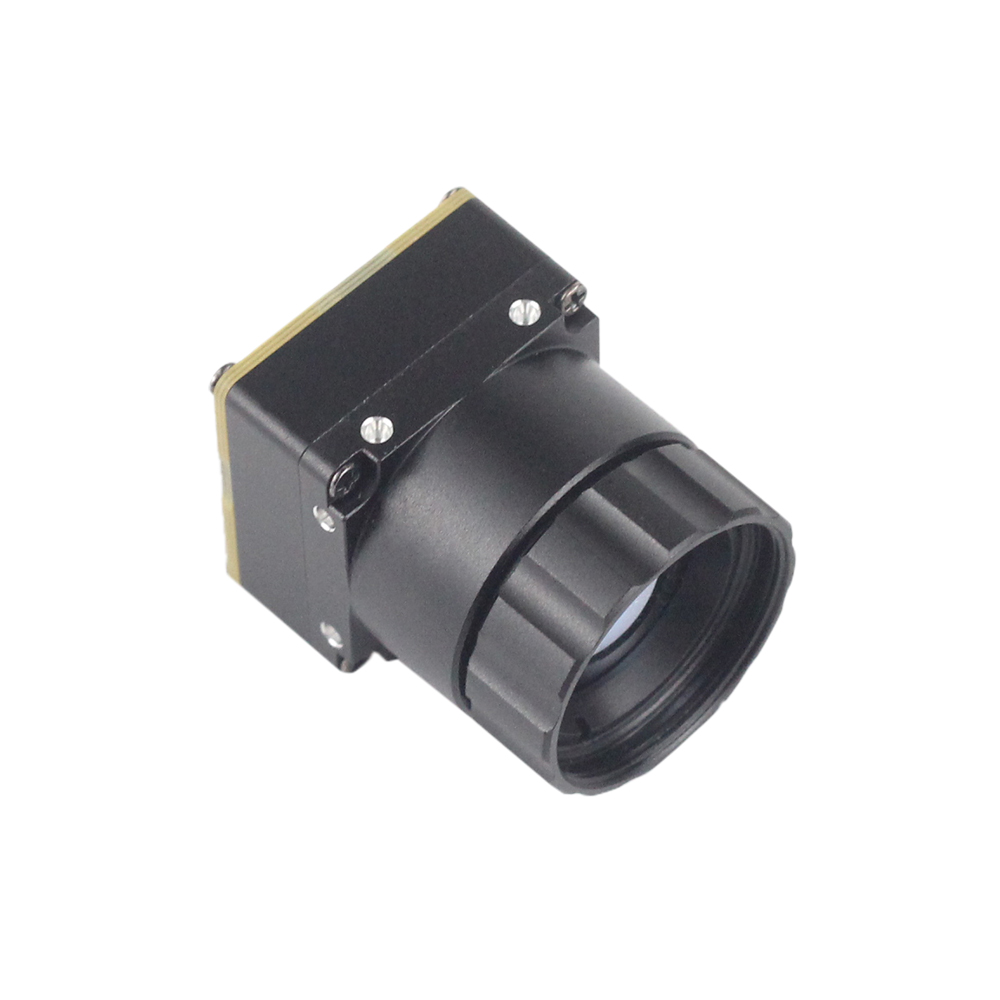
The Mini 256 Uncooled LWIR thermal Camera Module adopts high-performance infrared detectors for ultra-clear thermal imaging and accurate temperature measurement. It captures infrared radiation and outputs a uniform thermal image with radiometry. Engineered specifically for weight-sensitive applications such as autonomous micro-drones, robotic detection arms, and explosive ordnance reconnaissance equipment, this module delivers calibrated radiometric data in a compact form factor.
The core uses a 256 × 192 VOx microbolometer array operating within the 8 μm to 14 μm spectral band, maintaining thermal sensitivity down to ≤ 50 mK. Its onboard signal processing engine automatically corrects for sensor drift across operating temperatures, outputting stable radiometric frames suitable for integration into automated landmine detection and localized thermal inspection systems.
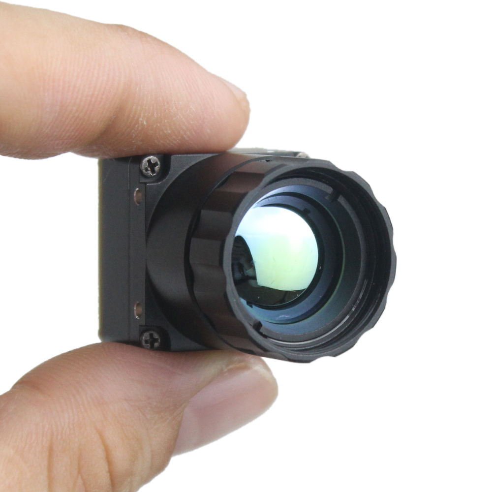
Uncooled LWIR USB Mini 640*512 Thermal Imaging Camera Core Module For Drones Similar To DJI
The Mini uncooled infrared thermal imaging module features sharp, crisp image presentation, compact dimensions, and low system integration costs. Designed with a tiny housing profile of just 21 mm × 21 mm, this 640 × 512 / 640 × 480 core module provides high environmental adaptability, stable performance across wide temperature ranges, and broad lens compatibility.
The module supports a wide variety of lens configurations, including 5 mm, 9 mm, 13 mm, 18 mm, 35 mm, 50 mm, 75 mm, 100 mm, and 150 mm focal lengths. This versatility allows engineers to configure the camera for everything from wide-angle aerial mapping to long-range telephoto surveillance. The direct USB interface simplifies hardware integration with embedded single-board computers, delivering plug-and-play radiometric video without requiring custom external interface boards. To explore detailed bench evaluations of this core, read our deep-dive analysis on Mini 640 performance benchmarks.
7. Mission-Critical Deployment: PCB Diagnostics, Aerial Surveillance & Edge AI
Micro-Scale PCB Electronics Diagnostics
In modern multi-layer PCB design and manufacturing, locating component-level faults is a primary diagnostic challenge. High-density surface-mount packaging, internal power planes, and compact component arrangements make traditional probing difficult and slow. A common failure mode is dielectric breakdown in multi-layer ceramic capacitors (MLCCs). When these capacitors degrade, they rarely fail with obvious physical damage; instead, they develop high-resistance internal leakage paths.
These sub-surface micro-shorts draw continuous parasitic currents from supply rails, resulting in localized temperature increases of just 0.5°C to 3.0°C. High-sensitivity uncooled LWIR cameras equipped with macro lenses can resolve these minor thermal gradients. An engineer can power the board with a current-limited bench supply and instantly identify the damaged capacitor on the thermal display. The thermal camera highlights the failing component while surrounding parts remain at ambient temperature, avoiding hours of trial-and-error component desoldering.
Aerial Landmine and UXO Detection
Surface-laid and shallowly buried unexploded ordnance (UXO), landmines, and improvised explosive devices (IEDs) present complex detection challenges in humanitarian demining operations. These targets can be identified aerially by exploiting diurnal solar heating cycles and the differing thermal properties of soil and ordnance materials.
Soil directly above a buried object has a lower effective thermal mass than surrounding undisturbed earth. Consequently, undisturbed soil and buried casings absorb and release solar heat at different rates:
- ⚙️ Morning Solar Heating Cycle: As solar radiation heats the ground, the shallow layer of soil covering a buried mine warms faster than deeper, consolidated earth. On a thermal camera mounted to an aerial drone, these locations appear as distinct hot spots.
- ⚙️ Thermal Inversion Point: As afternoon transition periods approach, the temperatures of the soil and the target temporarily equalize. This brief crossover point temporarily masks the thermal signature of the buried object.
- ⚙️ Evening Radiative Cooling Cycle: After sunset, the thin layer of soil above the ordnance radiates heat rapidly into the cooler night sky, losing thermal energy faster than the surrounding bulk earth. The anomaly inverts, showing up on the thermal imager as a localized cool spot.
Deploying compact cores like the Mini 256 or Mini 640 on autonomous reconnaissance drones allows operators to map hazardous minefields from a safe standoff distance, reducing risks during route clearance operations.
Automated Manufacturing Vision & Edge AI
Modern manufacturing facilities increasingly deploy thermal cameras alongside visible machine vision systems on automated production lines. Applications include inspecting three-phase industrial electrical panels, monitoring bearing friction in conveyor drive systems, and verifying laser welding seam integrity in automotive manufacturing.
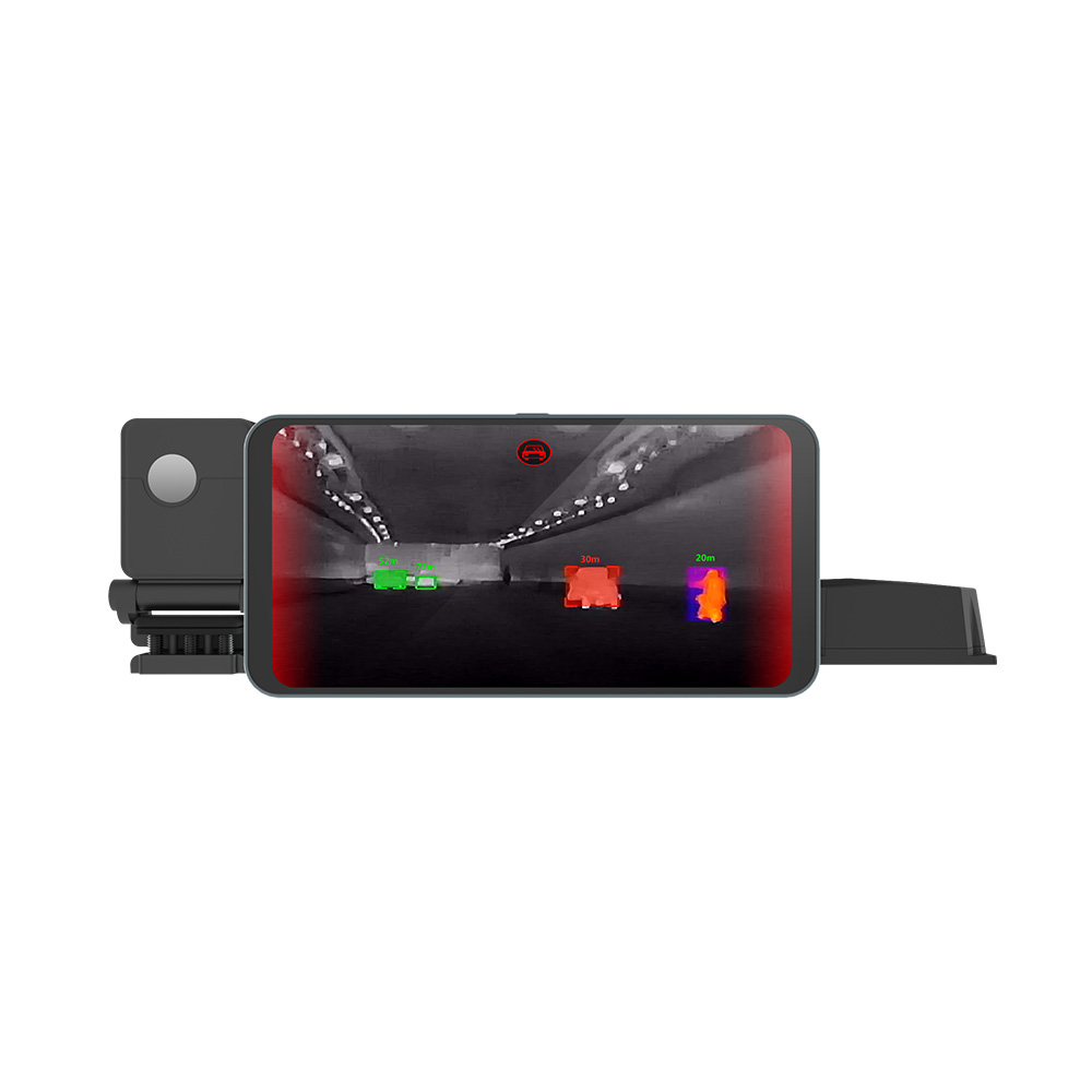
In these environments, thermal cores stream uncompressed 16-bit radiometric video directly to on-device edge AI processors over USB or MIPI connections. Deep convolutional neural networks (such as YOLOv8) run directly on the temperature data array, rather than on standard 8-bit colorized video. Because each pixel corresponds to a calibrated temperature reading, edge AI models can detect thermal threshold violations, trace heat dissipation patterns, and trigger automated alerts before equipment failures cause line shutdowns.
8. Deep-Dive Engineering FAQ
Are budget thermal imaging cameras under $400 suitable for professional electronics and HVAC diagnostics?
What is the operational difference between 256x192 and 640x512 thermal imaging resolutions?
Can compact thermal camera modules be embedded directly into custom drones and edge AI hardware?
📚 References & Further Reading
- Industry Standard: High-density micro-coaxial connectors and embedded interconnect solutions via Molex
- Industry Standard: Single-board edge computing architectures and driver platforms via Raspberry Pi
- Related Guide: Mini 640 Thermal Camera Core Performance Evaluation
- Related Guide: RS300 Thermal Camera Driver Configuration for Raspberry Pi
- Related Guide: High-Resolution LWIR Streaming Camera Modules for Raspberry Pi