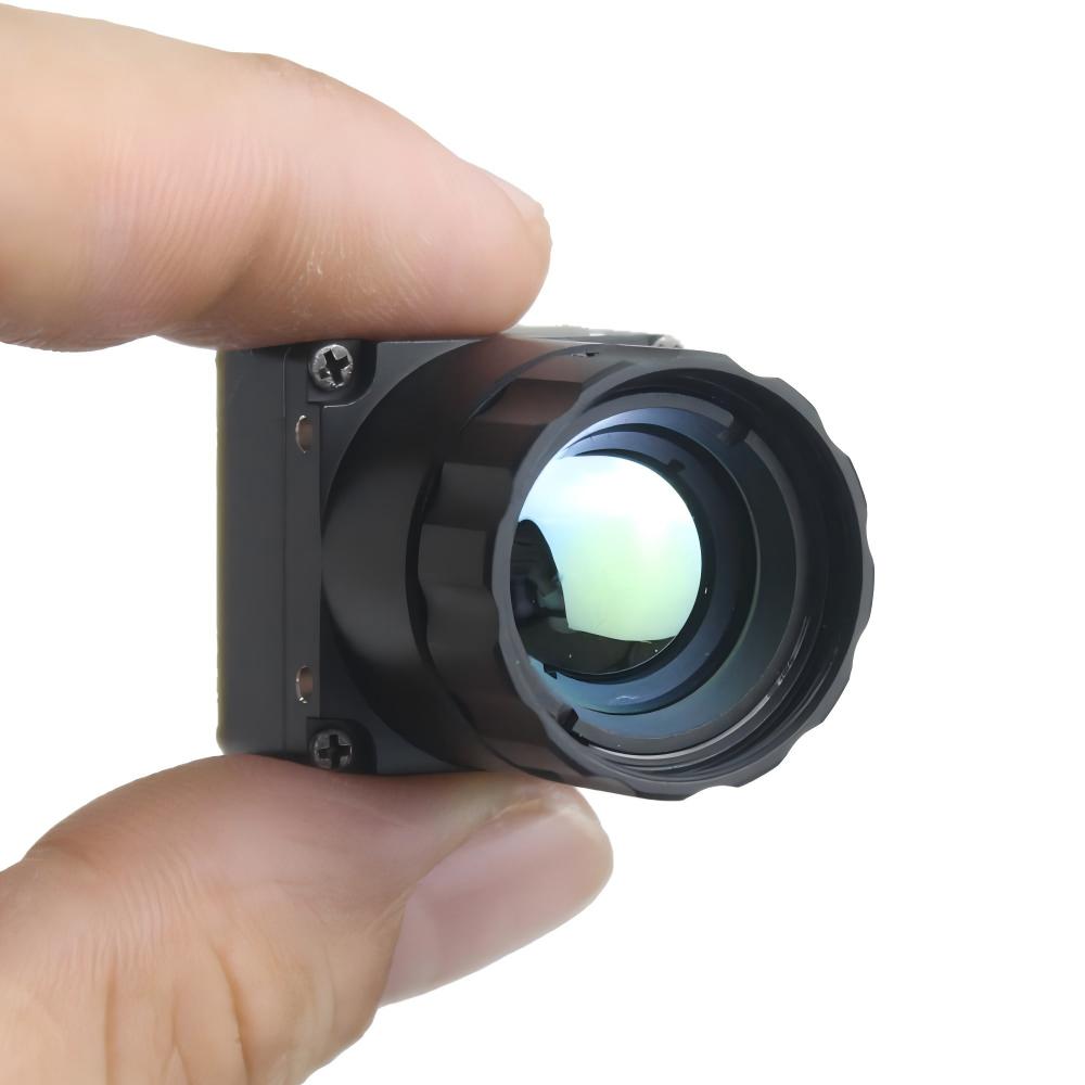
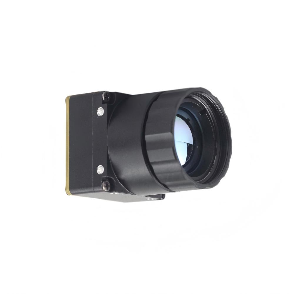
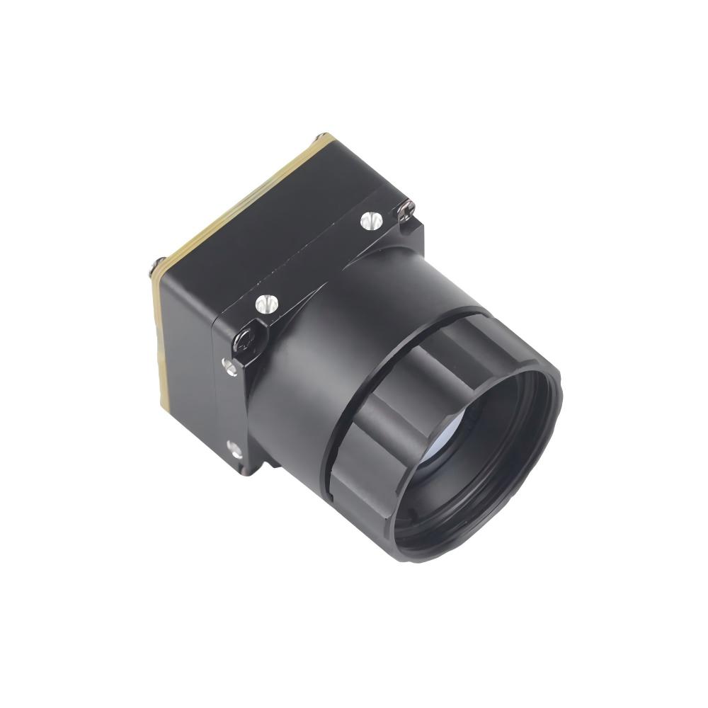
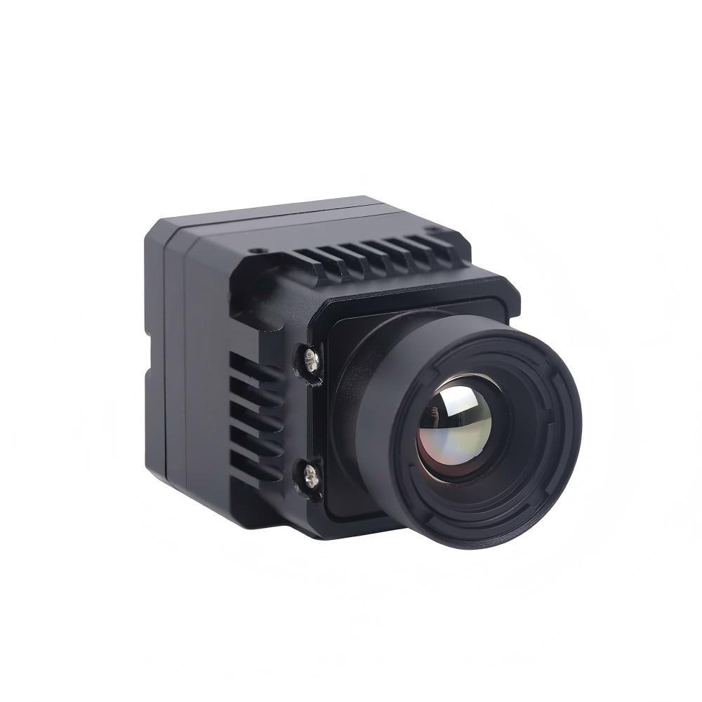
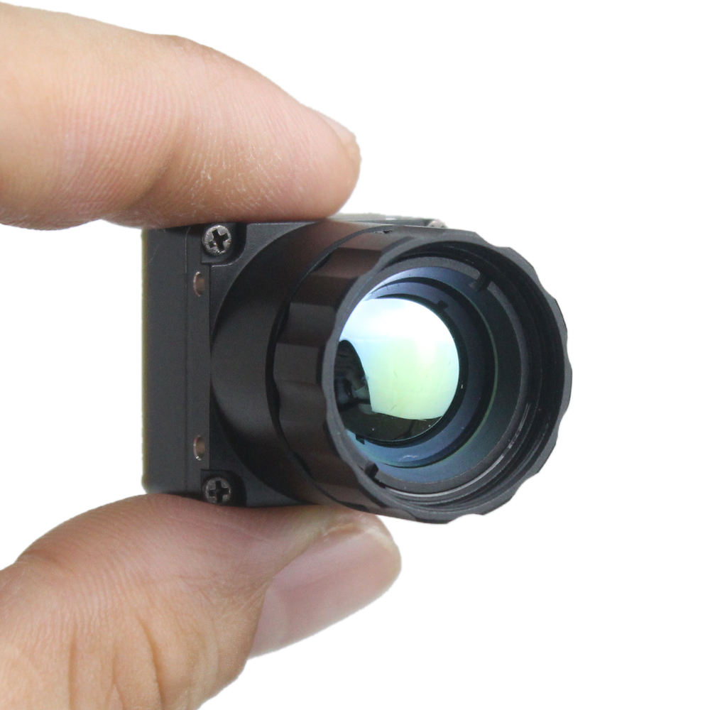
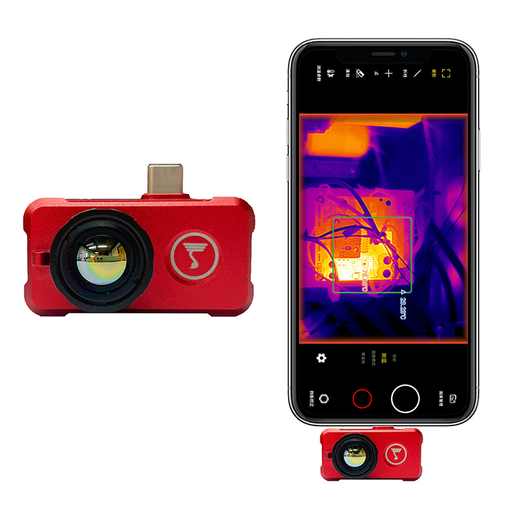
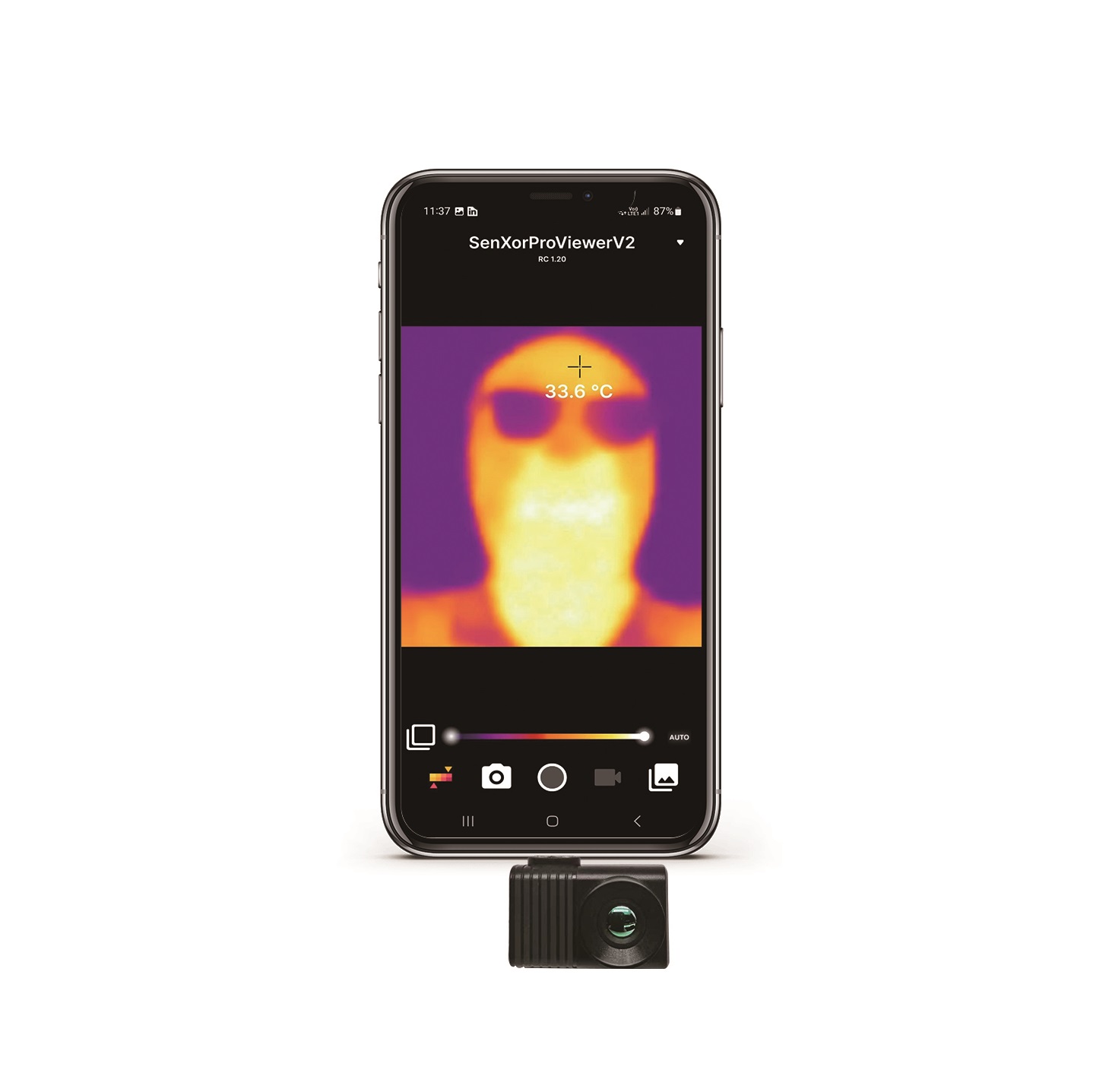
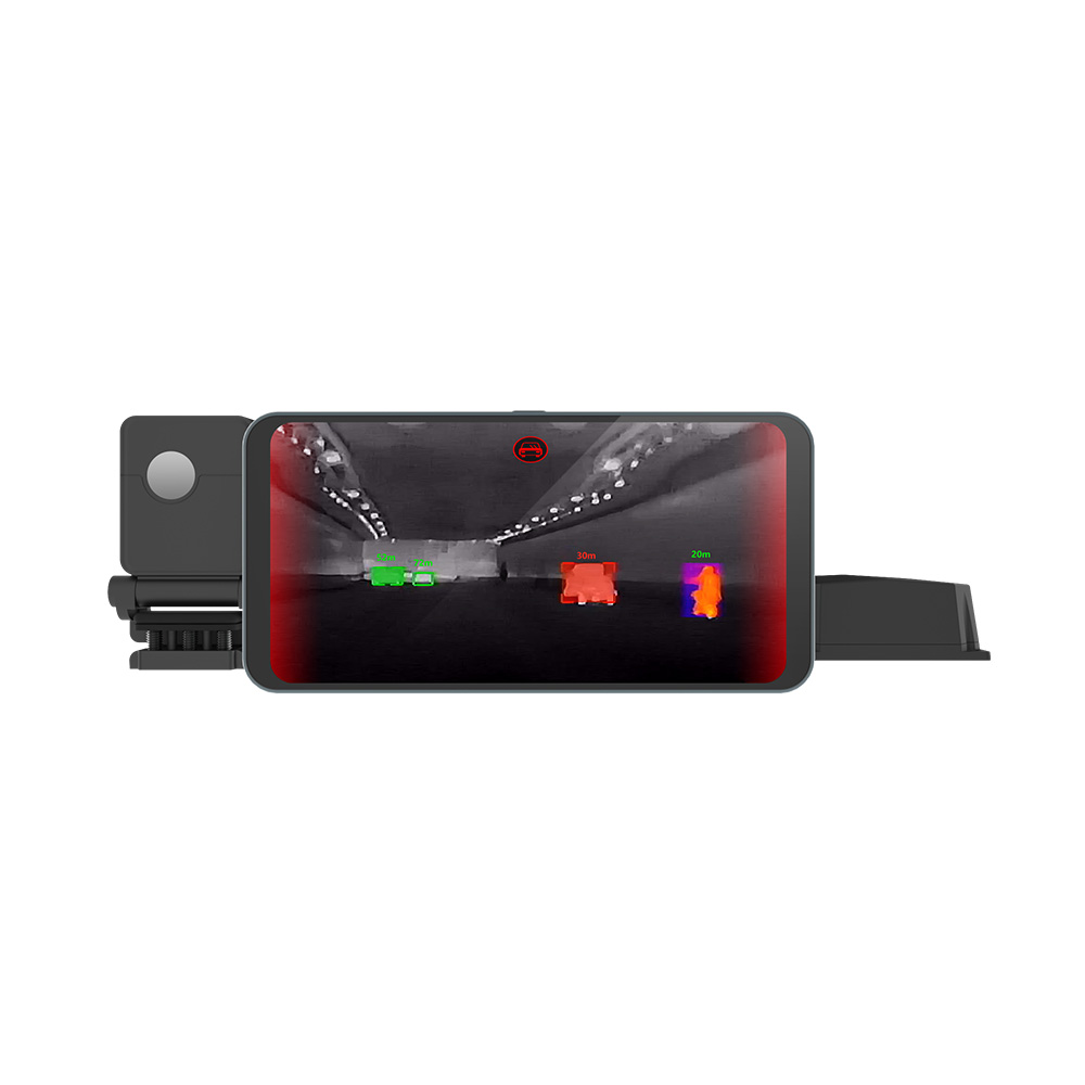

384x288 Thermal Camera Module: The Sweet-Spot Sensor for Drones & Machine Vision
2026年8月25日
High Resolution Thermal Imaging: 1280x1024 LWIR Sensor Modules & OEM Solutions
2026年8月26日
1280x1024 Thermal Module: Next-Gen HD Infrared Core Integration Guide
If you have spent any time at the test bench designing electro-optical and infrared (EO/IR) payloads, you know the harsh reality of long-wave infrared (LWIR) physics: standard-definition VGA (640x512) has hit its hard operational limits. Jumping to a high-definition SXGA 1280x1024 thermal module is easily the most significant architectural leap uncooled thermal imaging has seen in twenty years. Systems engineers in aerospace, defense, factory automation, and drone manufacturing all run into the exact same wall. You need to double or triple your operational target detection ranges, but you cannot afford to quadruple optical payload weight, burn through limited battery reserves, or choke your embedded data buses. Packing over 1.31 million active microbolometer pixels onto a single focal plane array (FPA) with a tight 12μm pixel pitch gives you four times the spatial resolution of legacy VGA sensors. That structural change completely rewires standard Johnson's Detection, Recognition, and Identification (DRI) envelopes, letting airborne gimbals and field optics lock onto subtle, low-contrast thermal signatures at long standoff ranges while keeping the front optical elements remarkably compact.
Here is the deal: dropping an ultra-high-resolution uncooled infrared imaging core into modern size, weight, power, and cost (SWaP-C) constrained platforms—whether that is a three-axis drone gimbal, an autonomous mobile robot (AMR), a handheld weapon sight, or a machine-vision inspection rig—is not a simple plug-and-play job. You are dealing with uncompressed 16-bit raw digital video pushing past 1.25 Gbps at 50Hz or 60Hz, parasitic thermal loads trapped inside sealed enclosures, focal drift across harsh temperature swings, and the need for deterministic, ultra-low-latency signal processing for edge AI computer vision. This technical integration guide breaks down the microbolometer physics, modulation transfer function (MTF) dynamics, digital interface pipelines, edge AI workflows, and factory radiometric calibration routines you need to master to successfully deploy a modern 1280x1024 thermal module in the field.
Table of Contents
- 👉 1. The Architectural Leap: Why 1280x1024 HD Infrared Cores Redefine Thermal Sensing
- 👉 2. Optical Design, MTF, and Pixel Pitch Dynamics
- 👉 3. High-Throughput Digital Interfaces and Edge AI Video Pipelines
- 👉 4. SWaP-C Optimization: Mechanical, Thermal, and Harnessing Integration
- 👉 5. Purpleriver High-Performance Thermal Module Lineup & Specifications
- 👉 6. Mission-Critical Deployment Scenarios & System Architectures
- 👉 7. OEM Calibration, NUC, and Radiometric Workflow Best Practices
- 👉 8. In-Depth Engineering FAQ
- 👉 9. Conclusion & Engineering Resources
1. The Architectural Leap: Why 1280x1024 HD Infrared Cores Redefine Thermal Sensing
The operational effectiveness of any thermal imaging platform comes down to one metric: how many real spatial detector elements you can put across your target. On a standard 640x512 microbolometer, a vehicle or human target at three to four kilometers covers barely a 2x2 or 3x3 pixel patch on the focal plane. Under Johnson’s criteria, that level of spatial sampling gives you just enough energy contrast for basic detection—you know something hot is out there, but you cannot tell if it is an armored personnel carrier, a civilian pickup, or background clutter. A 1280x1024 thermal module changes the equation entirely by providing a native array of 1,310,720 active VOx detector pixels. By delivering four times the pixel density across the exact same field of view, that identical target now lights up an 8x8 or 12x12 pixel grid. That spatial jump moves your data pipeline immediately from vague detection into positive recognition and reliable kinematic tracking.
Getting this pixel density into an uncooled, sub-miniature form factor requires top-tier MEMS fabrication and precision thin-film material science. Modern HD microbolometers rely on Vanadium Oxide (VOx) thin films rather than legacy Amorphous Silicon (a-Si). VOx provides a much higher Temperature Coefficient of Resistance (TCR), typically sitting between -2.0%/K and -3.2%/K, along with significantly lower 1/f flicker noise. When you shrink detector pixel pitch to 12μm, the physical surface area available to capture incoming long-wave infrared radiation (the 8μm to 14μm atmospheric window) drops to just 144 square micrometers per pixel. To maintain high thermal sensitivity—specifically an NETD (Noise Equivalent Temperature Difference) under 35mK to 40mK at f/1.0—foundries implement three crucial hardware innovations:
- ⚙️ Sub-Micron Vacuum Suspension Bridges: Each individual microbolometer pixel is suspended over the readout silicon by micro-machined silicon nitride legs. These ultra-narrow legs maximize thermal isolation (slashing thermal conductance, Gth) so tiny shifts in absorbed infrared energy produce measurable temperature swings, all while holding the thermal time constant under 10 to 12 milliseconds to eliminate motion smear during fast pans.
- ⚙️ Resonant Cavity Optical Absorbers: Underneath the bridge, a quarter-wavelength integrated reflector creates a tuned Fabry-Pérot resonant cavity. This structure forces destructive interference absorption across the 8–14μm band, driving total absorption efficiency above 90% despite the reduced physical volume of the 12μm detector.
- ⚙️ Ultra-Low-Noise Column-Parallel ROICs: Reading out 1.31 million analog signals at 60Hz without cooking the sensor with parasitic self-heating demands sub-micron CMOS Readout Integrated Circuit (ROIC) architectures. High-speed column-parallel ADCs digitize the microbolometer signal right at the array perimeter, wiping out analog line loss, cutting crosstalk, and streaming pristine 14-bit or 16-bit linear radiometric counts directly to the system ISP.
For systems engineers reviewing broader electro-optical configurations across border defense and industrial payloads, our detailed engineering breakdown on thermal camera core integration in regional security covers foundational operational parameters, radiometric principles, and baseline deployment criteria across complex operational theatres.
2. Optical Design, MTF, and Pixel Pitch Dynamics
Look at the optical physics: upgrading an optomechanical design from a 640x512 array to an HD 1280x1024 sensor completely transforms your lens design requirements. The physical diagonal of a 12μm 1280x1024 sensor measures roughly 19.67mm (15.36mm horizontal by 12.288mm vertical). In contrast, a 12μm 640x512 sensor has an active diagonal of only 9.83mm. You cannot just slap standard small-format LWIR glass in front of an HD core. If you try, you will immediately run into severe optical vignetting, extreme light falloff at the borders, field curvature, and serious chromatic aberrations across the outer 50% of your image plane.
The spatial Nyquist frequency of an infrared detector is fixed strictly by its physical pixel pitch. For a 12μm microbolometer array, the spatial Nyquist limit works out to:
Nyquist Frequency (f_Nyquist) = 1 / (2 × Pixel Pitch) = 1 / (2 × 0.012 mm) = 41.67 line pairs per millimeter (lp/mm)
To take full advantage of a 1.3-megapixel thermal array without suffering from severe MTF degradation and image softening, your optical objective must deliver high Modulation Transfer Function performance all the way out to that 41.67 lp/mm cutoff across the entire 19.67mm image circle. In the shop, hitting this level of optical resolution requires careful optical material selection and active thermal compensation:
- ⚙️ Monocrystalline Germanium (Ge): Germanium remains the workhorse material for high-resolution LWIR optics due to its high refractive index (around 4.0 at 10μm), enabling fast, compact elements with minimal spherical aberrations. But Germanium has a massive thermal refractive index drift (dn/dT ≈ 3.96 × 10⁻⁴ / °C). Without compensation, a simple 15°C ambient shift will throw a 12μm HD core completely out of focus. You must integrate mechanical athermalization linkages (combining materials with opposing thermal expansion coefficients like Delrin, Invar, and aluminum) or active motorized focus routines across the -40°C to +80°C envelope.
- ⚙️ Chalcogenide Glass Formulations (e.g., GASIR, BD6): Advanced chalcogenide materials feature a substantially lower dn/dT than Germanium. By pairing single-point diamond-turned (SPDT) aspheric and diffractive elements in a hybrid Germanium-Chalcogenide doublet or triplet group, you can design highly stable, passively athermalized fixed-focus optics built specifically for airborne drone gimbals.
- ⚙️ Photonic Speed vs. Lens Weight (f/1.0 vs. f/1.2): While an f/1.0 aperture pulls in maximum thermal flux to achieve that clean sub-35mK NETD, the large clear aperture drastically increases front-element glass mass. In payload-restricted drone designs, engineering your lens around an f/1.2 or f/1.25 aperture cuts front-element weight by 35% to 45%. Modern ASIC-level spatial-temporal noise filters and deep-learning denoisers readily make up for the slight reduction in raw photonic flux.
For an expanded comparison of optical focal lengths and multi-aperture configurations across tactical platforms, check out our comprehensive industry guide on the best thermal camera cores for drone and robotic integration.
3. High-Throughput Digital Interfaces and Edge AI Video Pipelines
The biggest roadblock engineers hit when integrating a 1280x1024 thermal imaging core into an embedded architecture is the raw digital data bandwidth. Because uncooled microbolometers output linear digital signal values directly tied to scene radiance, precise thermography and tactical image enhancement algorithms require uncompressed 14-bit or 16-bit raw radiometric frames. Running a full 60Hz frame rate, the uncompressed data rate from a 1280x1024 core clocks in at:
Raw Bandwidth = 1280 × 1024 pixels × 16 bits/pixel × 60 frames/sec = 1,258,291,200 bits/sec ≈ 1.258 Gbps
Old-school SPI buses, legacy parallel CMOS rails, and standard USB 2.0 links simply fall flat under this volume of data. Forcing a continuous 1.26 Gbps uncompressed stream through legacy interconnects leads straight to dropped frames, severe packet jitter, and unpredictable latency—unacceptable flaws when you are running high-speed robotic navigation, aerial target tracking, or automated counter-UAS systems.
To eliminate these bottlenecks, modern 1280x1024 thermal modules implement specialized high-speed physical interfaces tailored to embedded processing architectures:
- ✅ MIPI CSI-2 (Camera Serial Interface): The industry standard for robotic vision and tight drone payloads. Running across a high-speed 2-lane or 4-lane D-PHY physical layer, MIPI CSI-2 pipes uncompressed 14-bit/16-bit raw digital video straight into the hardware image signal processors (ISP) and DMA buffers of edge microprocessors like the NVIDIA Jetson Orin, Xavier, and industrial ARM application processors. This direct memory access bypasses the host CPU, locking in sub-20ms glass-to-glass latency and zero-copy memory access for deep-learning object detection models.
- ✅ Sub-LVDS and Parallel CMOS: The preferred choice for custom FPGA architectures (such as AMD Xilinx Zynq UltraScale+ or Intel Cyclone platforms). Sub-LVDS provides deterministic, low-EMI differential signaling across internal board-to-board interconnects, making it ideal for rugged vehicle turrets, weapon sights, and high-shock naval mounts.
- ✅ Industrial IP Networking (GigE Vision / RJ45 RTSP): For perimeter defense, industrial process automation, and critical infrastructure monitoring, an onboard hardware compression engine allows direct RTSP/ONVIF streaming over standard Ethernet. The onboard processor encodes raw thermal frames into H.264/H.265 while simultaneously passing radiometric temperature telemetry over dedicated TCP/IP ports.
To crunch dynamic image enhancement across 1.31 million pixels every 16.6 milliseconds, the core's onboard ASIC executes dedicated hardware-accelerated processing pipelines:
- ⚙️ Hardware-Accelerated Two-Point NUC: Wipes out spatial fixed-pattern noise across all 1.31 million pixels in real time using dedicated on-chip math units.
- ⚙️ Dynamic Digital Detail Enhancement (DDE+): Applies multi-scale spatial decomposition filters that pull high-frequency target edges out of low-contrast thermal backgrounds without generating halo artifacts or unnatural edge ringing around hot targets.
- ⚙️ Multi-Scale Adaptive Gain Control (AGC): Compresses the raw 14-bit dynamic range into clean 8-bit display video, ensuring human and vehicle profiles remain sharp and clear even when high-temperature flares or fires enter the frame.
4. SWaP-C Optimization: Mechanical, Thermal, and Harnessing Integration
Integrating a high-resolution 1280x1024 thermal module into tight SWaP-C designs demands serious attention to mechanical, thermal, and electrical pathing. Uncooled microbolometers do away with the bulky, power-hungry cryogenic Stirling coolers used in MWIR systems, but the uncooled focal plane remains extremely sensitive to conducted and radiated thermal gradients inside the camera housing.
If parasitic heat from a host processor, voltage regulators, or brushless gimbal motors soaks unevenly into the sensor chassis, a dynamic thermal gradient forms across the microbolometer array. That uneven thermal profile causes localized pixel drift, showing up on screen as nasty vertical banding, vignetting artifacts, and false radiometric readings. You need to use high-conductivity thermal interface gap pads (exceeding 5.0 W/m·K) to conduct heat away from the internal ASIC and power stages directly out to the external aluminum structural housing. Modern 1280x1024 cores also mount precision thermistors right on the FPA substrate and inside the lens barrel. The ASIC tracks these thermistors in real time, referencing multi-dimensional calibration lookup tables (LUTs) to adjust detector bias voltages and offset matrices without forcing a mechanical shutter drop during mission operations.
In three-axis continuous-rotation gimbals and pan-tilt turrets, routing wideband MIPI CSI-2 or USB 3.0 lines through miniature slip rings introduces serious high-frequency attenuation, impedance mismatches, and EMI noise. Seasoned systems integrators turn to micro-coaxial cable assemblies manufactured by specialized harness leaders such as Micro Coaxial Cable Man. These miniature cable bundles use ultra-fine 42 to 46 AWG shielded lines that hold tight 50-ohm single-ended and 100-ohm differential impedance across multi-gigahertz frequencies. Their ultra-thin, high-flex build minimizes mechanical torque resistance inside compact gimbal pitch and yaw joints, preventing motor oscillations and significantly extending payload operating life.
5. Purpleriver High-Performance Thermal Module Lineup & Specifications
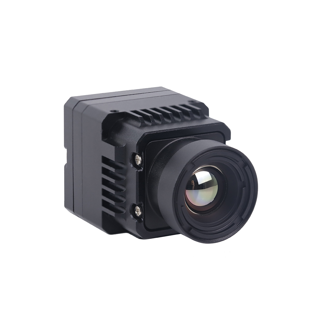
To support diverse embedded applications—from micro-unmanned aerial vehicles and tactical thermal weapon sights to continuous-duty industrial monitoring platforms—Purpleriver designs and manufactures an industry-leading portfolio of uncooled LWIR camera modules. The technical matrix below compares our mainstream 640x512 micro-cores against our flagship high-definition 1280x1024 architecture.
| System Parameter | Mini2 640x512 MIPI Module | ASIC 640x512 RJ45/IP Module | Flagship 1280x1024 HD Module |
|---|---|---|---|
| Hardware Imagery |
|
|
HD 1280x1024 VOx Core
|
| Sensor Resolution | 640 × 512 pixels | 640 × 512 pixels | 1280 × 1024 pixels (SXGA) |
| Pixel Pitch | 12 μm | 12 μm | 12 μm |
| Detector Architecture | Uncooled VOx Microbolometer | Uncooled VOx Microbolometer | Uncooled VOx Microbolometer |
| Spectral Response | 8 to 14 μm (LWIR) | 8 to 14 μm (LWIR) | 8 to 14 μm (LWIR) |
| Thermal Sensitivity (NETD) | ≤ 40 mK @ f/1.0, 300K | ≤ 40 mK @ f/1.0, 300K | ≤ 35 mK @ f/1.0, 300K |
| Digital Output Protocols | MIPI CSI-2, DVP Parallel, USB | RJ45 Ethernet (RTSP/ONVIF), CVBS | MIPI CSI-2 (4-Lane), USB 3.0, LVDS |
| Max Output Frame Rate | 25Hz / 30Hz / 50Hz | 25Hz / 30Hz / 50Hz | 50Hz / 60Hz Full Frame |
| Typical Power Draw | < 0.8 W (Ultra-Low SWaP) | < 1.5 W (Full IP Stack) | < 1.6 W (Full HD Processing) |
| Operating Temperature | -40°C to +80°C | -40°C to +80°C | -40°C to +85°C Industrial/Mil |
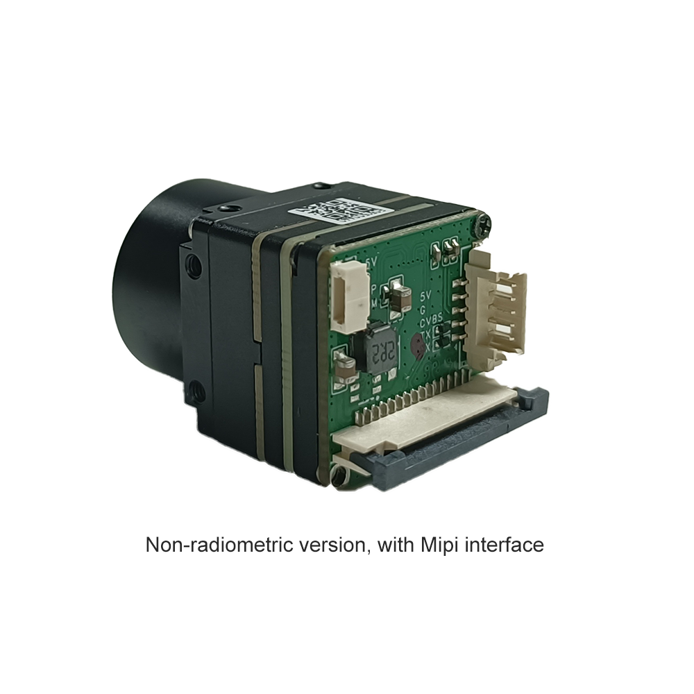
Mini2 640x512 MIPI Thermal Imaging Camera Module
The Uncooled Infrared Mini2 640x512 9mm Thermal Imaging Camera Module For Drones is engineered specifically for ultra-compact commercial and defense micro-drones where every milligram of payload mass impacts flight endurance. Featuring a compact form factor, low power draw under 0.8W, and direct MIPI CSI-2 digital video integration, this module delivers exceptionally sharp, high-contrast thermal imagery across dynamic flight envelopes.
View Product Details & Pricing ➔
ASIC 640x512 RJ45/CVBS RTSP IP Thermal Sensor Module
The Uncooled Infrared Mini 640x512 ASIC Thermal Imaging Camera Module For Drones integrates an onboard hardware network encoder and complete RTSP/ONVIF streaming stack. Engineered for industrial PTZ security cameras, autonomous mobile robotics, and long-range perimeter monitoring, it delivers simultaneous digital IP video streaming and legacy analog CVBS composite output for maximum installation versatility.
View Product Details & Pricing ➔
6. Mission-Critical Deployment Scenarios & System Architectures
The spatial resolution and low-latency pipeline of a 1280x1024 thermal module unlock decisive operational upgrades across several high-consequence industries:
Airborne Tactical ISR
On small Group 1 and Group 2 unmanned aerial systems, payload capacity is strictly limited—often capped under 450 grams. Achieving standoff target identification previously required heavy continuous-zoom lenses paired with 640-class sensors. Integrating a 1280x1024 module with a compact 50mm f/1.2 athermal lens allows an airborne platform cruising at 2,000 feet AGL to hold a broad 17.5-degree horizontal FOV while retaining enough spatial pixels to detect vehicles past 5.0 kilometers and classify humans at 1.8 kilometers. You maintain complete situational awareness across the scene while the 1.3-megapixel density allows deep digital cropping without turning the image into digital noise.
Autonomous AI Target Tracking and Slew-to-Cue
Edge AI platforms deployed on perimeter security ground vehicles and counter-UAS platforms depend on clean structural edge data to run convolutional inference models without throwing false alarms. Ingesting raw 16-bit thermal video over MIPI CSI-2 directly into an NVIDIA Jetson Orin running TensorRT-accelerated YOLO models provides four times the pixel data per target. This pixel density stabilizes bounding boxes, keeps target locks locked through dust, fog, and obscurants, and delivers high-precision coordinate data to cue co-aligned laser rangefinders or kinetic systems.
High-Voltage Radiometry and Predictive Maintenance
In power utility drone inspections and industrial plant monitoring, non-contact thermal measurement accuracy is governed by the Spot Size Ratio (SSR). SSR dictates the minimum target dimension required to fill a detector pixel without background temperature bleed. With a 1280x1024 12μm array, your SSR doubles compared to a 640x512 array using identical focal length optics. Utility inspection teams can accurately measure hot spots on transformer bushings, isolators, and splices from twice the standoff distance, keeping flight hardware well clear of high-voltage induction hazards.
7. OEM Calibration, NUC, and Radiometric Workflow Best Practices
Getting dependable field performance out of an uncooled 1280x1024 sensor requires disciplined calibration routines and rigorous signal correction practices:
Non-Uniformity Correction (NUC) Protocols
Every single pixel in a 1.3-megapixel array has slight manufacturing variations in its responsivity (gain) and baseline voltage (offset). Left uncorrected, fixed-pattern noise (FPN) will quickly blind the sensor in low-contrast scenes:
- ⚙️ Mechanical Solenoid Shutter Correction: Standard cores use an internal electromagnetic shutter to present an isothermal blackbody reference across the array. Essential during initial boot and sudden ambient temperature spikes, dropping the shutter too frequently interrupts video feeds and breaks AI tracking locks. Advanced ASIC firmware limits shutter drops to once every 20 to 30 minutes by continuously checking internal substrate thermistors and running real-time polynomial drift compensation.
- ⚙️ Scene-Based Non-Uniformity Correction (SBNUC): For guided munitions, counter-UAS tracking turrets, or fast aerial maneuvers where a 300ms video freeze is unacceptable, SBNUC algorithms calculate high-order spatial noise filters on the fly by analyzing frame-to-frame scene motion, eliminating the need for physical shutter drops during flight.
Factory Blackbody Radiometric Calibration Pipeline
To provide accurate pixel-level temperature measurement, OEM modules are calibrated inside multi-point environmental blackbody chambers across their full operating temperature range (-20°C to +60°C). Target temperature is calculated on-chip via calibrated response polynomials:
T_target = ( (S_raw - Offset(T_core)) / (Gain(T_core) × ε × τ_atm) + T_reflected⁴ )^(0.25)
Where S_raw is the raw digitized 14-bit pixel count, Offset(T_core) and Gain(T_core) are factory matrices stored in flash memory, ε is target emissivity, and τ_atm is atmospheric transmission. This math yields consistent temperature accuracy of ±2°C or ±2% across standard industrial sensing spans.
8. In-Depth Engineering FAQ
Is upgrading from a 640x512 core to a 1280x1024 thermal module truly worth the investment for long-range detection?
Why do many high-resolution thermal modules suffer from lag, and how does this core maintain smooth frame rates?
What are the primary integration considerations (SWaP) for embedding a 1280x1024 module into custom optics or gimbals?
How does pixel pitch (12μm vs. 17μm) affect system size and optical selection in 1280x1024 modules?
9. Conclusion & Engineering Resources
Upgrading to a 1280x1024 thermal module gives systems engineers a proven way to bypass standard electro-optical physics trade-offs. Delivering over 1.31 million active pixels on an uncooled VOx focal plane array, these HD modules let you capture wide tactical scenes without sacrificing standoff target identification range. Successfully embedding an HD thermal core requires a balanced optomechanical design: high-MTF athermalized optics, clean MIPI CSI-2 and ASIC digital video pipelines, strict thermal dissipation management, and rigorous radiometric calibration routines.
Purpleriver manufactures high-performance uncooled infrared FPAs, ruggedized drone thermal cores, and customized embedded camera modules. We work directly with defense, aerospace, and industrial automation engineering teams, providing comprehensive hardware development kits (HDKs), low-level SDKs, and optomechanical customization. Learn more about our manufacturing capabilities and engineering team by visiting our Purpleriver About Us corporate profile.
📚 References & Further Reading
- Industry Standard: High-performance embedded hardware AI processing platforms and edge development frameworks via NVIDIA Jetson.
- Industry Standard: Precision high-frequency gimbal harness design and micro-coaxial cable routing solutions from Micro Coaxial Cable Man.
- Related Guide: Explore fundamental operational principles in our comprehensive overview on thermal camera core integration in regional security.
- Related Guide: Compare multi-aperture sensor selections in our detailed analysis on the best thermal camera cores for drone and robotic integration.
- Corporate Profile: Learn about our engineering foundation and custom OEM manufacturing at Purpleriver About Us.