
1280x1024 Thermal Module: Next-Gen HD Infrared Core Integration Guide
2026年8月25日
Low Power Consumption Thermal Camera Modules: Maximizing Efficiency for Drones & Edge AI
2026年8月27日

High Resolution Thermal Imaging: 1280x1024 LWIR Sensor Modules & OEM Solutions
In electro-optical engineering, the term "high resolution" means something completely different depending on whether you are working in the visible spectrum or long-wave infrared (LWIR). Look at standard CMOS visible-light sensors: they operate in sub-micron optical wavelengths (0.4 to 0.7 μm), meaning consumer silicon fabs can easily pack 50 or 100 megapixels onto a cheap die. Long-wave thermal imaging, however, is bounded by the unforgiving diffraction mechanics of the 8 to 14 μm spectral domain. Out in the field, 640x512 (VGA) was treated as the gold standard for uncooled thermal payloads across commercial and defense sectors for decades. But the industry has shifted. The arrival of uncooled Vanadium Oxide (VOx) microbolometers featuring native 1280x1024 arrays (SXGA / True HD) at a tight 12 μm pixel pitch has rewritten the playbook. We are looking at a fourfold jump in spatial sampling density that completely changes the math on target standoff distance, thermal contrast, and automated computer vision.
Here's the deal: integrating a native high-res thermal engine into mission-critical hardware—whether you are building counter-UAS tracking pedestals, gyrostabilized drone gimbals, autonomous mobile robots (AMRs), border surveillance masts, or 24/7 radiometric substation monitors—is not a simple plug-and-play swap. You cannot treat a 1280x1024 microbolometer as a standalone drop-in component. It operates as a high-bandwidth optoelectronic subsystem that stresses your optical train, thermal dissipation budget, Image Signal Processor (ISP) pipeline, and downstream edge compute platform. This technical manual digs into microbolometer semiconductor physics, Instantaneous Field of View (IFOV) calculations, Johnson's criteria DRI modeling, raw radiometric pipeline management, and edge AI deployment.
Table of Contents
- 👉 1. High Resolution LWIR Physics & Microbolometer Fundamentals
- 👉 2. 12μm Pixel Pitch vs. Optical Diffraction & NETD Dynamics
- 👉 3. DRI Range Modeling: Native 1280x1024 vs. 640x512 Sensor Cores
- 👉 4. Edge AI Acceleration & Spatial Feature Extraction
- 👉 5. OEM High Resolution Thermal Cores: Specification Comparison
- 👉 6. ISP Pipeline, NUC Calibration & Hardware Interfaces
- 👉 7. Mission Architectures: UAV Gimbals, C-UAS & Substation Monitoring
- 👉 8. Comprehensive Industrial FAQ
1. High Resolution LWIR Physics & Microbolometer Fundamentals
To understand why building a high-resolution thermal camera is difficult, you have to look at the physics of energy conversion. Visible silicon sensors rely on the internal photoelectric effect, where incoming visible photons knock electrons into conduction bands to create immediate electrical charge. Uncooled thermal sensors do not work that way. An uncooled long-wave infrared sensor is an array of micromachined thermal resistors. At the center of this technology sits the microbolometer focal plane array (FPA). Each pixel is a microscopic suspended membrane—a bridge structure floating mere microns above an underlying silicon Readout Integrated Circuit (ROIC), held up by ultra-thin support legs that provide electrical contact while minimizing parasitic thermal conduction back into the substrate.
That suspended membrane incorporates an infrared absorption layer thermally married to a thin film of Vanadium Oxide (VOx) or Amorphous Silicon (a-Si). In high-end engineering, VOx is the clear winner because it offers a significantly higher Temperature Coefficient of Resistance (TCR, typically around -2% to -3% per Kelvin) and dramatically lower 1/f flicker noise compared to a-Si. When long-wave photon flux (8 to 14 μm) hits the absorbing membrane, the bridge heats up by fractions of a millikelvin. That tiny temperature shift changes the electrical resistance of the VOx film. The ROIC sweeps through the active matrix, biasing each detector and measuring that resistance change as an analog voltage, which then routes through high-speed analog-to-digital converters (ADCs) to output a raw digital pixel value.
When someone in visible imaging hears "1280x1024," they might think of legacy computer monitors or old security cameras. In infrared thermography, native 1280x1024 is massive. A standard 640x512 VGA microbolometer packs 327,680 individual suspended micro-bridges onto the die. A native 1280x1024 array packs 1,310,720 active thermal detector elements. That is an exact 400% increase in active sensing nodes on a single focal plane array.

That 4x increase in pixel density changes how your optical system collects scene energy. Instead of being forced into narrow fields of view with massive, heavy telephoto optics to put enough pixels on a distant vehicle or drone, a high-resolution array lets you hold a wide horizontal field of view while keeping individual pixel angular sampling extremely tight. When routing these massive data streams into embedded systems, hardware engineers often implement SPI and parallel video interfaces for LWIR modules to pull 14-bit or 16-bit uncompressed radiometric frames straight into FPGA or SoC fabric without added latency.
2. 12μm Pixel Pitch vs. Optical Diffraction & NETD Dynamics
Shrinking microbolometer pixels from legacy 25 μm and 17 μm pitches down to modern 12 μm (and experimental 10 μm) structures was the breakthrough that made 1280x1024 arrays commercially viable. Pixel pitch—the center-to-center physical spacing between adjacent detector bridges—governs the physical size of the vacuum-sealed ceramic package, the required optical clear aperture, and the mechanical envelope of the payload. But shrinking pixels is not free; it introduces severe optical and thermal challenges that will punish poor mechanical or optical design.
The foundational metric for any optical payload is the Instantaneous Field of View (IFOV), which defines the angular footprint seen by a single detector element:
IFOV = p / f
Where p represents detector pixel pitch and f is the optical focal length. Look at what happens when you compare a 17 μm sensor against a 12 μm sensor using the exact same 25mm Germanium objective lens:
- ⚙️ Legacy 17 μm Core: IFOV = 0.017 mm / 25 mm = 0.68 milliradians (mrad).
- ⚙️ Modern 12 μm Core: IFOV = 0.012 mm / 25 mm = 0.48 milliradians (mrad).
The 12 μm sensor gives you an immediate 29.4% improvement in spatial angular resolving power using the exact same focal length. In the shop, that means you can cut your lens size and total payload mass while matching or beating the optical range of older, heavier systems.
The catch is optical diffraction. In the LWIR spectrum, you are working with long wavelengths (~10 μm center). According to the Rayleigh criterion, the diameter of the central diffraction spot (the Airy disk) produced by an ideal circular aperture is:
d_Airy = 2.44 * λ * (F/#)
Run the math for a fast f/1.0 lens operating at a 10 μm wavelength: 2.44 * 10 μm * 1.0 = 24.4 μm. Notice that the optical blur circle (24.4 μm) is already twice the size of a 12 μm pixel. The Airy disk naturally overlaps across roughly two full pixels. If your optical designer tries to save weight or money by stepping the lens down to f/1.2, that Airy disk swells to 29.28 μm. When this happens, optical blur degrades your Modulation Transfer Function (MTF), muddying high-frequency edge transitions. Because of this, 12 μm high-resolution arrays require fast optics (typically f/1.0 to f/1.1) built with diamond-turned aspheric Germanium or Chalcogenide glass elements to maintain MTF right up to the sensor's Nyquist frequency (41.67 lp/mm for 12 μm pixels).
The second engineering hurdle is raw thermal sensitivity, measured as Noise Equivalent Temperature Difference (NETD). NETD represents the smallest temperature delta the sensor can pull out of the background noise floor. The radiant thermal power collected by an individual pixel scales directly with its physical surface area:
Area (17 μm) = 289 μm² vs. Area (12 μm) = 144 μm²
When you drop from 17 μm to 12 μm, you slash the photon-collecting surface area of each pixel by 50.2%. Less surface area means fewer photons absorbed, which naturally degrades signal-to-noise ratio. To keep NETD at or below 40 mK, sensor manufacturers had to re-engineer VOx material formulas for higher TCR, pull vacuum levels inside the wafer-level packaging down below 10^-3 Pa, and redesign ROIC integrators with ultra-low noise floors. As a result, modern 1280x1024 12 μm cores deliver crisp high-definition spatial resolving power while keeping thermal sensitivity razor-sharp.
3. DRI Range Modeling: Native 1280x1024 vs. 640x512 Sensor Cores
When specifying thermal payloads for defense, tactical security, or broad-area perimeter protection, you cannot rely on marketing claims. Everything comes down to Johnson's Criteria. This standardized modeling methodology quantifies the probability of acquiring a target based on the number of resolved line pairs (or equivalent spatial pixels) spanning the critical target dimension across an atmospheric path. The three standard tactical milestones are:
- ⚙️ Detection (D) [1.5 line pairs / 3.0 pixels]: The operator or edge algorithm determines with 50% probability that an object or hot signature is present.
- ⚙️ Recognition (R) [6.0 line pairs / 6.0 pixels]: The operator can classify the target type (distinguishing a person from an animal, or a civilian pickup from an armored personnel carrier).
- ⚙️ Identification (I) [12.0 line pairs / 12.0 pixels]: The operator can confirm specific details (identifying vehicle variants, weapon configurations, or specific activity).
The mathematical equation for calculating theoretical target range without atmospheric extinction is:
Range = Target Dimension / (Pixels Required * IFOV)
Let's run a side-by-side comparison. We will look at a standard human target (1.8m critical dimension) and a NATO standard vehicle target (2.3m critical dimension) viewed through an identical 25mm f/1.0 athermalized lens on both a 640x512 (12 μm) core and a native 1280x1024 (12 μm) core.
| Target Type | Johnson Criteria | Pixels Required | 640x512 Core (25mm Lens) | 1280x1024 Core (25mm Lens) | Performance Advantage |
|---|---|---|---|---|---|
| Human (1.8m) | Detection | 3.0 px | 1,250 meters | 2,500 meters | +100% Operational Range |
| Human (1.8m) | Recognition | 6.0 px | 625 meters | 1,250 meters | +100% Operational Range |
| Human (1.8m) | Identification | 12.0 px | 312.5 meters | 625 meters | +100% Operational Range |
| NATO Vehicle (2.3m) | Detection | 3.0 px | 1,597 meters | 3,194 meters | +100% Operational Range |
| NATO Vehicle (2.3m) | Recognition | 6.0 px | 798 meters | 1,597 meters | +100% Operational Range |
| NATO Vehicle (2.3m) | Identification | 12.0 px | 399 meters | 798 meters | +100% Operational Range |
The numbers speak for themselves. Because the 1280x1024 sensor houses an array twice as wide and twice as high as a 640x512 core, it delivers a broad horizontal Field of View of roughly 35.0° while maintaining the tight spatial resolution of a telephoto lens. You get extended standoff detection without the narrow "soda-straw" tunnel vision that blinds operators using smaller sensors with long lenses.
4. Edge AI Acceleration & Spatial Feature Extraction
Running modern edge AI models—such as YOLOv8/v10, MobileNet-SSD, or Vision Transformers (ViT)—over raw thermal feeds exposes the limitations of low-resolution sensors. Convolutional layers extract semantic meaning by running mathematical kernels across pixel neighborhoods to find distinct gradients, structural corners, and morphological edges. In low-resolution thermal video (like 160x120 or 384x288), a distant human or drone might only occupy a 3x3 pixel patch. That gives the neural network almost no spatial context to work with. The result? Frequent missed detections, erratic bounding boxes, and constant false alarms triggered by hot rocks or concrete retaining walls.
Native 1280x1024 thermal imaging fixes this issue at the hardware level by putting four times the pixel density onto the target envelope. In real-world edge AI deployments, this spatial boost provides direct operational advantages:
- ✅ Thermal Gradient Integrity: High-density microbolometers preserve distinct temperature transitions across complex structures—like differentiating hot drone motor hubs from cool carbon-fiber arms—preventing the target from blurring into an unclassifiable thermal blob.
- ✅ Clutter Rejection: Ground clutter such as sun-baked asphalt, solar-heated rocks, and domestic animals are readily filtered out by inference engines because structural geometry (wheel hubs, vehicle grilles, body morphology) is clearly resolved.
- ✅ Sub-Pixel Centroid Tracking: The dense pixel array enables Kalman filters and DeepSORT trackers to maintain stable target lock and clean trajectory estimation even during high-speed platform maneuvering or evasive target motion.
If you are building low-power, compact embedded systems, review our technical breakdown on the SPI thermal camera module high-res LWIR cores for ESP32 and Raspberry Pi to see how high-throughput thermal data is ingested over embedded peripheral buses.
5. OEM High Resolution Thermal Cores: Specification Comparison
When you are designing an electro-optical payload, you have to balance spatial acuity, radiometric precision, and SWaP-C (Size, Weight, Power, and Cost). Here is a side-by-side technical review of two OEM thermal cores built for long-range surveillance, aerial gimbals, and automated edge monitoring.
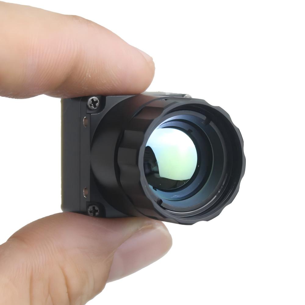
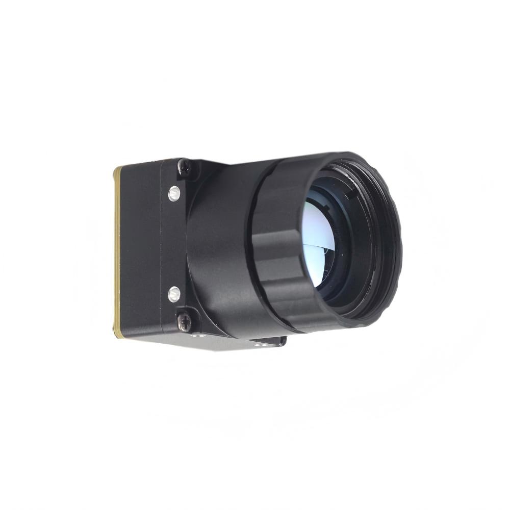
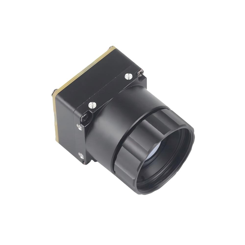
High Resolution Uncooled Infrared 1280*1024 Thermal Imaging LWIR Camera
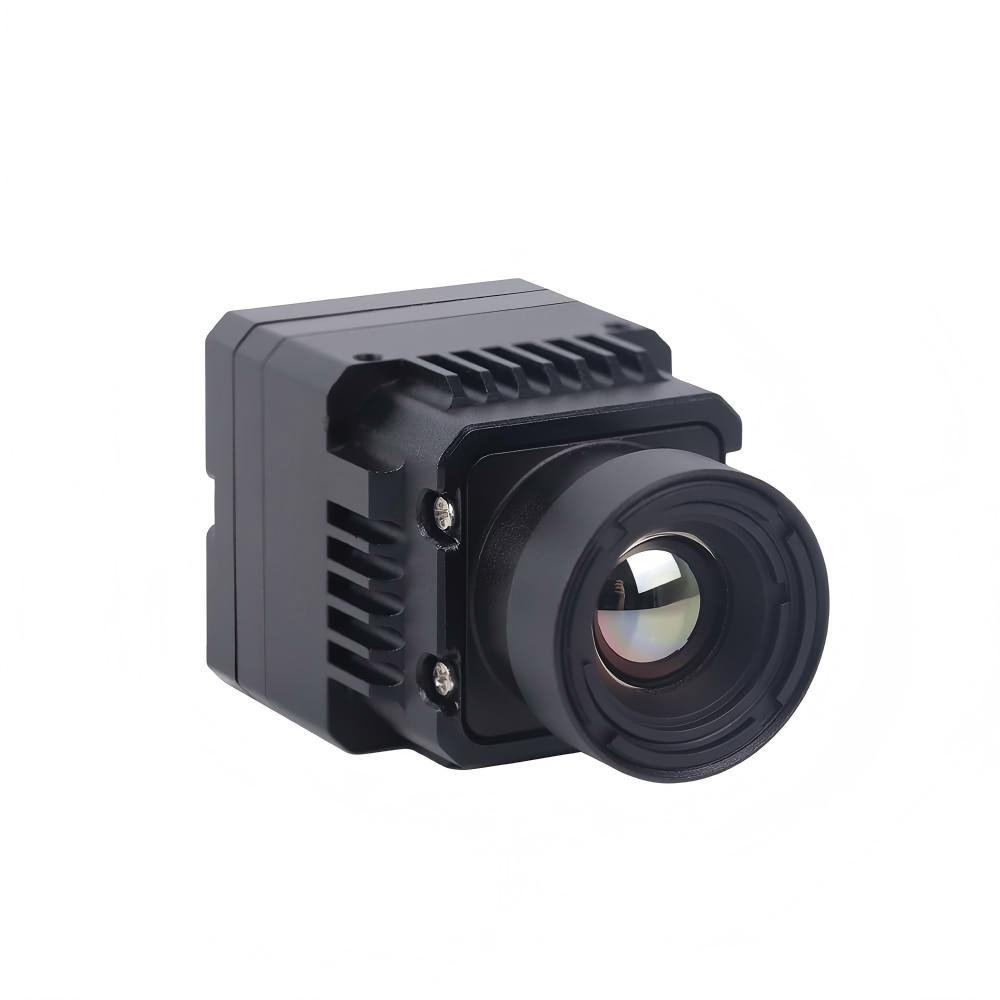
This flagship 1280x1024 thermal core represents the top tier of uncooled long-wave infrared performance. Built for counter-UAS systems, long-range border security installations, and heavy-lift UAV gimbals, it features a native SXGA VOx microbolometer array at a 12 μm pixel pitch. Paired with an athermalized 25mm f/1.0 Germanium lens assembly, this core resolves fine structural details at long tactical ranges where standard VGA sensors fail.
Key Technical Specifications:
- ⚙️ Focal Plane Array: 1280 x 1024 Native Uncooled VOx Microbolometer
- ⚙️ Pixel Pitch: 12 μm
- ⚙️ Spectral Range: 8 μm to 14 μm (LWIR)
- ⚙️ Thermal Sensitivity (NETD): ≤ 40 mK at f/1.0, 25°C
- ⚙️ Frame Rates: 25 Hz / 30 Hz / 50 Hz programmable output
- ⚙️ Optical Assembly: 25mm f/1.0 Athermalized Lens
- ⚙️ Digital Video Interfaces: 14-bit / 8-bit BT.656, Parallel, USB 3.0, HDMI
- ⚙️ Power Consumption: ≤ 2.2 W under steady-state operation
Uncooled Infrared RJ45 CVBS RTSP IP 640*512 Thermal Sensor Camera Module
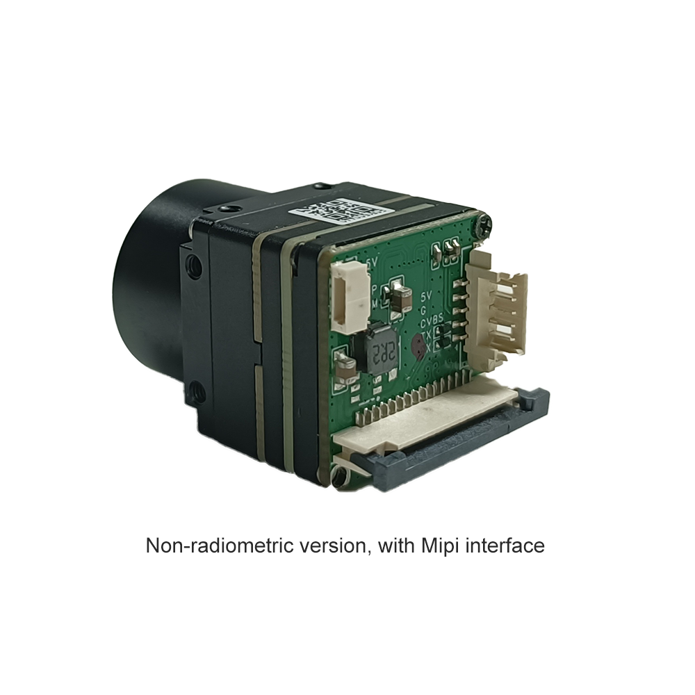
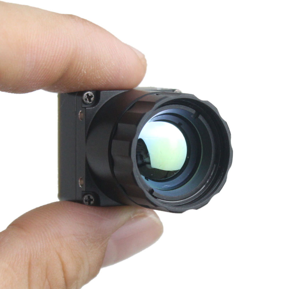
Engineered for compact tactical drones, perimeter IoT nodes, and weight-sensitive gimbals, this module uses a dedicated ASIC pipeline with native IP streaming. It outputs a 640x512 VGA stream with onboard H.264/H.265 compression, serving RTSP network video over an RJ45 Ethernet port alongside low-latency CVBS analog output. Its sub-30-gram footprint makes it ideal for fast integration where size and weight are hard constraints.
Key Technical Specifications:
- ⚙️ Focal Plane Array: 640 x 512 Uncooled VOx / ASIC Thermal Core
- ⚙️ Pixel Pitch: 12 μm
- ⚙️ Spectral Band: 8 μm to 14 μm
- ⚙️ Thermal Sensitivity (NETD): ≤ 40 mK at f/1.0
- ⚙️ Video Streaming: Direct RJ45 Ethernet (RTSP / ONVIF Profile S) + CVBS Analog
- ⚙️ On-Core Compression: Real-time hardware H.265 / H.264 encoding
- ⚙️ Mechanical Weight: ≤ 28 grams (core without lens)
- ⚙️ Input Voltage & Power: DC 3.7V - 5.0V, steady-state ≤ 1.2 W
6. ISP Pipeline, NUC Calibration & Hardware Interfaces
Consider the raw data throughput: a native 1280x1024 microbolometer outputting 14-bit digital radiometric data at 50 Hz generates a raw bitstream exceeding 917 Mbps. You cannot simply pipe that raw data straight to a display. It takes an advanced onboard Image Signal Processor (ISP) pipeline to clean, calibrate, and enhance the feed in real time before it reaches the physical output bus:
- ⚙️ Non-Uniformity Correction (NUC): Microbolometers suffer from unavoidable pixel-to-pixel responsivity variations and dark current drift. The NUC engine runs a two-point calibration (gain and offset) across every single pixel. Periodic single-point calibration uses an internal mechanical shutter, while modern systems utilize Scene-Based Non-Uniformity Correction (SBNUC) algorithms to eliminate fixed-pattern noise on the fly without locking up the video frame.
- ⚙️ Bad Pixel Replacement (BPR): Dead, saturated, or erratic bolometer pixels are identified during factory calibration and logged in non-volatile memory. At runtime, the BPR block dynamically reconstructs those coordinates by interpolating adjacent healthy pixel values.
- ⚙️ Temporal & Spatial 3D Noise Reduction (3D-DNR): High-resolution arrays run recursive multi-frame temporal filtering alongside spatial bilateral filtering. This strips out high-frequency Gaussian electronic noise without introducing ghosting or trailing behind fast-moving objects.
- ⚙️ Digital Detail Enhancement (DDE): The ISP performs multi-scale spatial frequency decomposition, separating the scene into low-frequency dynamic range data and high-frequency edge detail. The high-frequency layer is amplified and blended back into the image, pulling out fine physical edges on distant targets and terrain.
- ⚙️ Dynamic Range Compression & CLAHE: The microbolometer's wide 14-bit dynamic range (16,384 discrete levels) is mapped to standard 8-bit display palettes (256 levels) using Contrast-Limited Adaptive Histogram Equalization. This prevents scene washouts when hot elements (like rocket motors or turbine exhausts) enter a cold background.
Modern high-resolution modules support diverse hardware interfaces to suit different embedded host architectures. These include MIPI-CSI2 and Parallel LVDS for direct, low-latency interfacing with FPGA and SoC image ingest ports, USB3.0 (UVC) for rapid prototyping on edge platforms like NVIDIA Jetson and x86 architectures, and dedicated RJ45 Ethernet ports supporting real-time RTSP/H.265 video streaming for network-integrated surveillance installations.
7. Mission Architectures: UAV Gimbals, C-UAS & Substation Monitoring
Deploying a native 1280x1024 high-resolution thermal imaging core delivers concrete operational advantages across three major industrial and defense applications:
1. Multi-Rotor & Fixed-Wing Tactical UAV Gimbals
Aerial surveillance is dictated by acoustic limits and standoff distance. To stay quiet and avoid detection from the ground, the aircraft has to fly high. With a standard 640x512 payload, staying high means losing positive identification of personnel and vehicles. Upgrading to a native 1280x1024 12 μm core allows the drone to double its operational ceiling while preserving the exact same Ground Sampling Distance (GSD) and pixel coverage on target. The aircraft stays quiet, survivability goes up, and image clarity remains uncompromised.
2. Counter-UAS (C-UAS) Precision Acquisition
Tracking Class-1 micro-drones against cluttered backgrounds (skyline clutter, tree lines, or clouds) requires extreme spatial acuity. A small plastic or carbon-fiber drone has a tiny thermal signature, concentrated almost entirely in its small brushless motors and battery pack. A 1280x1024 thermal core provides the pixel density needed to lock onto motor hubs at ranges past 1.5 kilometers, feeding clean coordinate tracks straight into optical tracking loops or directional RF defeat systems.
3. Radiometric Utility Substation Monitoring
High-voltage utility yards require automated thermal monitoring of disconnect switches, busbar splices, transformer bushings, and cooling banks. Standard thermal cameras lack the resolution to measure small contact points from fixed perimeter poles, requiring dozens of cameras to cover a single yard. A native 1280x1024 radiometric core covers broad switchyard areas with fewer camera positions while reliably resolving sub-inch connection lugs from hundreds of feet away, catching overheating components long before catastrophic failure occurs.
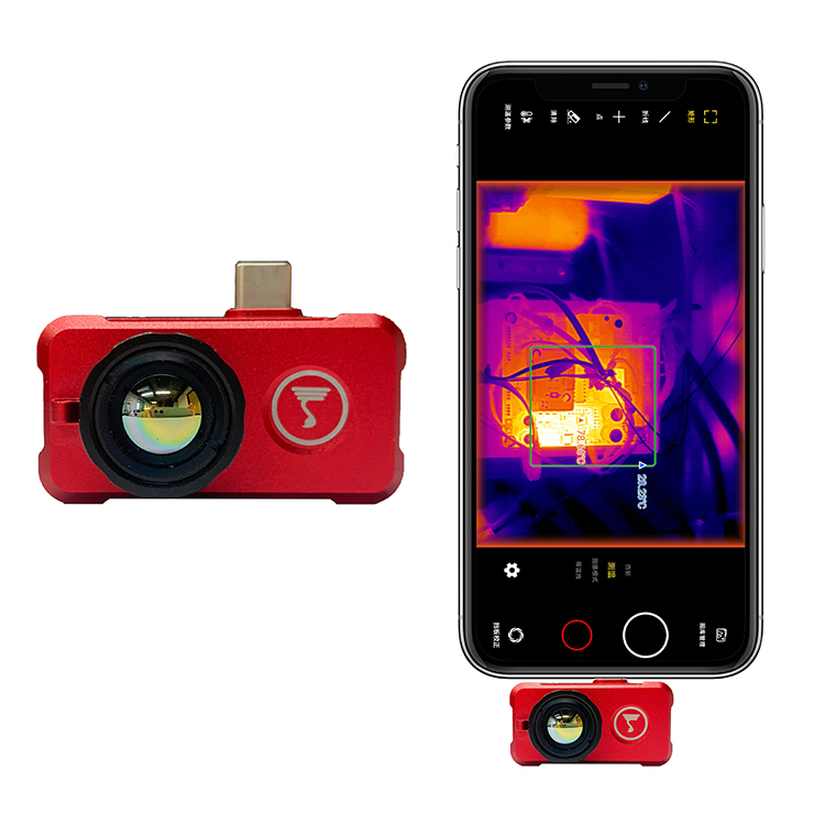
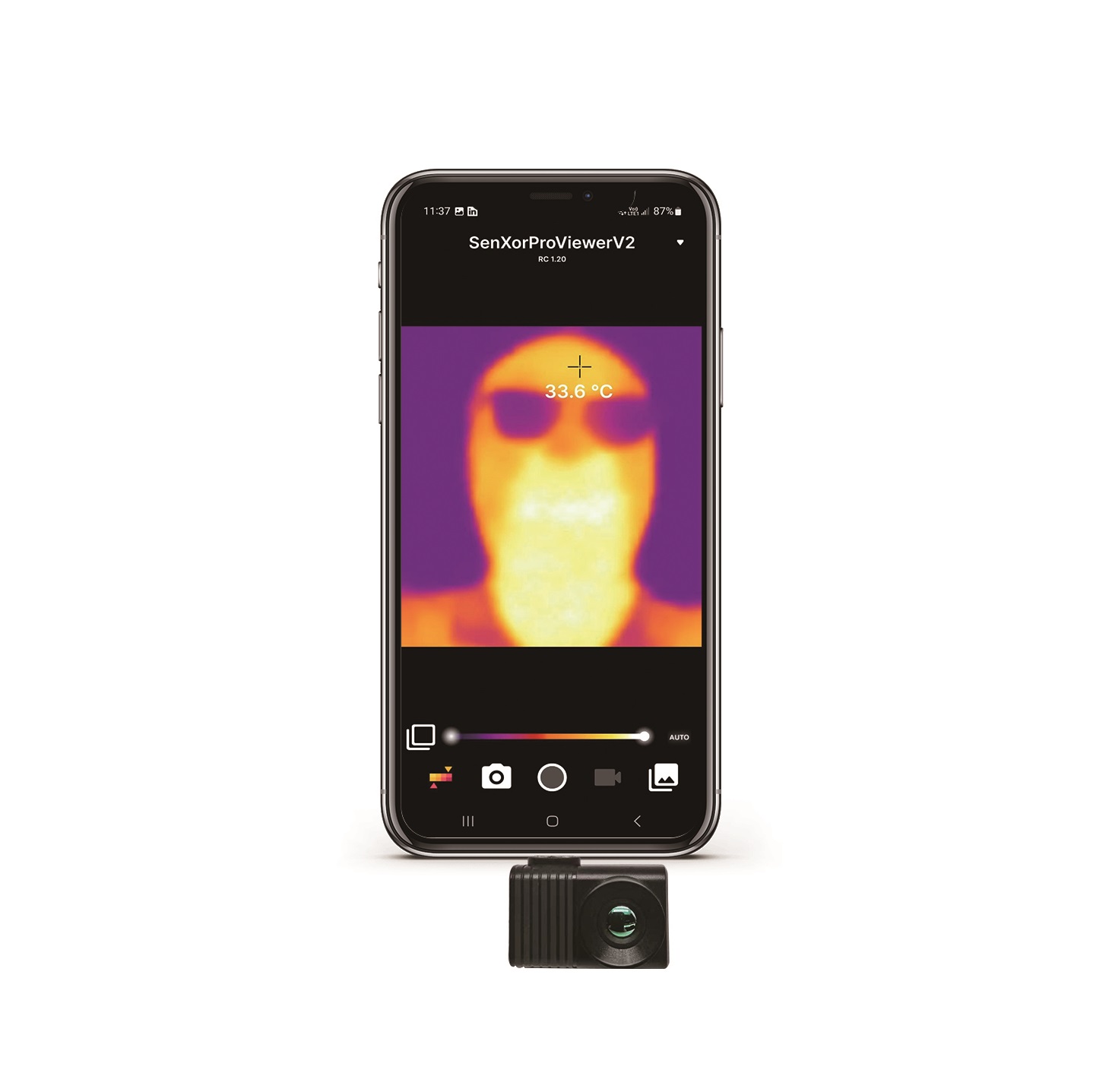
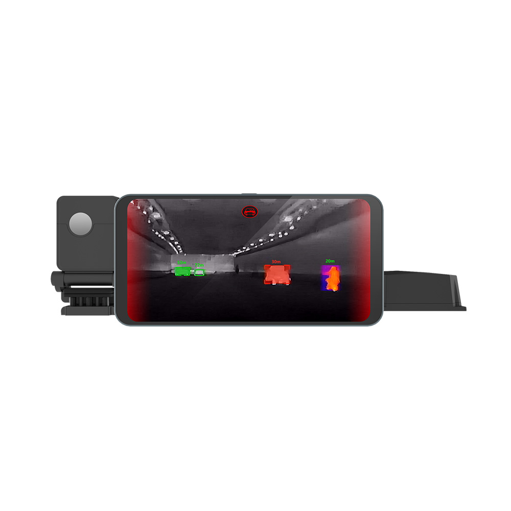
For more real-world deployment details, read our engineering guide on the 640x512 precision focus core implementation, and check out how portable thermal systems interface with field computers in our guide covering mobile-connected thermal imaging solutions.

8. Deep-Dive Frequently Asked Questions (FAQ)
What is considered 'high resolution' in thermal imaging compared to visible cameras?
Why upgrade from 640x512 to native 1280x1024 high resolution thermal cores?
How does high resolution improve Edge AI recognition and false-alarm rejection?
📚 References & Further Reading
- Industry Standard: Microbolometer Physics & Solid-State Detection — Wikipedia Microbolometer Overview
- Industry Standard: Thermographic Science & LWIR Principles — Wikipedia Infrared Thermography
- Related Guide: Embedded Hardware Integration for High-Res Thermal Cores — SPI & Parallel Interfacing for Embedded LWIR Modules
- Related Guide: Tactical Aerial Module Design & Architecture — 640x512 Precision Focus Core Implementation