

High Resolution Thermal Imaging: 1280x1024 LWIR Sensor Modules & OEM Solutions
2026年8月26日
Ultra-Low Power <0.5W Thermal Module for Drones & IoT | Compact OEM Cores
2026年8月27日
Low Power Consumption Thermal Camera Modules: Maximizing Efficiency for Drones & Edge AI
If you have spent any time bench-testing thermal payloads for small Unmanned Aerial Systems (UAS), battery-powered loitering munitions, autonomous field robotics, or remote Edge AI sensor stations, you already know the ugly truth: the infrared imaging core is almost always the component that breaks your SWaP-C (Size, Weight, Power, and Cost) budget. Payload engineers constantly hit a stubborn physical wall because high-performance infrared sensors have traditionally been absolute power hogs. That steady current draw does not just drain your battery packs—it wrecks flight endurance and creates an absolute nightmare for thermal management inside tight, sealed enclosures.
Here's the deal from a physics standpoint: uncooled Vanadium Oxide (VOx) and Amorphous Silicon (α-Si) microbolometer focal plane arrays (FPAs) are hypersensitive to internal, self-generated heat. When your core runs inefficient Readout Integrated Circuits (ROIC), sloppy power regulation, or power-hungry FPGAs, that wasted wattage turns directly into chassis heat. That internal temperature spike creates uneven thermal gradients across the sensor package, triggers fixed-pattern noise (FPN), accelerates calibration drift, and completely degrades your Noise Equivalent Temperature Difference (NETD). Achieving true low power consumption across long-wave infrared (LWIR) optics is not just about stretching battery life—it is an absolute requirement for getting clean thermal sensitivity, razor-sharp target detection, and rock-solid calibration in the field.
Table of Contents
- 👉 1. The Physics of Thermal Sensor Power: NETD Degradation, Parasitic Heat, and Uncooled VOx Bolometers
- 👉 2. Architectural Showdown: ASIC vs. FPGA vs. Generic Embedded SoCs for Infrared ISP
- 👉 3. Drone and UAS Integration: Maximizing Flight Durations via Sub-Watt Thermal Payloads
- 👉 4. Interface Protocols & Edge AI Pipelines: MIPI CSI-2, RJ45 IP, and RTSP Low-Power Architectures
- 👉 5. Firmware and Power Rail Strategies: Dynamic Voltage Scaling, Clock Gating, and Wake-on-Anomaly
- 👉 6. Industrial Product Comparison Matrix: Low-Power Thermal Camera Cores
- 👉 7. Deep-Dive Engineering FAQ
1. The Physics of Thermal Sensor Power: NETD Degradation, Parasitic Heat, and Uncooled VOx Bolometers
Uncooled Long-Wave Infrared (LWIR) detectors work in the 8 to 14 μm spectral window by absorbing radiant energy on microscopic suspended bridge structures etched directly over a silicon Readout Integrated Circuit (ROIC). Each tiny microbolometer pixel features an IR absorption layer, a vacuum-isolated thermal membrane, and a thermistor material—predominantly Vanadium Oxide (VOx)—that changes electrical resistance whenever incoming thermal radiation heats it up. In the shop, we measure this sensitivity using the Temperature Coefficient of Resistance (TCR):
TCR = (1 / R) × (dR / dT)
Because these microbolometers are designed to pick up minuscule thermal shifts down in the millikelvin range, the core's own thermodynamic baseline is everything. When an unoptimized thermal imaging engine burns 3W to 5W of power, that wasted electricity turns straight into heat inside the module housing. Stick that inside an IP67-rated airborne pod or a miniature drone gimbal with zero airflow, and that trapped heat has nowhere to go. The internal temperature climbs relentlessly.
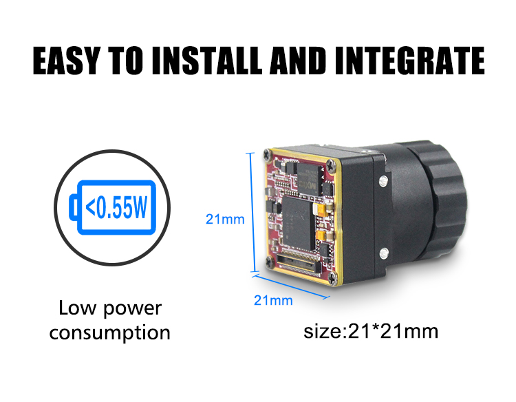
This parasitic thermal buildup creates two massive headaches for optical engineers:
⚙️ Non-Uniform Spatial Gradients: Heat sources on the digital processing board—like a hot switching regulator or an FPGA—are never perfectly centered behind the sensor. This creates an uneven temperature slope across the VOx detector array. Different regions of the sensor drift at completely different speeds. To stop the image from degrading into a muddy mess, the camera firmware has to constantly fire its mechanical shutter flag for Non-Uniformity Correction (NUC). That drops a shutter in front of the lens every few minutes, freezing your live video feed and breaking target lock on autonomous tracking pipelines.
⚙️ Johnson-Nyquist Thermal Noise Amplification: As the focal plane array gets hotter, fundamental electrical noise spikes. The primary culprit in microbolometers is Johnson-Nyquist thermal noise, defined by the standard voltage noise spectral density equation:
v_n = √(4 × k_B × T × R × Δf)
Where k_B is the Boltzmann constant, T is absolute temperature in Kelvin, R is the pixel resistance, and Δf is the electrical bandwidth. When parasitic heat pushes T upward, Johnson noise, 1/f flicker noise, and thermal fluctuation noise all increase in tandem. This degrades your true field NETD. A sensor rated at a razor-sharp ≤35 mK on a room-temperature test bench can easily blow out past >60 mK inside a hot payload housing. You end up with grainy fixed-pattern noise, washed-out contrast, and significantly reduced target detection range.
Designing clean thermal pathways that isolate this heat away from the sensor package takes serious engineering. These baseline thermal degradation behaviors are evaluated during standard qualification testing, following the exact same principles used in high-temperature and humidity environmental validation procedures to make sure optical payloads hold their calibration under harsh real-world conditions.
2. Architectural Showdown: ASIC vs. FPGA vs. Generic Embedded SoCs for Infrared ISP
The processing brain driving your microbolometer array dictates both the quality of your thermal imagery and your module's electrical efficiency. The raw data coming straight off an uncooled ROIC is rough, non-linear, and filled with pixel-to-pixel variations. The Image Signal Processor (ISP) has to crunch heavy math in real-time: blind-pixel interpolation, multi-point polynomial NUC, spatial-temporal 3D noise filtering (3D-DNR), dynamic detail enhancement (DDE), and radiometric temperature conversion at 25Hz to 60Hz without dropping frames.
In the past, engineers routinely used Field Programmable Gate Arrays (FPGAs) to handle this heavy pipeline. FPGAs make rapid firmware prototyping easy, but they are notorious power hogs. An FPGA relies on massive arrays of programmable logic blocks, lookup tables (LUTs), and reconfigurable routing switches powered by SRAM cells. You burn substantial current just toggling parasitic capacitance across all those universal interconnect lines, on top of static leakage current running across unused silicon gates. A mid-tier FPGA running a standard 640×512 50Hz thermal pipeline easily pulls between 2.5W and 4.5W just for the digital processing board.
Dedicated Application-Specific Integrated Circuits (ASICs) change the game entirely. In a purpose-built thermal ASIC, mathematical operations—like dead-pixel concealment and dynamic contrast mapping—are hardwired directly into silicon gates. Transistors only cycle when actual pixel data passes through the arithmetic logic units. By eliminating reconfigurable routing fabric and unused logic blocks, an ASIC cuts static leakage down to near-zero levels and slashes dynamic power draw.
| Architecture Metric | Dedicated Thermal ASIC | Mid-Tier FPGA (e.g., Artix-7 Class) | Generic Embedded ARM SoC + NPU |
|---|---|---|---|
| Typical Core Power (640×512 @ 50Hz) | 0.6W – 1.1W | 2.5W – 4.5W | 3.5W – 7.5W |
| Static Leakage Current | Ultra-Low (< 15 mA) | Moderate to High | High (Multi-core OS overhead) |
| Boot-to-First-Frame Time | < 2.5 seconds | 5.0 – 8.0 seconds | 12.0 – 30.0 seconds |
| Physical Footprint (Die & Package) | Ultra-Compact (< 10×10 mm) | Bulky (> 20×20 mm + Flash/RAM) | Large Complex Carrier Module |
| Thermal Dissipation Mechanism | Passive conduction via chassis | Dedicated aluminum heatsink | Forced-air or active heat pipe |
When you are designing tightly packaged hardware, migrating from an FPGA or generic ARM chip to a dedicated ASIC delivers an immediate 60% to 75% drop in total core power. That massive reduction in waste heat simplifies your mechanical design, as detailed in our architectural breakdown of miniaturized CMOS and thermal dual-spectrum sensors, proving that silicon-level optimization lets you strip out heavy copper spreaders and bulky cooling gear for good.
3. Drone and UAS Integration: Maximizing Flight Durations via Sub-Watt Thermal Payloads
On multirotor and fixed-wing tactical drones, total flight time comes down to a strict mass-energy balance. The flight endurance equation ($T_{\text{flight}}$) clearly demonstrates how payload electrical power and payload mass combine to penalize your battery capacity:
T_flight = (E_batt × η) / [ P_prop(M_frame + M_batt + M_payload) + P_avionics + P_payload ]
Where E_batt is your usable battery pack capacity, η is battery discharge efficiency, P_prop is the mechanical motor power required to lift total takeoff mass, and P_payload is the direct electrical draw from your sensors. An inefficient thermal payload hits this balance in three distinct ways:
⚙️ Direct Battery Drain: A legacy 3.5W thermal core draws continuous power that could otherwise feed flight avionics and RF data links. On micro-UAVs running small 1S or 2S LiPo packs (300mAh to 1200mAh), a single 3W sensor can burn up to 25% of the total onboard battery capacity on its own, severely shortening your mission loiter time.
⚙️ Indirect Mass Penalty: High heat output demands extra metal. A sensor core dumping 3W to 4W of thermal energy requires a solid aluminum thermal conduction block, external cooling fins, or ducting, adding 40g to 100g of dead weight to your gimbal assembly. In multirotor flight physics, every additional gram forces the brushless motors to spin faster, ramping up propulsion power consumption P_prop exponentially.
⚙️ Gimbal Stabilization Strain: Bulkier, heavier camera housings carry a higher moment of inertia. That forces you to use larger brushless gimbal motors with heavier stator windings, which draw significantly more holding current during high-speed maneuvers or when fighting wind shear.
Swapping in a sub-watt ASIC thermal module—like an ultra-compact MIPI core pulling under 0.8W—creates an immediate positive compound effect. You can eliminate heavy heatsinks, downsize to micro-brushless gimbal motors, and increase total aircraft flight duration by 12% to 25%. For tactical UAS and industrial airframes, integrating high-efficiency thermal payloads with modular aerial platforms engineered by enterprise developers like OBSETECH allows operators to maintain extended surveillance orbits without pushing airframes past their gross takeoff weight limits.
4. Interface Protocols & Edge AI Pipelines: MIPI CSI-2, RJ45 IP, and RTSP Low-Power Architectures
Once infrared radiation is captured and processed by the ISP, getting that data into your edge computing host represents another critical engineering choice. You have to match your interface protocol to your physical mounting space, cable length, and electrical power budget.
⚙️ Direct MIPI CSI-2 (Mobile Industry Processor Interface):
MIPI CSI-2 is the undisputed standard for low-power, short-run connections between an imaging sensor and an Edge AI application processor (such as NVIDIA Jetson Orin, Rockchip RK3588, or Raspberry Pi Compute Modules). MIPI uses Low-Voltage Differential Signaling (LVDS) with a physical swing of just 200mV to 400mV. Because the physical transceivers run at such low voltages, the entire interface consumes less than 80mW of power.
MIPI CSI-2 pipes uncompressed 14-bit or 16-bit raw radiometric frames directly into the host processor's Direct Memory Access (DMA) pipeline. This bypasses network stacks, decoders, and frame serialization latency, keeping host CPU utilization minimal. For embedded robotics and low-latency computer vision, developers routinely build around MIPI carrier boards and hardware ecosystems provided by Waveshare.
⚙️ Network IP Streaming (RJ45, RTSP, ONVIF):
When your thermal camera needs to feed directly into an industrial network switch, long cable runs, or digital wireless transmitters, network streaming is essential. An RJ45-enabled thermal camera integrates hardware H.264/H.265 video compression engines and an Ethernet Physical Layer (PHY) right on its interface board.
This onboard compression pipeline packages high-definition thermal telemetry into RTSP and ONVIF video streams. Running an Ethernet PHY and video compression chip adds 0.4W to 0.7W compared to a pure MIPI link, but it completely frees the host system from having to encode video. This allows direct integration into industrial monitoring setups, IP mesh radios, or cellular IoT gateways without needing a bulky companion computer.
⚙️ Legacy Analog Video (CVBS):
Analog Composite Video (CVBS) uses a simple onboard Digital-to-Analog Converter (DAC) to output standard NTSC or PAL video directly to analog FPV transmitters or legacy screens. Pulling just 100mW to 150mW, CVBS delivers near-zero latency with practically zero overhead, keeping it relevant for budget FPV platforms, loitering munitions, and straightforward thermal rifle scopes.
5. Firmware and Power Rail Strategies: Dynamic Voltage Scaling, Clock Gating, and Wake-on-Anomaly
Getting your sensor core down to absolute minimum power draw takes tight coordination across hardware design, power supply topology, and intelligent firmware control. Modern uncooled thermal cores use multi-tiered power management to eliminate parasitic drain at every opportunity.
⚙️ Dynamic Clock Gating (DCG) & Module Power Domains:
In modern ASIC designs, the internal ISP clock distribution network is actively managed. When your application only requests raw 14-bit data over MIPI, the core firmware shuts down clock lines to unused blocks—such as the pseudo-color look-up tables (LUT), on-screen display (OSD) overlays, and digital zoom engines. Power goes only to the active pixel pipe, cutting dynamic power losses by up to 30%.
⚙️ High-Efficiency Synchronous Switching Regulators:
Thermal cores require multiple internal voltage rails: 3.3V for analog ROIC biasing, 1.8V for I/O transceivers, and 0.9V to 1.1V for the digital core logic. Old-school thermal modules used inefficient Low Dropout (LDO) linear regulators, which simply burn off excess voltage as heat: P_loss = (V_in - V_out) × I_load. Modern low-power cores rely on high-frequency (>2.5MHz) synchronous buck regulators running at over 92% efficiency, paired with low-noise filtering stages to keep switching ripple out of sensitive analog bias circuits.
⚙️ Duty-Cycled Surveillance & Autonomous Threshold Interrupts:
For off-grid, solar-powered security outposts, wildlife monitoring stations, or remote pipeline inspection nodes, streaming full 50Hz video 24/7 wastes massive amounts of energy. Modern firmware supports smart duty-cycling and low-power standby modes:
- ✅ Deep Sleep Mode: Main ISP clocks are halted, the VOx bias voltage is cut, and the core drops into a sub-50mW sleep state while preserving its non-volatile calibration parameters in static RAM.
- ✅ Hardware Wake-on-Interrupt: The module wakes up in under 50 milliseconds via a simple external GPIO trigger connected to a low-power PIR sensor, radar unit, or tripwire.
- ✅ Autonomous Edge Analytics Trigger: Advanced ASIC cores can run internal radiometric checks at just 1Hz or 2Hz. The ASIC monitors target temperature values inside pre-set bounding boxes. If an object breaches the programmed temperature threshold, the module asserts a hardware interrupt pin, waking your host Edge AI computer (like a Jetson Orin) to run full classification and send an alert.
By offloading simple threshold monitoring to the low-power thermal sensor, your power-hungry companion computers can stay in deep sleep for 99% of their deployment life, dramatically extending field battery life.
6. Industrial Product Comparison Matrix: Low-Power Thermal Camera Cores
The technical matrix below details two production-grade thermal camera modules built specifically to hit strict SWaP-C requirements in airborne payloads, robotics, and industrial edge monitoring:
| Image | Product Model & Architecture | Resolution & Pixel Pitch | Video Interfaces | Power Draw | Key Features & Integration Scope | Direct Action |
|---|---|---|---|---|---|---|
|
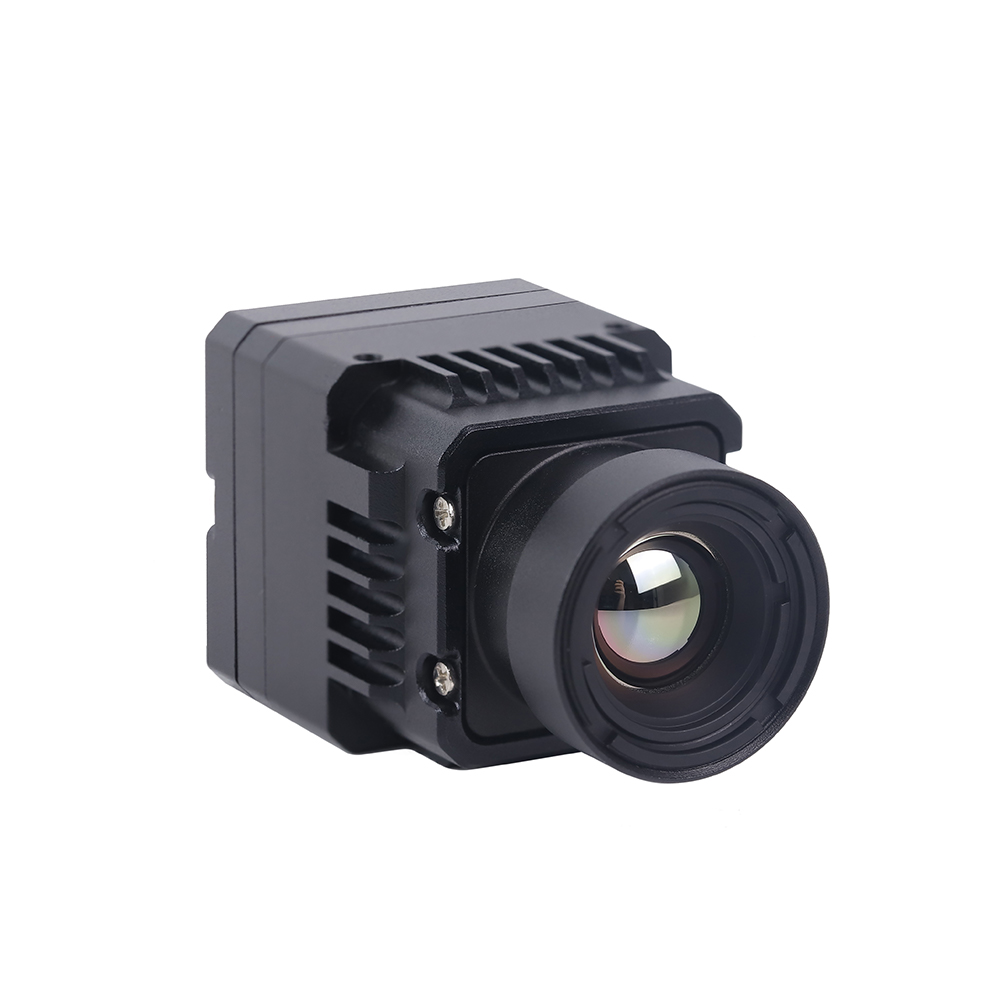
Uncooled Infrared RJ45 CVBS RTSP IP 640*512 Thermal Sensor Camera Module |
640×512 12μm Uncooled VOx |
RJ45 (Ethernet), RTSP, ONVIF, CVBS Analog | ≤ 1.2W (Full IP Stream) | Integrated ASIC network video processing, hardware dual-stream H.264/H.265 compression, autonomous web GUI configuration, compact airborne design. | View Specs |
|
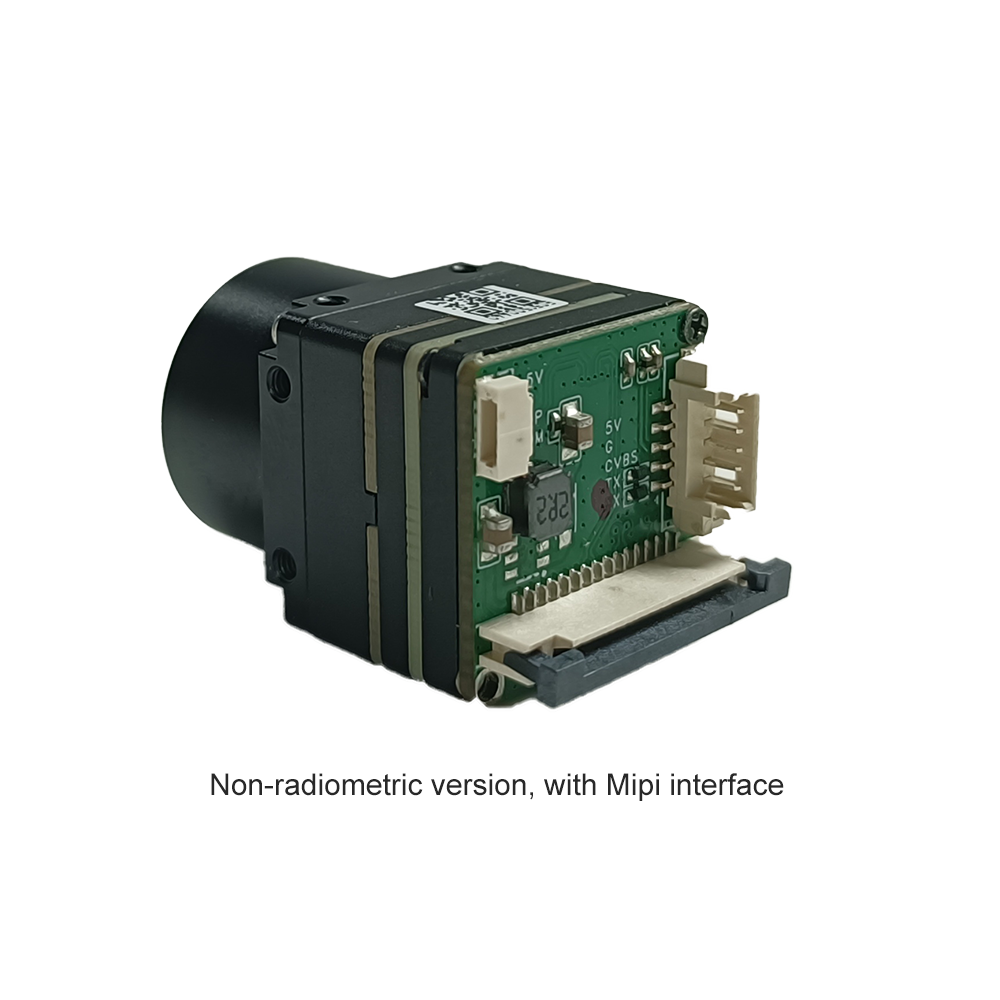
Uncooled Infrared MIPI Mini2 640/384/256 9mm Thermal Imaging Module |
640×512 / 384×288 / 256×192 12μm Uncooled VOx |
MIPI CSI-2 (4-Lane / 2-Lane), DVP Raw Data | ≤ 0.6W – 0.8W (Ultra-Low Power) | Direct-to-host raw radiometric output, ultra-low latency (<1 frame), zero network overhead, compact form factor designed for drone gimbals. | View Specs |
Spotlight: Uncooled Infrared RJ45 CVBS RTSP IP 640*512 Thermal Sensor Camera Module
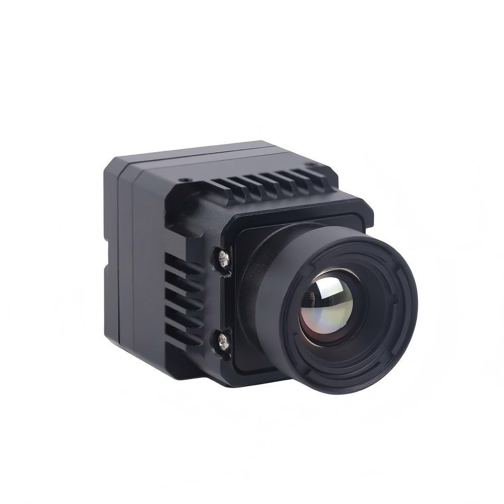
The Uncooled Infrared RJ45 CVBS RTSP IP 640*512 Thermal Sensor Camera Module is engineered for fixed monitoring points, perimeter security systems, and airborne IP network gimbals. By running on a hardened ASIC processing core, this module packs onboard H.264/H.265 video compression, an embedded web server, RTSP streaming, and a physical Ethernet PHY while pulling just ≤ 1.2W during full operation.
Built around a 12μm VOx microbolometer array with an NETD of ≤35mK, it delivers clean, high-contrast imagery with minimal spatial noise. Its dual-output design allows simultaneous low-latency analog CVBS output for local monitors alongside full-resolution IP video streaming for edge analytics, while its robust enclosure minimizes thermal drift under shifting ambient temperatures.
Spotlight: Uncooled Infrared MIPI Mini2 640/384/256 9mm Thermal Imaging Module
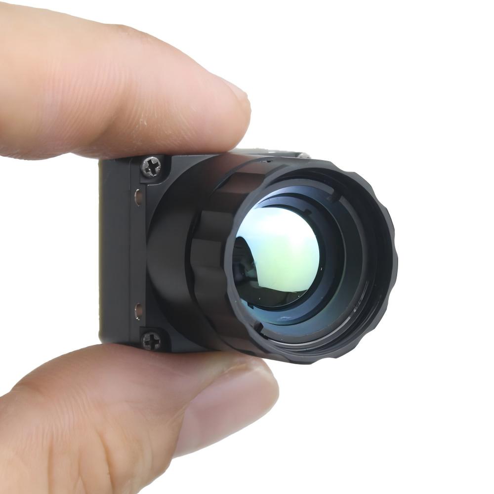
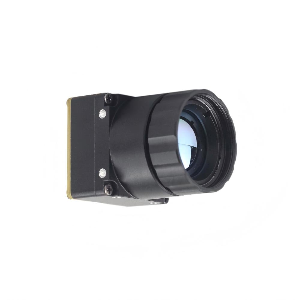
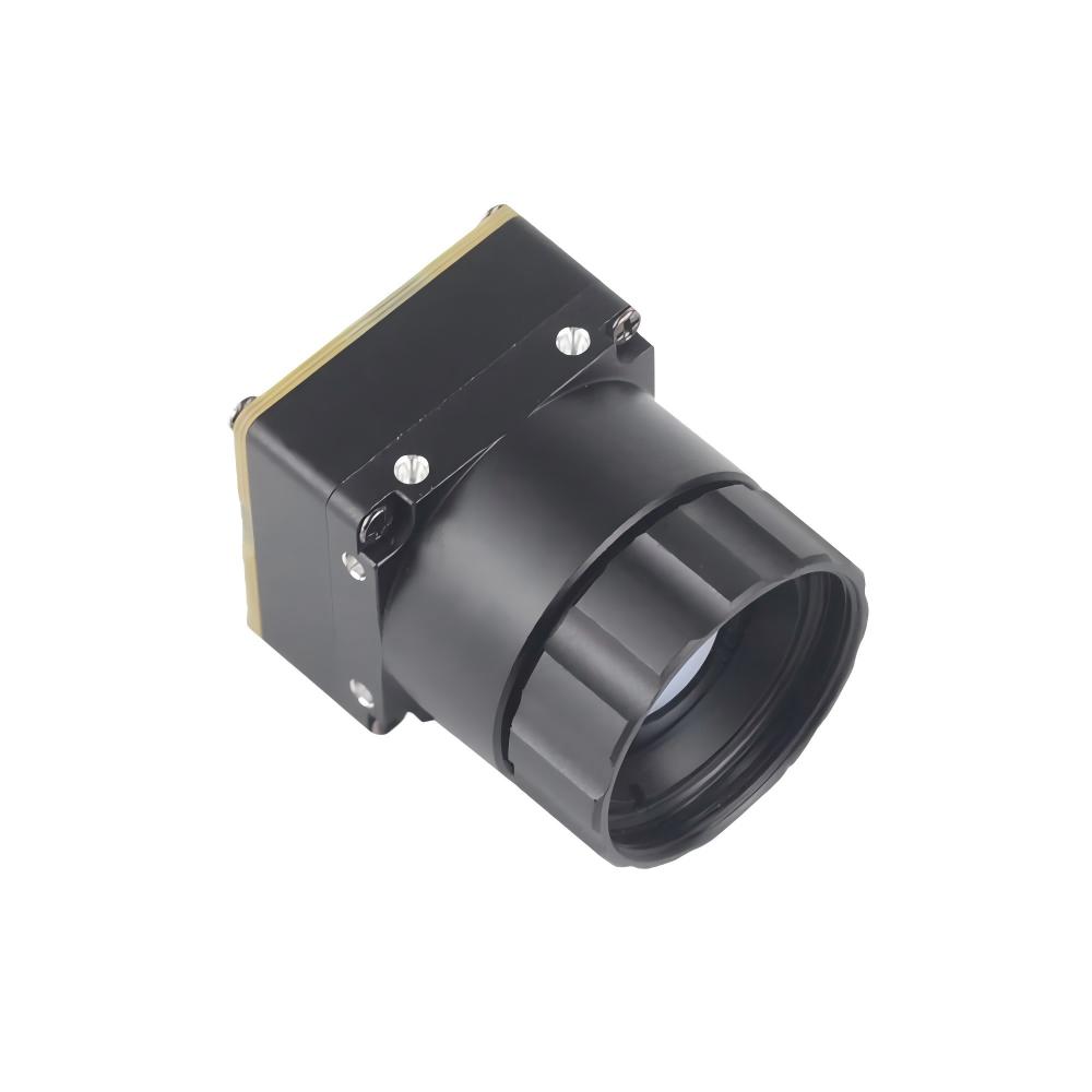
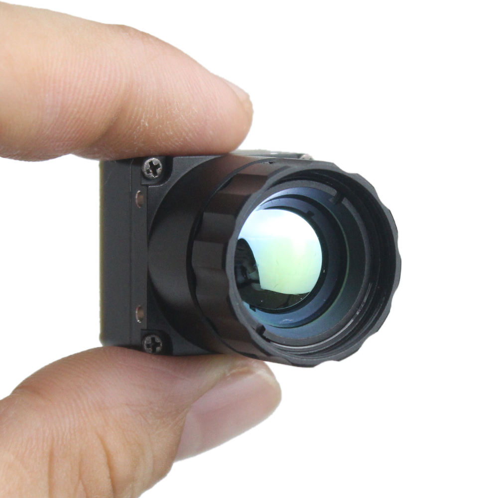
When you are building micro-gimbals or compact Edge AI platforms where every single gram and milliwatt matters, the Uncooled Infrared MIPI Mini2 640/384/256 9mm Thermal Imaging Module delivers exceptional SWaP-C efficiency. It eliminates the mass and power overhead of network transceivers by pushing raw digital thermal data directly across a high-speed MIPI CSI-2 interface.
Drawing just 0.6W to 0.8W during continuous 50Hz operation, the Mini2 delivers sharp detail with practically zero thermal dissipation. Its direct MIPI link feeds uncompressed 14-bit frames straight into host GPU/NPU memory, providing sub-frame latency object tracking, human detection, and automated target recognition on embedded platforms.
7. Deep-Dive Engineering FAQ
Why is low power consumption critical for uncooled thermal camera sensor fidelity?
How do dedicated thermal ASICs reduce power compared to FPGA-based image processing engines?
What architectural trade-offs exist between MIPI CSI-2 and RJ45 RTSP IP interfaces in edge deployments?
How do sub-watt thermal payloads directly extend flight durations in tactical drone platforms?
What firmware power-management modes are available for 24/7 off-grid thermal surveillance stations?
📚 References & Further Reading
- Industry Standard: Embedded developer resources and carrier board reference designs at Waveshare.
- Industry Standard: Enterprise tactical UAS airframes and drone payload integration by OBSETECH.
- Related Guide: Engineering qualification workflows for high-temperature and humidity environmental validation.
- Related Guide: Architectural teardowns of miniaturized dual-spectrum CMOS & thermal sensor cores.
- Related Guide: Core software integration principles via our embedded developer knowledge base.