
Top UVC Thermal Camera Modules for Linux, Pi & Embedded Systems
2026年7月21日
Best Long Range Thermal Camera Module for AI & Drone Integration: OEM/ODM Guide
2026年7月22日
CMOS Sensor Thermal Camera Module: Integration Guide & OEM Solutions
If you have spent any time in the shop designing automated surveillance systems, building rugged unmanned aerial vehicle (UAV) payloads, or mapping out advanced factory automation lines, you already know the score. Getting a compact, ultra-reliable thermal imaging camera integrated into a tight structural footprint is a massive challenge. Far too often, design engineers start searching for a CMOS sensor thermal camera module with the hope of mirroring the low-cost, high-speed performance of visible CMOS imagers, only to run headfirst into a brick wall of noise profiles, optical limits, and interface mismatches.
In modern optoelectronic system design, finding the sweet spot between resolution, pixel pitch, interface protocols (like MIPI CSI-2, USB 3.0, CVBS, or RJ45 RTSP), and thermal processing pipelines is what separates a world-class field device from a scrap-heap prototype. If you route your high-speed lines improperly, your thermal image looks like a snowy TV screen from 1985. If you pick the wrong lens coating, your sensitive detector is blinded by the first harsh storm in the field.
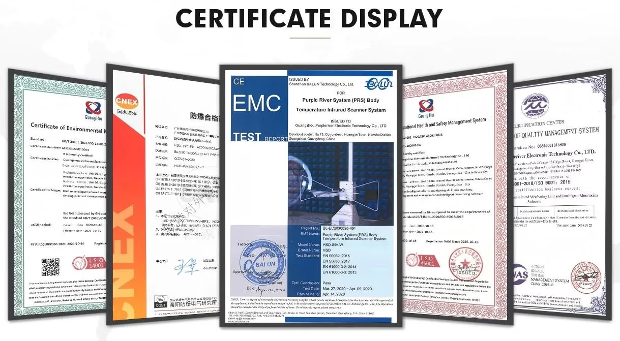
This engineering blueprint cuts through the marketing fluff. We will break down exactly how modern uncooled Long-Wave Infrared (LWIR) camera modules operate, examine the physical and electrical interfaces you will be dealing with on the bench, and introduce production-ready OEM modules designed by Purpleriver. Backed by a world-class engineering team drawing from the Hong Kong University of Science and Technology (HKUST) and former Huawei Hisilicon silicon-architects, these modules serve as a highly reliable starting point for mission-critical hardware deployments.
Table of Contents
- 👉 1. Technical Demarcation: Standard CMOS vs. Microbolometer ROIC
- 👉 2. Physical & Electrical Interfaces for Hardware Integration
- 👉 3. ASIC Processing Pipelines & Thermal Calibration
- 👉 4. Purpleriver OEM Thermal Sensor Camera Module Catalog
- 👉 5. Optical Engineering & Lens Selection for LWIR Cameras
- 👉 6. Exhaustive Deep-Dive FAQ (Technical Reference)
1. Technical Demarcation: Standard CMOS vs. Microbolometer ROIC
Let's get something straight right out of the gate: from a physics perspective, there is no such thing as a "standard visible CMOS sensor" that reads long-wave heat. When folks in the industry refer to a "CMOS sensor thermal camera module," they are actually talking about a highly complex hybrid device. They mean a specialized microbolometer thermal detector array constructed directly on top of, and structurally integrated with, a sub-micron CMOS Readout Integrated Circuit (ROIC).
To understand why this distinction is critical on the integration bench, consider the photoelectric differences. Standard visible-light CMOS sensors operate using the photoelectric effect within the visible and near-infrared (VNIR) bands (roughly 0.4μm to 1.0μm). Photons crash into an active silicon photodiode array, kicking electrons into a conduction band to generate an electrical charge that corresponds directly to visual brightness. Silicon is cheap, plentiful, and works beautifully in these bands.
But when you cross into the Long-Wave Infrared (LWIR) spectrum—the 8μm to 14μm band where terrestrial heat signatures sit—silicon becomes a brick wall. It is completely opaque. You cannot use standard photodiodes to catch these wavelengths. Instead, thermal camera modules use uncooled microbolometers, typically fabricated from Vanadium Oxide (VOx) or Amorphous Silicon (a-Si). If you want a deep dive into the underlying physics of thermal radiation, check out the Wikipedia Infrared Imaging guide.
Here is where the CMOS magic actually happens: each individual micro-bridge pixel in your thermal array is physically suspended over an underlying silicon CMOS wafer. This wafer acts as the ROIC. The structural, mechanical legs of the microbolometers are anchored to target metal pads on that underlying silicon chip. As incoming thermal radiation hits the suspended membrane, its physical temperature rises, shifting its electrical resistance. The micro-scale CMOS ROIC applies a highly precise, extremely low bias voltage across each pixel to measure these tiny shifts in resistance, integrating and multiplexing the raw voltage signals into a coherent analog stream before converting them on-chip to a clean digital output.
| Operating Parameter | Standard Visible CMOS Sensor | LWIR Thermal Sensor (with CMOS ROIC) |
|---|---|---|
| Spectral Band | 400 nm – 1000 nm (Visible / NIR) | 8,000 nm – 14,000 nm (LWIR) |
| Sensing Mechanism | Photovoltaic electron-hole pair generation | Bolometric resistance change via thermal absorption |
| Sensor Base Material | High-purity Monocrystalline Silicon | Vanadium Oxide (VOx) or Amorphous Silicon (a-Si) |
| Lens Elements | Optical Glass (Fused Silica, BK7) | Germanium (Ge), Chalcogenide glass, Silicon (Si) |
| Output Data Frame | 8/10/12-bit RAW Bayer pattern | 14-bit raw radiometric / digital count values |
| Pixel Architecture | Active Pixel Sensor (3T/4T phototransistor) | Suspended micro-bridge bolometer MEMS over ROIC |
2. Physical & Electrical Interfaces for Hardware Integration
When you are integrating one of these cores into your actual hardware, your choice of physical and electrical interface will make or break your design. This choice sets the rules for your physical board layout, dictates your power consumption, and controls pipeline latency. There is no one-size-fits-all here. It depends entirely on whether your module is going into a high-speed drone gimbal, a dusty factory floor, or an outdoor IP surveillance housing.
Here is how the main options stack up on the engineering bench:
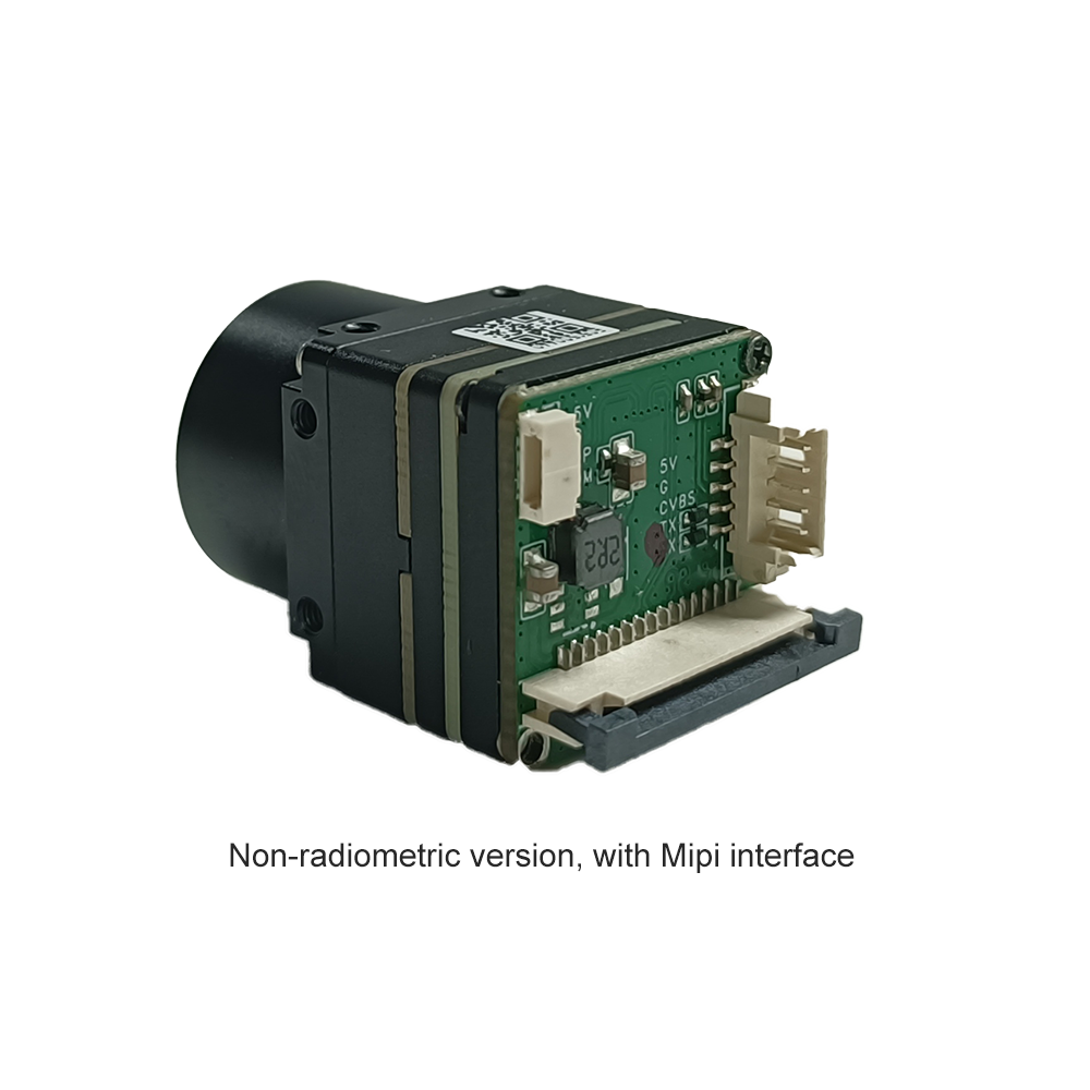
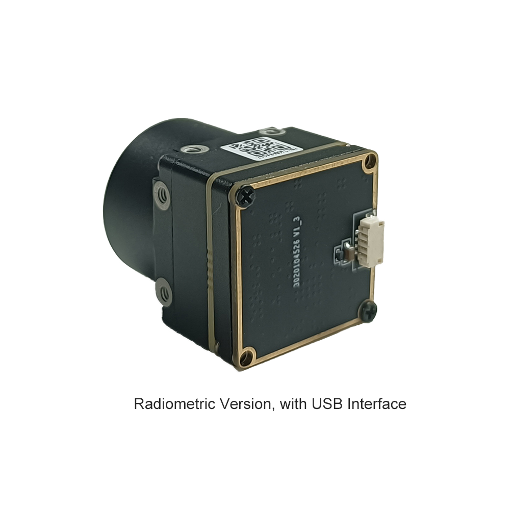
- 🔌 MIPI CSI-2 (Mobile Industry Processor Interface): If you are building deeply embedded systems running on System-on-Chip (SoC) architectures like the NVIDIA Jetson Nano/Orin, Rockchip, or Raspberry Pi, MIPI CSI-2 is your best friend. This protocol provides direct, high-bandwidth chip-to-chip communication over differential physical lanes (D-PHY). It sends uncompressed, raw 14-bit thermal video frames at lightning speed—usually under 5 milliseconds of hardware latency. But look out: since MIPI signals run at high frequencies, your PCB trace layout requires strict differential impedance control, targeting exactly 100 ohms. If you are routing signals through a rotating joint, like a drone gimbal, use high-spec micro-coaxial cable assemblies from specialized vendors like Micro Coaxial Cable Man to keep electromagnetic interference (EMI) from ruining your stream.
- 💻 USB (Universal Serial Bus): For plug-and-play prototyping or desktop configurations, USB 2.0 or USB 3.0 Type-C interfaces are incredibly convenient. Using standard USB Video Class (UVC) drivers, the thermal camera module presents itself to your OS as a basic webcam. You can instantly drag a processed 8-bit YUV or MJPEG video stream into your application without hacking the linux kernel or mess around with proprietary drivers. Better yet, high-end dual-mode modules can dump raw 14-bit radiometric data through an alternate endpoint, letting you run pixel-by-pixel temperature calculations on the host side.
- 📡 RJ45 Ethernet (IP / RTSP Network Streams): When you have to drop a monitoring node at the far end of an industrial yard, Ethernet is the only sensible choice. Onboard video encoding processors squeeze raw, bandwidth-heavy video frames into highly efficient, compressed streams using H.264 or H.265 codecs. The compressed feed is then served up over RTSP (Real-Time Streaming Protocol) or ONVIF profiles, fitting cleanly into existing security networks. If you are deploying compute-constrained nodes, take a look at how embedded architectures utilize these systems on SBCs by reviewing our breakdown of the thermal camera module for Raspberry Pi.
- 📺 CVBS (Composite Video Baseband Signal): Even in our digital-first world, legacy analog output (PAL or NTSC) is still a lifesaver. On commercial drone gimbals, FPV (First Person View) operators rely on single-coaxial analog RF transmitters because they degrade gracefully. If a digital link gets hit with interference, the screen freezes or goes black. With a CVBS link under heavy noise, you just get static—but you can still make out the horizon and save the drone from a costly crash.
3. ASIC Processing Pipelines & Thermal Calibration
Uncooled LWIR microbolometers are incredibly sensitive to their own internal temperature changes. If you attempt to display raw data straight out of the sensor, it looks like a noisy, non-uniform mess. Ambient heat from the camera's own processing chips, changing winds, or solar exposure on the casing causes the pixels to drift. To solve this, professional-grade modules run a dedicated ASIC processing pipeline that sits right behind the sensor. This ASIC performs a series of real-time spatial filtering and mathematical calibration steps before the video is packaged for the interface.
Here are the non-negotiable steps happening behind the scenes on a high-end thermal core:
⚙️ Non-Uniformity Correction (NUC): Every single pixel on a microbolometer wafer has a slightly different electrical resistance. As the ambient temperature shifts, these individual differences become obvious, creating spatial pattern distortion—otherwise known as fixed-pattern noise (FPN). The system fixes this by doing a One-Point Calibration (OPC), commonly known as a NUC. Every few minutes (or when the internal thermistor notices a temperature swing), a mechanical shutter drops in front of the lens to establish a flat temperature baseline. For critical industrial applications where you cannot afford a split-second video freeze (like automated closed-loop laser cutting), high-end modules run shutterless predictive algorithms that dynamically compensate for drift using internal thermodynamic models.
🛠️ Bad Pixel Replacement (BPR): Real-world microbolometer yields are rarely flawless; there are always a few dead or unstable "hot" pixels that do not track temperature changes. The ASIC maintains an internal flash-resident bad pixel map. By analyzing the 8-neighbor pixels in real time, the processor performs spatial interpolation (often a median filter) to drop a calculated value into the dead pixel's coordinates. This keeps the image clean and prevents false alarms in automated detection setups.
🎚️ Dynamic Range Compression & AGC (Automatic Gain Control): Raw radiometric data is delivered as a 14-bit signal (yielding 16,384 distinct gray values) to capture huge temperature sweeps (like -20°C to +150°C). Standard displays are limited to 8-bit inputs (256 gray values), and human eyes cannot detect subtle 14-bit shifts anyway. The ASIC runs complex Contrast Limited Adaptive Histogram Equalization (CLAHE) and digital AGC algorithms. It dynamically selects the active thermal window and maps those 16,384 values down to an optimized 8-bit image. This ensures a cold concrete wall and a warm human target in the same shot are displayed with high-contrast, razor-sharp edge definition.
4. Purpleriver OEM Thermal Sensor Camera Module Catalog
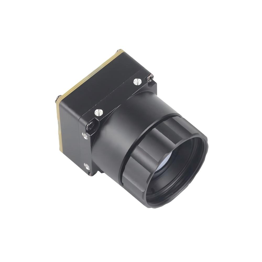
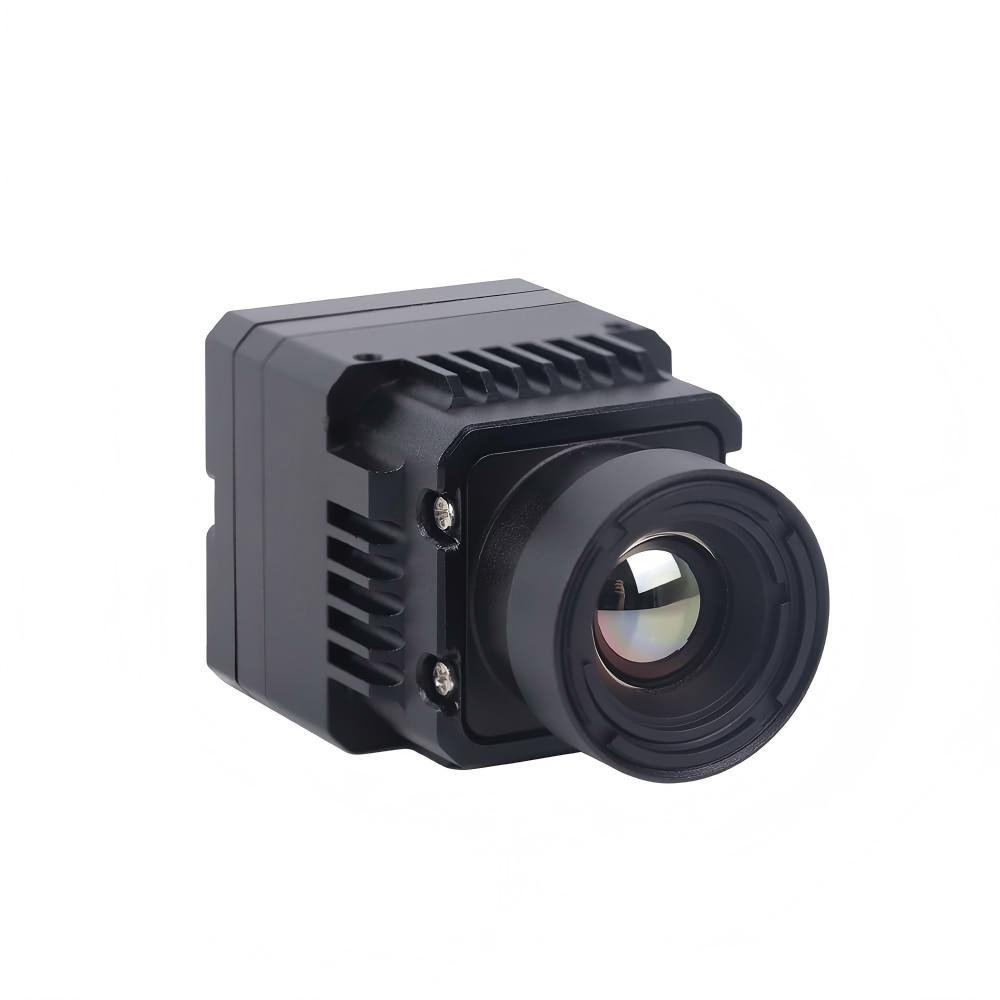
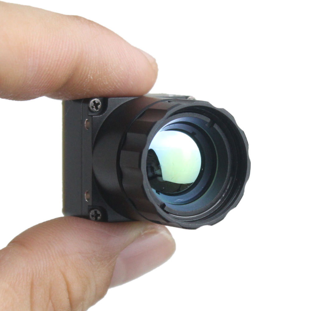
For industrial integrators, having a field-tested, highly customizable core makes all the difference when deadlines are looming. Purpleriver designs and builds high-spec, uncooled thermal cores tailored specifically for space-constrained, weight-sensitive, and low-power applications. Built by an elite engineering core tracing their roots directly to HKUST and Huawei Hisilicon silicon-architecture divisions, these modules deliver rugged, industrial-grade reliability where consumer-grade alternatives fail.
| Product Name & Description | Visual Product Profile | Key Engineering Specifications | Action |
|---|---|---|---|
|
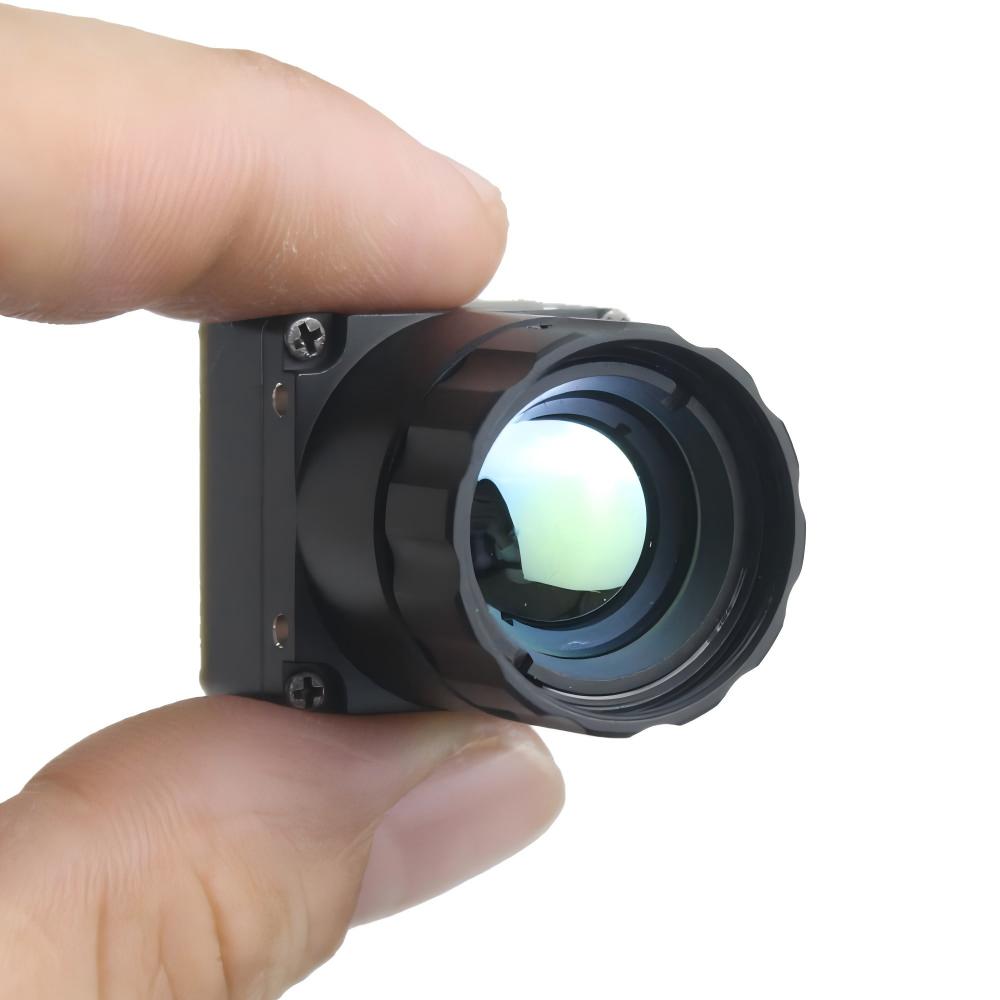
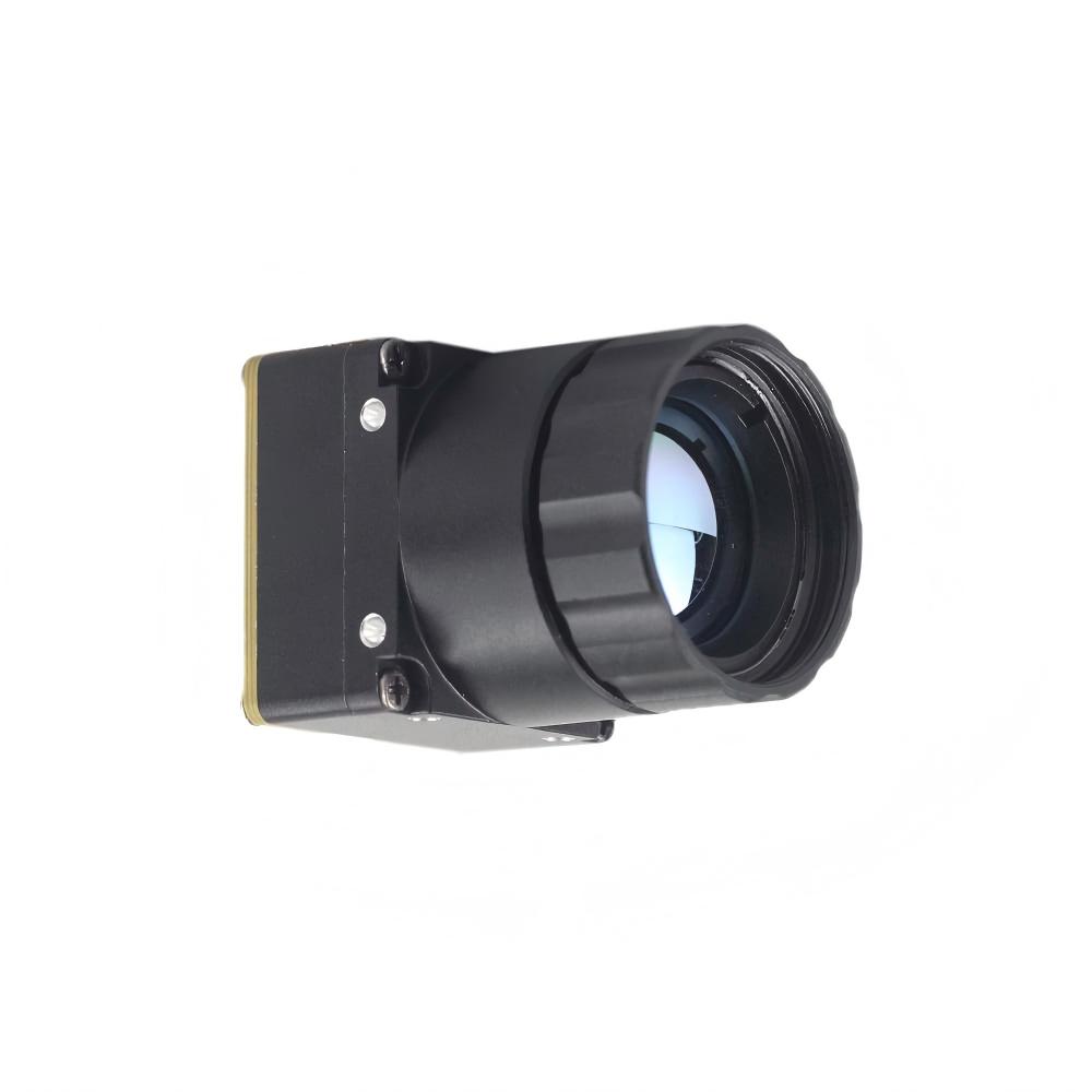
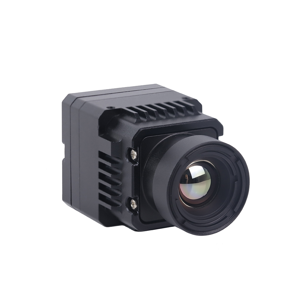
640*512 ASIC Thermal Sensor Module
Uncooled Infrared Mini 640*512 ASIC Thermal Imaging Camera Module For Drones. This module delivers high resolution and rich streaming versatility for professional payloads. |
|
|
Full Specs ➔ |
|
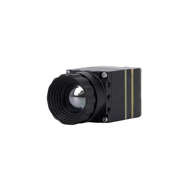
MD Series 384x288 Thermal Module
Purpleriver industrial-grade thermal imaging module designed for precision and rapid integration. Engineered for compact spaces and versatile connectivity. |
|
|
Full Specs ➔ |
Integration Guidelines for Purpleriver Cores
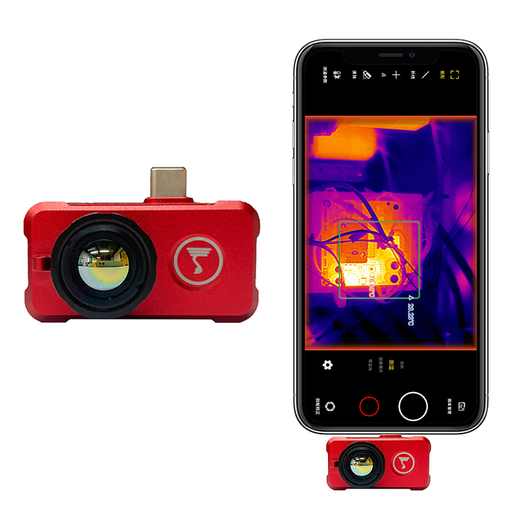
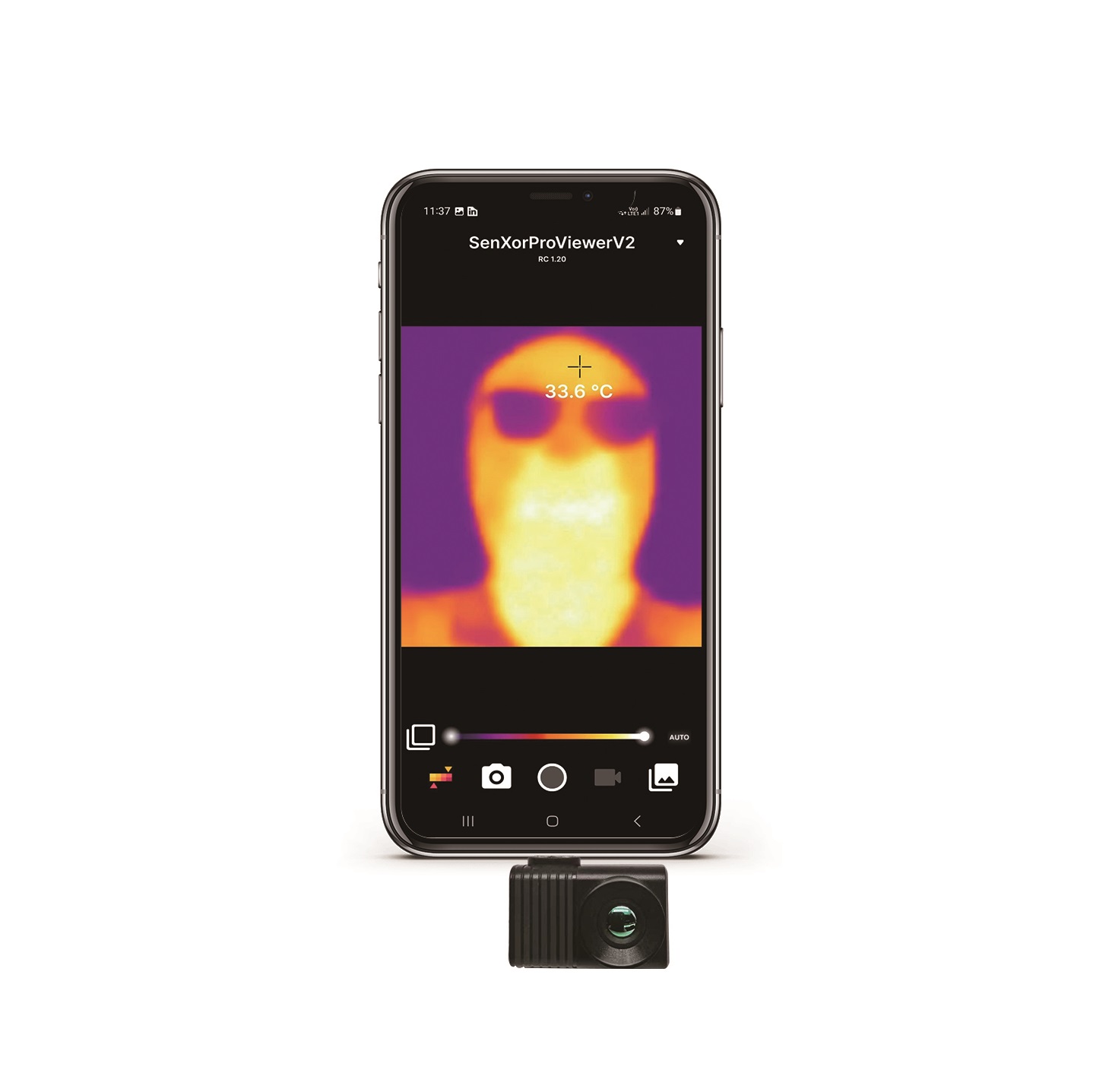
Deploying these versatile uncooled thermal modules enables product development teams to easily scale up production lines. These modules are built on core detector architectures identical to those found in premium uncooled infrared thermal imaging LWIR camera lines. For smaller-scale mobile integration requirements, evaluating how these core thermal architectures compare to ultra-compact, low-power layouts is straightforward. Review our specialized guide on selecting a smartphone thermal imaging camera module guidelines to learn more about balancing SWaP-C (Size, Weight, Power, and Cost) constraints.
View Product Details & Pricing ➔
5. Optical Engineering & Lens Selection for LWIR Cameras
Here is an optical reality check: you cannot run a thermal camera module through standard optical glass. Cheap quartz, silica, or BK7 glass acts like an opaque concrete wall to long-wave infrared energy. If you try it, you will just end up measuring the temperature of the back of your own lens. To pass the 8μm to 14μm spectral band, we have to look to specialized crystalline substrate materials.
When selecting your optical elements, pay close attention to these primary substrates:
- 💎 Germanium (Ge): This is the king of thermal materials. Germanium has an exceptionally high refractive index of roughly 4.0, which means you can design highly efficient, thin lenses with minimal optical aberration. It also has incredibly low dispersion qualities. But Germanium has a nasty Achilles' heel: thermal runaway. If your camera is deployed in a steel mill or in direct desert sun where the lens temp creeps past 60°C, Germanium’s absorption rate spikes exponentially. Eventually, the glass turns black to LWIR energy, and your image completely drops out.
- 🔬 Chalcogenide Glass: This is a synthetic chalcogen-based amorphous mixture (usually incorporating elements like selenium, arsenic, and sulfur). It is a fantastic option for automated, high-volume manufacturing because you can mold the lens under high heat rather than diamond-turning it. While its optical properties are slightly inferior to pure Germanium, it is much cheaper and thermal runaway is far less of an issue, making it a stellar option for industrial security setups.
- 🔍 Silicon (Si): While silicon works best in the Mid-Wave Infrared (MWIR) 3μm to 5μm band, thin-profile silicon element configurations can be designed to work reliably in low-cost, short-range LWIR applications. It is incredibly durable, abundant, and offers a tough, scratch-resistant surface.
Critical Optical Formulas
When calculating the physical limits of your system on the drawing board, keep these two fundamental optical formulas handy:
1. Instantaneous Field of View (iFOV)
$$iFOV = \frac{p}{f}$$
Where:
- 📌 iFOV: The spatial resolution of a single pixel in milliradians (mrad).
- 🎛️ p: The physical pixel pitch of the detector array (e.g., $12\mu\text{m} = 0.012\text{ mm}$).
- 📏 f: The effective focal length of the lens assembly in millimeters (mm).
Calculating the iFOV is critical—it tells you the absolute smallest physical feature size your sensor can resolve at a specific target distance.
2. Sensor Field of View (FOV)
$$FOV = 2 \cdot \arctan\left(\frac{W}{2f}\right)$$
Where:
- 🎚️ W: The total physical dimension of the sensor array width or height in millimeters ($W = N \times p$, where $N$ is the active pixel count along that axis).
- 📏 f: The focal length of the lens in millimeters.
Real-World Design Example
Say you are building a system around a 640x512 core with a 12μm pixel pitch ($0.012\text{ mm}$), and you pair it with a 19mm lens.
- First, find the physical width ($W$) of your sensor: $640 \text{ pixels} \times 0.012\text{ mm} = 7.68\text{ mm}$.
- Now, calculate the spatial resolution ($iFOV$): $\frac{0.012\text{ mm}}{19\text{ mm}} = 0.63\text{ mrad}$. That means at a distance of 100 meters in the field, a single pixel covers a square just 6.3 cm across ($0.63\text{ mrad} \times 100\text{ m}$).
- Next, calculate your horizontal field of view ($FOV$): $2 \cdot \arctan\left(\frac{7.68}{38}\right) = 2 \cdot \arctan(0.202) \approx 2 \cdot 11.43^\circ = 22.86^\circ$.
Lens Coatings
Because materials like Germanium have high refractive indices, reflections are brutal; untreated lenses reflect away almost 36% of incoming heat. To fix this, manufacturers apply deep anti-reflective (AR) coatings. For external-facing elements, engineers spec a rugged, Diamond-Like Carbon (DLC) coating. This ultra-hard barrier protects the expensive Germanium from high-speed sand scour, salty marine spray, and caustic petrochemical fumes on factory floors.
6. Exhaustive Deep-Dive FAQ (Technical Reference)
Can I interface a high-resolution CMOS/ROIC thermal sensor camera module directly with low-power microcontrollers like Arduino, or is a performance board like Raspberry Pi required?
What are the engineering differences between Vanadium Oxide (VOx) and Amorphous Silicon (a-Si) detectors in uncooled CMOS LWIR thermal modules?
What specific power supply noise isolation methods are required to prevent visual artifacts on a CMOS thermal sensor camera module?
📚 References & Further Reading
- Industry Standard: Learn more about external cable and signal integration from Micro Coaxial Cable Man.
- Scientific Baseline: Explore the technological history and physical theories of microbolometer structures at Wikipedia Infrared Imaging.
- Embedded Linux Platforms: Learn how to connect uncooled digital cores to SBC hardware in our guide on choosing a thermal camera module for Raspberry Pi.
- Mobile Form Factor Calibration: Read our handbook on choosing a smartphone thermal imaging camera module guidelines.
- Optoelectronic Cores: Deepen your understanding of large-format uncooled core assemblies by reading about uncooled infrared thermal imaging LWIR cameras.