
MIPI Thermal Camera Module: Low-Latency LWIR Integration for Drones & Edge AI
2026年9月16日
640x512 MIPI Thermal Module: High-Res OEM Camera Core for Drones & Embedded AI
2026年9月17日
MIPI Thermal Imaging Core: High-Res Embedded Vision for Drones & Edge AI
In modern embedded vision systems, the transition from legacy analog and bulk USB interfaces to native MIPI CSI-2 (Camera Serial Interface 2) represents an architectural leap for thermal imaging integration. Autonomous unmanned aerial vehicles (UAVs), tactical robotic payloads, and ruggedized edge AI processors demand deterministic low latency, minimal central processing unit (CPU) overhead, and stringent Size, Weight, Power, and Cost (SWaP-C) profiles. Integrating an uncooled long-wave infrared (LWIR) mipi thermal imaging core bypasses the latency-inducing bridge chips, high-overhead operating system USB host controller drivers, and cumbersome cabling that historically degraded real-time computer vision performance.
By routing high-bandwidth, 14-bit or 16-bit raw radiometric data directly into the host processor's Image Signal Processor (ISP) or heterogeneous System-on-Chip (SoC) memory via direct memory access (DMA), system architects unlock seamless sensor fusion, sub-frame target tracking, and high-frequency inference. Whether deploying thermal payloads for tactical inspection, perimeter defense, or search and rescue (SAR), pairing high-resolution vanadium oxide (VOx) microbolometer cores with native MIPI signaling establishes the technological foundation for modern edge autonomy.
Table of Contents
- 👉 1. The Architectural Advantage: Native MIPI CSI-2 vs. Legacy USB/SPI in Thermal Imaging
- 👉 2. Edge AI Acceleration: Zero-Copy Radiometric Processing & ISP Integration
- 👉 3. SWaP-C Optimization in Autonomous UAV Payloads & Gimbals
- 👉 4. Hardware Bring-Up: D-PHY Routing, V4L2 Drivers & FPGA Interfacing
- 👉 5. Commercial OEM Product Breakdown & Technical Comparison
- 👉 6. Deep-Dive Engineering FAQ
1. The Architectural Advantage: Native MIPI CSI-2 vs. Legacy USB/SPI in Thermal Imaging
Thermal imaging modules deployed in airborne robotics and tactical unmanned ground vehicles (UGVs) have historically relied on USB 2.0/3.0, Serial Peripheral Interface (SPI), or legacy analog composite (CVBS) connections. While functional for lab benchtop evaluations or slow-moving thermal telemetry monitoring, these interfaces introduce system bottlenecks when scaling up to high-resolution (640×512 or 1280×1024) uncooled long-wave infrared (LWIR) focal plane arrays (FPAs) operating at real-time 30 Hz to 60 Hz frame rates. In high-speed aerial autonomy and closed-loop visual inertial odometry (VIO), end-to-end transport latency directly dictates whether a platform successfully identifies an obstacle or collides with it.
Under a conventional USB 3.0 implementation, the microbolometer detector array converts incoming 8–14 μm infrared radiation into minute resistance changes across its pixel matrix. The Readout Integrated Circuit (ROIC) digitizes these analog signals via on-chip analog-to-digital converters (ADCs), outputting raw digital numbers. This bitstream is ingested by an onboard FPGA or application-specific integrated circuit (ASIC), conditioned, and pushed into a dedicated USB bridge controller (such as an Infineon/Cypress FX3 or FTDI bridge). The bridge chip packets the video into USB Video Class (UVC) or proprietary vendor bulk endpoints. Across the physical USB cable, data traverses host controller hardware (xHCI), triggering operating system interrupts that force the Linux kernel to schedule USB Request Blocks (URBs), reassemble packets in intermediate kernel buffers, and finally copy the frame into user-space RAM via context switches. This pipeline incurs a deterministic penalty: total end-to-end transport latency ranges between 15 and 45 milliseconds, while the host processor burns valuable CPU cycles managing interrupt service routines (ISRs).
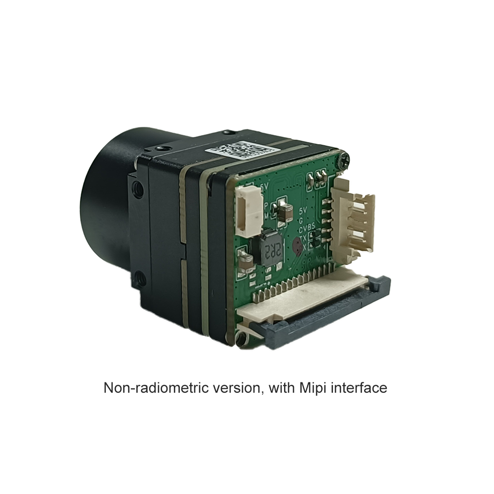
In contrast, an integrated mipi thermal imaging core communicates directly with the host System-on-Chip (SoC) via the MIPI CSI-2 protocol running over a high-speed D-PHY physical layer. The core routes differential serial data lanes directly from the thermal imaging engine into the host SoC's integrated CSI-2 receiver hardware. From this receiver, a dedicated hardware Direct Memory Access (DMA) engine channels uncompressed pixel data straight into system RAM, completely bypassing the primary CPU cores. There are no bridge chips, no USB endpoint packetizing overhead, and no OS interrupt storms. The end-to-end transport delay from the sensor array's bolometer readout integrated circuit (ROIC) to the SoC's unified memory ring buffer is reduced to sub-frame durations, routinely clocking in below 2 milliseconds.
From a transmission bandwidth standpoint, standard SPI connections fail when handling high-density radiometric arrays. Standard industrial SPI buses run safely between 10 MHz and 30 MHz. Streaming uncompressed 16-bit radiometric frames at 640×512 resolution generates:
$$\text{Bitrate} = 640 \times 512 \times 16\,\text{bits/pixel} \times 30\,\text{fps} = 157,286,400\,\text{bps} \approx 157.3\,\text{Mbps}$$
Standard synchronous SPI cannot service this payload without extreme spatial downsampling (e.g., dropping to 160×120) or throttling the temporal refresh rate to under 2 Hz, rendering the feed useless for airborne navigation or low-latency thermal tracking. Even Quad-SPI (QSPI) or Octal-SPI buses operating at high clock frequencies consume high pin counts while lacking the hardware-accelerated framing, packet metadata interleaving, and direct DMA deserialization native to modern SoC CSI-2 receiver blocks.
MIPI CSI-2 D-PHY interfaces resolve this bandwidth bottleneck through scalable differential data lanes. A single differential D-PHY lane operating at a modest 800 Mbps to 1.5 Gbps provides ample throughput. A standard dual-lane (2-lane) configuration comfortably yields 1.6 to 3.0 Gbps of raw bandwidth. This headroom allows a native MIPI LWIR core to transmit uncompressed 16-bit linear radiometric data at 60 Hz with substantial bandwidth to spare, enabling:
- ⚙️ Multi-Spectral Interleaving: Simultaneous frame-by-frame transmission of raw radiometric thermal data and synchronized visible-light channels over distinct Virtual Channel (VC) identifiers.
- ⚙️ Per-Frame Telemetry Embedding: Radiometric calibration coefficients, FPA core temperatures, shutter-state flags, and inertial measurement unit (IMU) time-sync tags injected directly into the vertical blanking intervals.
- ⚙️ Deterministic Line-Start Timing: Embedded line synchronization codes allowing sub-millisecond hardware triggers for closed-loop drone flight controllers and gimbal pan-tilt drivers.
Furthermore, native MIPI interfaces dramatically enhance electromagnetic compatibility (EMC) and mechanical reliability within tight aerospace housings. USB Type-C or Micro-B connectors introduce bulky, mechanically vulnerable interconnects susceptible to intermittent disconnects under high-vibration drone flight regimes or repetitive g-forces. MIPI CSI-2 cores utilize micro-pitch board-to-board connectors or locking Flexible Printed Circuit (FPC) ribbon cables, which weigh less than two grams and occupy a fraction of the physical volume. The low-voltage differential signaling (LVDS) scheme of MIPI D-PHY (typically ±200 mV differential swing in high-speed mode) generates negligible radiated emissions compared to high-power USB 3.0 transceivers, preventing EMI desensitization of adjacent GPS/GNSS receivers and ultra-high frequency (UHF) radio telemetry antennas. System designers interested in sensor selection strategies across varying integration environments should refer to the technical guide on choosing the right LWIR thermal camera module for edge systems.
2. Edge AI Acceleration: Zero-Copy Radiometric Processing & ISP Integration
In modern computer vision applications—such as autonomous loitering munitions tracking thermal centroids, automated perimeter intrusion detection, and industrial wildfire monitoring—the raw signal output must be converted into bounding boxes and spatial vectors with deterministic throughput. The computational efficiency of this pipeline hinges on how the incoming thermal data is ingested, structured, and presented to neural network accelerators, including Graphics Processing Units (GPUs) and Neural Processing Units (NPUs).
Native MIPI thermal cores allow for a true zero-copy processing architecture within unified memory embedded platforms, such as NVIDIA Jetson (Orin Nano, Orin NX, AGX Orin), Rockchip RK3588, or NXP i.MX8M series SoCs. When the camera core streams frames via CSI-2, the host SoC's internal Video Input (VI) subsystem decodes the packet headers and uses its hardware DMA channel to populate pre-allocated, physically contiguous memory blocks in DRAM. Operating within the Linux Video4Linux2 (V4L2) driver framework, these buffers are mapped using V4L2_MEMORY_MMAP or Direct Rendering Manager (DRM) DMA-buffers (DMA-BUF). Consequently, when an edge inference engine (such as NVIDIA TensorRT, OpenVINO, or RKNN) initiates an inference pass, the runtime engine points its execution tensor directly to the DMA-allocated physical memory address. Intermediate CPU memory copy calls (memcpy) are entirely eliminated from the capture loop. The host CPU load remains minimal, eliminating frame drops caused by system scheduling jitter.
A critical engineering consideration in thermal edge vision is determining whether to configure the core for 14-bit/16-bit linear radiometric output (raw Digital Numbers) or pre-processed 8-bit dynamic range output (such as YUV422 or greyscale RGB). Standard consumer infrared cameras process incoming radiometric sensor data through onboard DSP pipelines to yield an 8-bit display-ready image. This process employs Automatic Gain Control (AGC) algorithms, such as Contrast Limited Adaptive Histogram Equalization (CLAHE) or Digital Detail Enhancement (DDE). While 8-bit images are well-suited for human viewing on an operator ground control station (GCS), they present significant limitations for autonomous Edge AI perception.
When an onboard DSP compresses a 14-bit or 16-bit dynamic range down to an 8-bit scale (0–255 integer levels), subtle thermal gradients are permanently lost. If a high-temperature flare, hot exhaust duct, or structural fire enters the field of view, the global histogram shifts abruptly. This causes lower-temperature regions—such as a human hidden in foliage or a vehicle hidden in brush—to fall into completely uniform, black digital bins. Conversely, by utilizing a mipi thermal imaging core streaming raw 14-bit or 16-bit radiometric Y14 or Y16 frames directly over CSI-2, the downstream edge accelerator preserves absolute thermal values for every single pixel:
$$\text{Radiometric DN} \propto \int_{\lambda_1}^{\lambda_2} \epsilon(\lambda) \cdot L(\lambda, T) \cdot \tau_{atm}(\lambda) \cdot \tau_{opt}(\lambda) \, d\lambda$$
The raw digital number (DN) remains linear relative to the total received thermal radiance. Neural network models trained directly on high-bit-depth radiometric tensors can simultaneously detect human heat signatures in cold environments and track high-temperature exhaust plumes without saturating the input layers. The edge processor can split the incoming MIPI data stream into dual execution pathways:
- ✅ Operational Display Stream: One branch routes through a hardware-accelerated image signal processing pipeline (using platform VPU/GPU) to run real-time CLAHE and false-color palettes, outputting an optimized 8-bit H.264/H.265 video stream for the downlink telemetry link.
- ✅ Deep Learning Stream: The parallel branch feeds full-precision 14-bit or 16-bit linear radiometric tensors directly into the convolutional neural network (CNN) inference pipeline (e.g., YOLOv8-Thermal, RT-DETR) for absolute temperature thresholding and robust object classification.
To convert raw pixel values into true temperature readings ($T$ in Kelvin) on the edge host, the software pipeline applies the classical Planck calibration model using factory-calibrated radiometric metadata transmitted alongside the frame:
$$T = \frac{B}{\ln\left(\frac{R}{S_{\text{pix}} - O} + F\right)}$$
Where $S_{\text{pix}}$ represents the raw 14-bit/16-bit pixel digital number, and $R$, $B$, $F$, and $O$ are core-specific calibration constants derived during factory blackbody tuning. Processing this mathematical transform inside GPU CUDA kernels or NPU vector units yields dense, per-pixel temperature arrays at 60 Hz without burdening host CPU threads.
To support high-bandwidth sensor integration into advanced processing boards, aerospace engineers frequently source robust surface-mount components, interface transceivers, and edge processors through verified suppliers like JM Chip, guaranteeing signal fidelity from the raw imaging sensor to the inference core.
3. SWaP-C Optimization in Autonomous UAV Payloads & Gimbals
The design of miniature gimbal payloads for Class 1 and Class 2 Unmanned Aerial Systems (UAS) is governed by strict Size, Weight, Power, and Cost (SWaP-C) constraints. In multi-rotor and small fixed-wing platforms, every gram of payload weight imposes a non-linear operational penalty on flight duration, system balance, and battery capacity. Consequently, uncooled LWIR cores integrated into multi-sensor payloads must maximize electro-optical efficiency while maintaining minimal structural volume.
A major breakthrough in thermal miniaturization is the transition from legacy 17 μm pixel pitch microbolometers to 12 μm Vanadium Oxide (VOx) focal plane arrays (FPAs). The physical surface area of the sensor die scales with the square of the pixel pitch. Transitioning a 640×512 resolution detector array from 17 μm to 12 μm reduces the diagonal measurement of the active optical area from approximately 13.88 mm down to 9.83 mm. This substantial reduction in sensor footprint triggers an architectural cascade throughout the entire optomechanical assembly:
1. Optomechanical Volume and Lens Mass: In infrared optics, the focal length ($f$) required to achieve a target horizontal field of view (HFOV) is directly proportional to the sensor's physical width ($W$):
$$f = \frac{W}{2 \cdot \tan\left(\frac{\text{HFOV}}{2}\right)}$$
Because the 12 μm detector has a much smaller physical width ($W = 640 \times 12\,\mu\text{m} = 7.68\,\text{mm}$) compared to a 17 μm detector ($W = 640 \times 17\,\mu\text{m} = 10.88\,\text{mm}$), the required optical focal length to achieve the exact same field of view is approximately 29.4% shorter. Thermal imaging optics require precision-ground, anti-reflective coated Germanium (Ge), Chalcogenide glass, or Silicon elements, all of which exhibit high physical densities (Germanium has a density of approximately $5.323\,\text{g/cm}^3$). A shorter focal length combined with equivalent optical speed (such as $f/1.0$ or $f/1.1$) allows for dramatically smaller clear apertures and reduced optical element thicknesses. Consequently, the primary lens mass can be cut by 30% to 55%, reducing front-heavy overhang on gimbal payloads.
2. Gimbal Motor Sizing and Dynamic Response: The mass moment of inertia ($J$) of an optomechanical assembly around its center of rotation is calculated as:
$$J = \int r^2 \, dm \approx m \cdot r_{\text{gyr}}^2$$
Because inertia scales quadratically with the distance ($r$) from the rotation axis, pairing a compact, lightweight 12 μm lens assembly with an ultra-short 21 mm × 21 mm mipi thermal imaging core lowers the total moment of inertia by over 60% relative to older designs. Drone gimbal designers can replace heavy 28-series brushless gimbal motors with micro 18-series or 22-series motors without risking motor desync or stabilization drift during rapid high-G yaw maneuvers. The operational stabilization power falls from 5–8 Watts down to under 1.5 Watts, minimizing electromagnetic interference and system heat dissipation inside enclosed aerodynamic pods.
3. Thermal Core Electrical Power Budget: Modern native MIPI uncooled cores operate with steady-state electrical power consumption between 0.8W and 1.5W. Traditional cores with external interface boards often draw between 2.5W and 4W due to onboard power converters, microcontrollers, and interface translation ICs. Lower power consumption extends drone flight endurance while preventing thermal blooming within the gimbal enclosure. If a camera core releases excess heat inside a sealed dome, the resulting thermal radiation can reflect into the microbolometer, causing localized pixel saturation and degrading the Noise Equivalent Temperature Difference (NETD). Specialised payload integrators like OBSETECH utilize these lightweight, low-draw optoelectronic modules to engineer multi-axis electro-optical/infrared (EO/IR) surveillance gimbals for commercial inspection and tactical mapping drones.
4. Hardware Bring-Up: D-PHY Routing, V4L2 Drivers & FPGA Interfacing
Implementing a mipi thermal imaging core requires rigorous physical layer layout and kernel driver development. MIPI CSI-2 utilizes the D-PHY physical specification, which combines low-power (LP) single-ended signaling (0 to 1.2V) for control and link arbitration with high-speed (HS) low-voltage differential signaling (typically 100 to 300 mV) for data transmission. This hybrid signaling structure imposes strict PCB layout tolerances.
When routing high-speed differential pairs from the camera core's connector to the host SoC or FPGA, PCB layout engineers must enforce the following electrical constraints:
- ⚙️ Controlled Differential Impedance: Traces must be routed with a target differential impedance of $100\,\Omega \pm 10\%$ ($50\,\Omega \pm 10\%$ single-ended). Ground reference discontinuities must be strictly avoided.
- ⚙️ Intra-Pair Length Matching: The positive ($D_P$) and negative ($D_N$) lines within a given differential pair must be tightly length-matched to within $<0.15\,\text{mm}$ ($<6\,\text{mils}$), which equates to approximately 1 picosecond of differential skew. Excessive intra-pair skew converts differential energy into common-mode noise, which can corrupt data packets and degrade nearby RF receiver links.
- ⚙️ Inter-Lane Skew Control: The clock differential pair ($CLK_P / CLK_N$) and all associated data differential pairs ($D0_P/N$, $D1_P/N$) must remain length-matched within $<0.5\,\text{mm}$ ($<20\,\text{mils}$) to ensure proper setup and hold times across the receiver deserializer.
- ⚙️ Continuous Return Path: Never route high-speed MIPI traces across power plane splits or ground voids. When switching layers through vias, place dedicated ground stitching vias immediately adjacent to the signal vias ($<0.5\,\text{mm}$ center-to-center) to provide an uninterrupted path for high-frequency return currents.
- ⚙️ ESD Protection Diode Selection: If transient voltage suppression (TVS) diodes are installed for field reliability, select ultra-low capacitance arrays ($C_{\text{io}} < 0.2\,\text{pF}$) to prevent attenuation of high-frequency D-PHY signal harmonics.
On the software and firmware layer, integrating the thermal sensor into an embedded Linux environment involves configuring the Open Firmware Device Tree (DTS) and writing or adapting a Video4Linux2 (V4L2) kernel sub-device driver. Below is an example device tree node configuring a dual-lane MIPI thermal core connected to an embedded SoC's I2C control bus and CSI-2 receiver port:
&i2c3 {
    status = "okay";
    clock-frequency = <400000>;
    #address-cells = <1>;
    #size-cells = <0>;

    thermal_cam: thermal-core@1a {
        compatible = "purpleriver,mipi-lwir-core";
        reg = <0x1a>;
        clocks = <&cru CLK_MIPICSI_2CH_OUT>;
        clock-names = "xvclk";

        pinctrl-names = "default";
        pinctrl-0 = <&thermal_rst_gpio &thermal_pwr_gpio>;
        reset-gpios = <&gpio2 14 GPIO_ACTIVE_LOW>;
        power-gpios = <&gpio2 15 GPIO_ACTIVE_HIGH>;

        port {
            thermal_to_csi: endpoint {
                remote-endpoint = <&csi_in_endpoint>;
                data-lanes = <1 2>;
                clock-lanes = <0>;
                clock-noncontinuous;
                link-frequencies = /bits/ 64 <400000000>;
            };
        };
    };
};
The Linux kernel V4L2 driver handles sensor initialization, control configuration via I2C (or SPI), and format negotiation. Modern Linux kernels (5.x and 6.x) manage complex multimedia capture architectures through the Media Controller framework. Once the module registers with the kernel, you can inspect and configure the sub-device pipeline using standard Linux user-space utilities:
# Enumerate media controller topology and verify endpoint binding
media-ctl -d /dev/media0 -p

# Route the thermal core sub-device directly to the SoC video stream entity
media-ctl -d /dev/media0 -l '"purpleriver,mipi-lwir-core":0 -> "csi-receiver":0 [1]'

# Configure the pipeline format for 640x512 resolution using 16-bit linear radiometric output
media-ctl -d /dev/media0 -V '"purpleriver,mipi-lwir-core":0 [fmt:Y16_1X16/640x512 field:none]'
media-ctl -d /dev/media0 -V '"csi-receiver":0 [fmt:Y16_1X16/640x512 field:none]'

# Set video device capture format and capture a raw radiometric stream test frame
v4l2-ctl -d /dev/video0 --set-fmt-video=width=640,height=512,pixelformat=Y16\
v4l2-ctl -d /dev/video0 --stream-mmap --stream-count=1 --stream-to=radiometric_test.raw
When high-speed FPGA processing is required—such as in low-latency hardware tracking pipelines or custom multi-spectral fusion arrays—the MIPI CSI-2 stream can be routed into an FPGA fabric (e.g., AMD Xilinx Zynq UltraScale+ or Intel Cyclone V SoC). In these setups, a hard-macro or soft-core MIPI CSI-2 RX Subsystem decodes packet headers, performs byte-to-pixel lane unpacking, and routes raw pixel data over an AXI4-Stream bus directly into custom non-uniformity correction (NUC), bad-pixel replacement (BPR), and spatial filtering hardware blocks.
For large-format imaging arrays requiring extended bandwidth, developers can explore the design architecture used in next-generation 1280x1024 thermal modules. Additional design considerations for 640×512 and smaller arrays are covered in the technical overview of uncooled MIPI 640/384 9mm system integration.
5. Commercial OEM Product Breakdown & Technical Comparison
System integrators and optical engineers must balance form factor, lens options, thermal sensitivity (NETD), and interface protocols when choosing an infrared module. Below is a detailed technical evaluation of two industrial-grade thermal imaging cores manufactured by Purpleriver, engineered specifically for SWaP-constrained drone payloads and autonomous edge robotics.
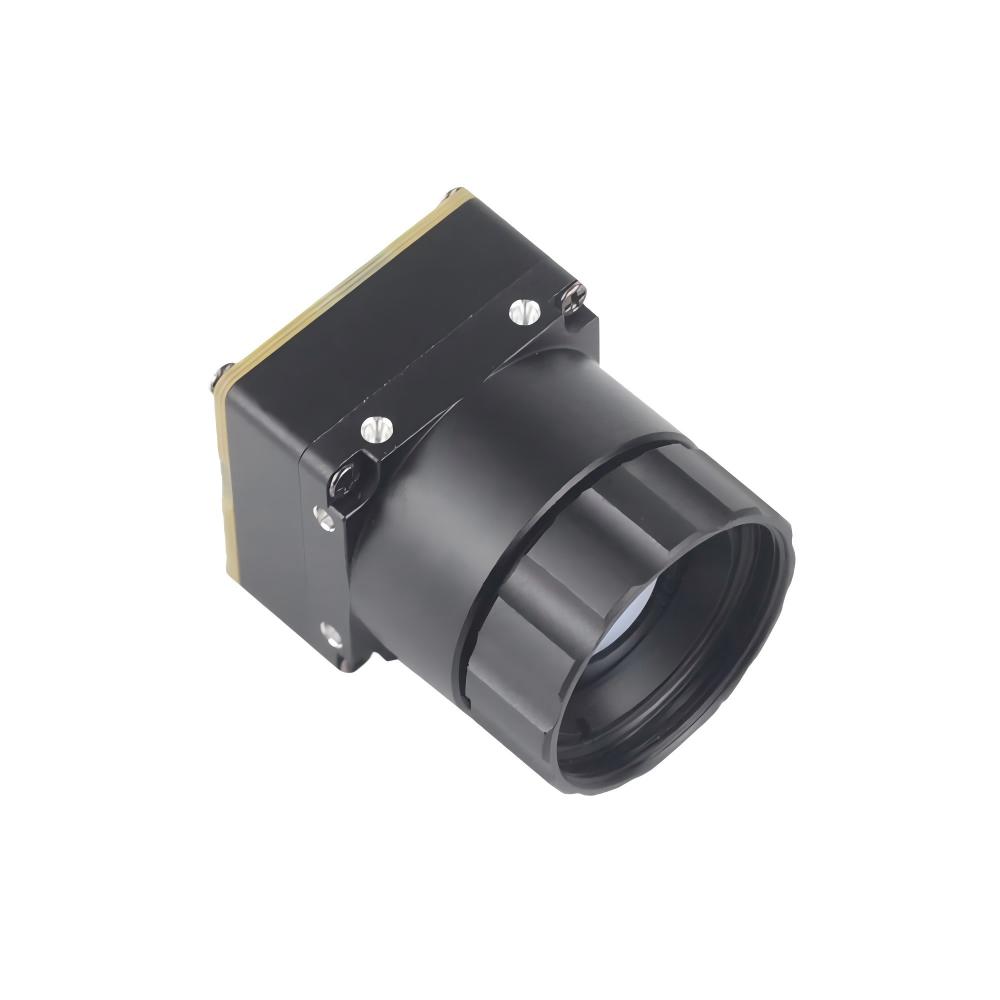
Uncooled Infrared Mipi 640 384 256 9mm Thermal Imaging Camera Module For Drones
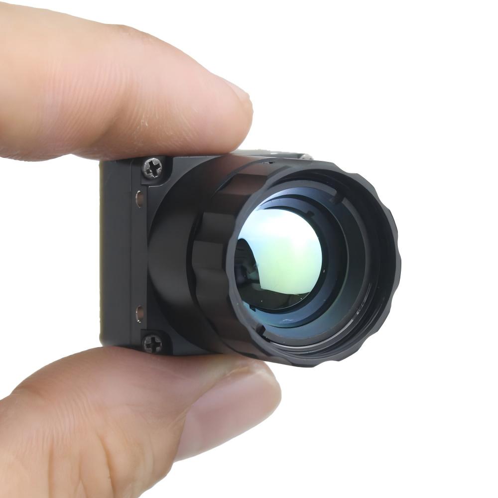
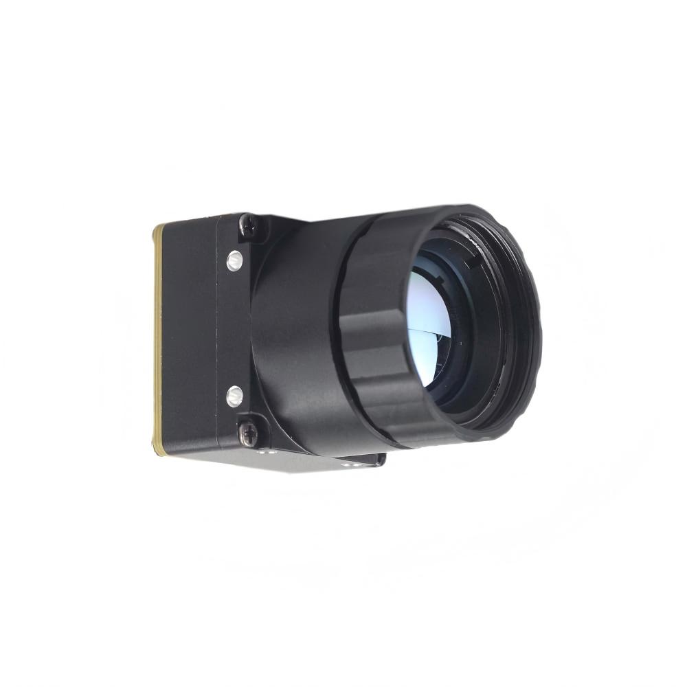
The Mini2 thermal module provides an ultra-compact footprint designed for direct embedded integration. Utilizing an uncooled Vanadium Oxide (VOx) focal plane array, this core delivers high-definition thermal imaging with low thermal latency. It is optimized for multi-rotor commercial drones, loitering platforms, and compact handheld inspection systems where every gram of weight affects flight endurance.
- ✅ Native Digital Interface: Low-profile MIPI CSI-2 interface for direct connection to host SoCs.
- ✅ Resolution Flexibility: Native 640×512 configuration, with optional 384×288 and 256×192 configurations.
- ✅ Standard Optics: Integrated 9mm athermalized lens providing a balanced field of view for aerial navigation.
- ✅ Form Factor Advantage: Engineered for tight structural envelopes and micro-gimbals.
| Detector Array Type | Uncooled Vanadium Oxide (VOx) Microbolometer |
| Resolution Options | 640×512, 384×288, 256×192 |
| Pixel Pitch | 12 μm |
| Optical Configuration | 9 mm standard athermalized infrared lens |
| Electrical Output | Native MIPI CSI-2 Raw / YUV Stream |
| Primary Feature Set | High-contrast image delivery, ultra-compact profile, minimal SWaP-C overhead |
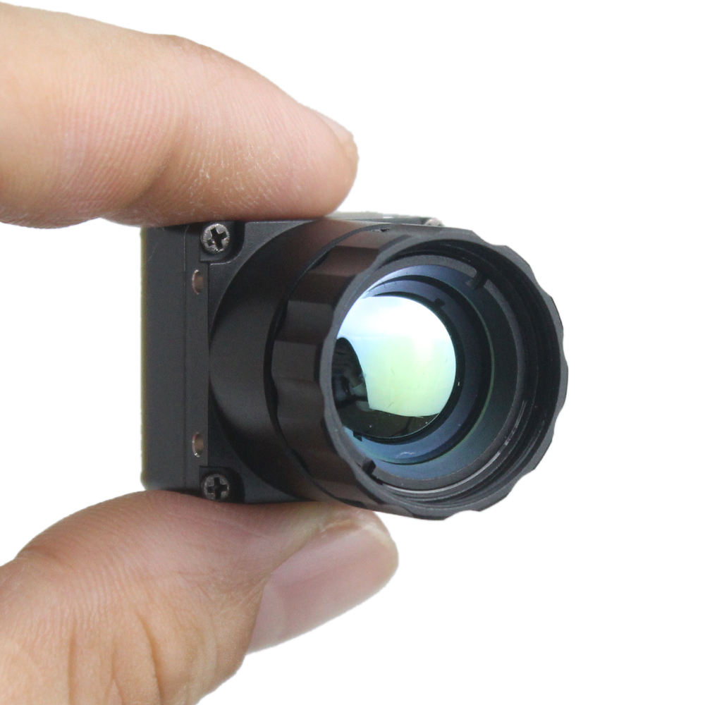
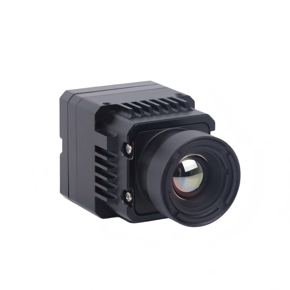
Uncooled LWIR USB Mini 640*512 Thermal Imaging Camera Core Module For Drones Similar To DJI
Designed as a versatile drop-in thermal solution, the Mini 640 core features a 21mm × 21mm cross-sectional envelope. Engineered to meet demanding requirements similar to commercial enterprise drone platforms, it supports multiple optical focal lengths—from 5mm ultra-wide lenses to 150mm telephoto optics. This optical versatility makes it suitable for short-range obstacle avoidance, mid-range industrial inspection, and long-range border security surveillance.
- ✅ Compact Footprint: 21mm × 21mm housing allows easy mechanical integration into multi-axis gimbal pods.
- ✅ Extensive Lens Range: Supports 5, 9, 13, 18, 35, 50, 75, 100, and 150 mm focal lengths.
- ✅ Resolution Output: 640×512 resolution with an optional 640×480 legacy video format.
- ✅ Environmental Stability: Built to withstand wide operational temperature ranges and high-vibration airborne environments.
| Mechanical Dimensions | Mini-Size 21 mm × 21 mm |
| Resolution Matrices | 640×512 (640×480 optional) |
| Available Optics (Focal Lengths) | 5 mm, 9 mm, 13 mm, 18 mm, 35 mm, 50 mm, 75 mm, 100 mm, 150 mm |
| Interface Support | USB / Digital Video Port / Embedded Interface Configurations |
| Application Profile | Enterprise-grade drone payloads, multi-range security systems, perimeter monitoring |
Architectural Comparison: Native MIPI vs. Multi-Interface Modularity
When selecting between these two modular thermal engines, engineering teams must evaluate their system's mechanical envelope and interface architecture:
| Architectural Metric | Mini2 MIPI Thermal Core | Mini 640 Uncooled LWIR Core |
|---|---|---|
| Primary System Interface | Native MIPI CSI-2 (Direct-to-SoC via FPC) | USB / Parallel DVP / Custom Expansion |
| Processor Data Path | Direct hardware DMA to GPU/NPU memory space | Host USB controller driver or video capture bridge |
| System Transport Latency | Sub-frame (< 2 ms) | Standard (15 ms to 35 ms) |
| Optical Flexibility | Fixed 9 mm optimized lens for wide HFOV | Wide optical portfolio: 5 mm wide up to 150 mm telephoto |
| Target Integration Envelope | Micro-gimbals, autonomous edge drones, AI trackers | DJI-type payloads, dual-spectrum pan-tilt pods |
The Mini2 640×512 MIPI Module is ideal for integrated systems running on modern SoCs like the Jetson Orin or RK3588, where minimizing weight, hardware latency, and computational overhead is paramount. Conversely, the Mini 640 Core offers modularity for long-range observation, perimeter pan-tilt-zoom (PTZ) arrays, and payload platforms requiring flexible optics up to 150 mm.
6. Deep-Dive Engineering FAQ
Why choose a native MIPI thermal imaging core over standard USB or SPI modules for Raspberry Pi/Jetson projects?
What are the main challenges when interfacing a 640x512 MIPI thermal core with an FPGA or custom carrier board?
Can these MIPI thermal cores fit into compact drone gimbals without exceeding SWaP limits?
📚 References & Further Reading
- Industry Standard: UAV airframe and stabilization integration solutions by OBSETECH
- Industry Standard: Embedded semiconductors and high-speed vision distribution by JM Chip
- Related Guide: Choosing the Right LWIR Thermal Camera Module: An OEM Guide to Edge Systems
- Related Guide: Неохлаждаемый инфракрасный модуль MIPI 640/384 9мм
- Related Guide: 1280x1024 Тепловой модуль нового поколения