
Buy Thermal Camera Core: High-Performance 640 & 384 LWIR Modules Guide
2026年9月11日
MIPI Thermal Imaging Core: High-Res Embedded Vision for Drones & Edge AI
2026年9月16日
MIPI Thermal Camera Module: Low-Latency LWIR Integration for Drones & Edge AI
In embedded vision engineering, integrating Long-Wave Infrared (LWIR) sensing into compact, autonomous edge architectures presents significant system-level challenges. Conventional thermal cores bound to USB 3.0 (UVC) or Serial Peripheral Interface (SPI) protocols frequently introduce host-side CPU overhead, unmanageable kernel buffering latencies, non-deterministic packet jitter, and severe transmission bandwidth bottlenecks. For SWaP-constrained (Size, Weight, Power, and Cost) edge platforms—such as micro-unmanned aerial vehicles (UAVs), tactical micro-gimbals, autonomous mobile robots (AMRs), and edge AI vision gateways—these protocol bottlenecks degrade real-time computer vision performance, compromise gimbal PID stabilization loops, and elevate end-to-end processing latency beyond deterministic thresholds.
The industry-standard architectural solution is the direct integration of a native mipi thermal camera module via the MIPI CSI-2 (Camera Serial Interface 2) transport layer. By interfacing uncooled microbolometer sensor readouts directly to an application processor’s native Image Signal Processor (ISP) and hardware Direct Memory Access (DMA) engine, system architects bypass operating system protocol translation layers entirely. This architectural shift enables deterministic, sub-millisecond transmission of uncompressed 14-bit or 16-bit raw radiometric data at high frame rates (30Hz to 60Hz) directly into GPU- and NPU-accessible unified memory spaces, unlocking real-time Edge AI inferencing, multi-spectral sensor fusion, target tracking, and automated industrial thermography.
Table of Contents
- 👉 1. The Physics and Protocol Architecture of MIPI CSI-2 in LWIR Imaging
- 👉 2. Embedded Software Stack: V4L2 Driver Architecture, Device Tree & Zero-Copy Pipelines
- 👉 3. Radiometric Data Processing & Edge AI Hardware Acceleration
- 👉 4. Hardware Engineering, SWaP-C Optimization & Electro-Optical Design
- 👉 5. Industrial MIPI Thermal Modules Technical Showcase & Specification Matrix
- 👉 6. Step-by-Step Integration & Troubleshooting Playbook
- 👉 7. Deep-Dive Industrial Integration FAQ
1. The Physics and Protocol Architecture of MIPI CSI-2 in LWIR Imaging
Thermal imaging sensors operate fundamentally differently from standard visible-spectrum CMOS sensors. Uncooled LWIR detectors utilize microbolometer focal plane arrays (FPAs)—typically fabricated from Vanadium Oxide (VOx) or Amorphous Silicon (α-Si)—sensitive to electromagnetic radiation within the 8 μm to 14 μm atmospheric transmission window. Each microbolometer pixel consists of an infrared absorber suspended over a silicon substrate via microscopic thermal isolation legs. When exposed to incident thermal radiation, the absorber's temperature shifts, causing a measurable change in its electrical resistance. This analog resistance variance is digitized by integrated Readout Integrated Circuits (ROICs) into high-dynamic-range raw values, typically 14-bit or 16-bit digital numbers per pixel.
Transferring these raw microbolometer data streams to an embedded host processor requires an interface that preserves signal integrity without introducing computational latencies. The MIPI Camera Serial Interface 2 (MIPI CSI-2), coupled with the physical layer (D-PHY), fulfills these requirements for embedded vision systems by transmitting serialized pixel data over point-to-point differential lanes governed by rigid hardware clocking.
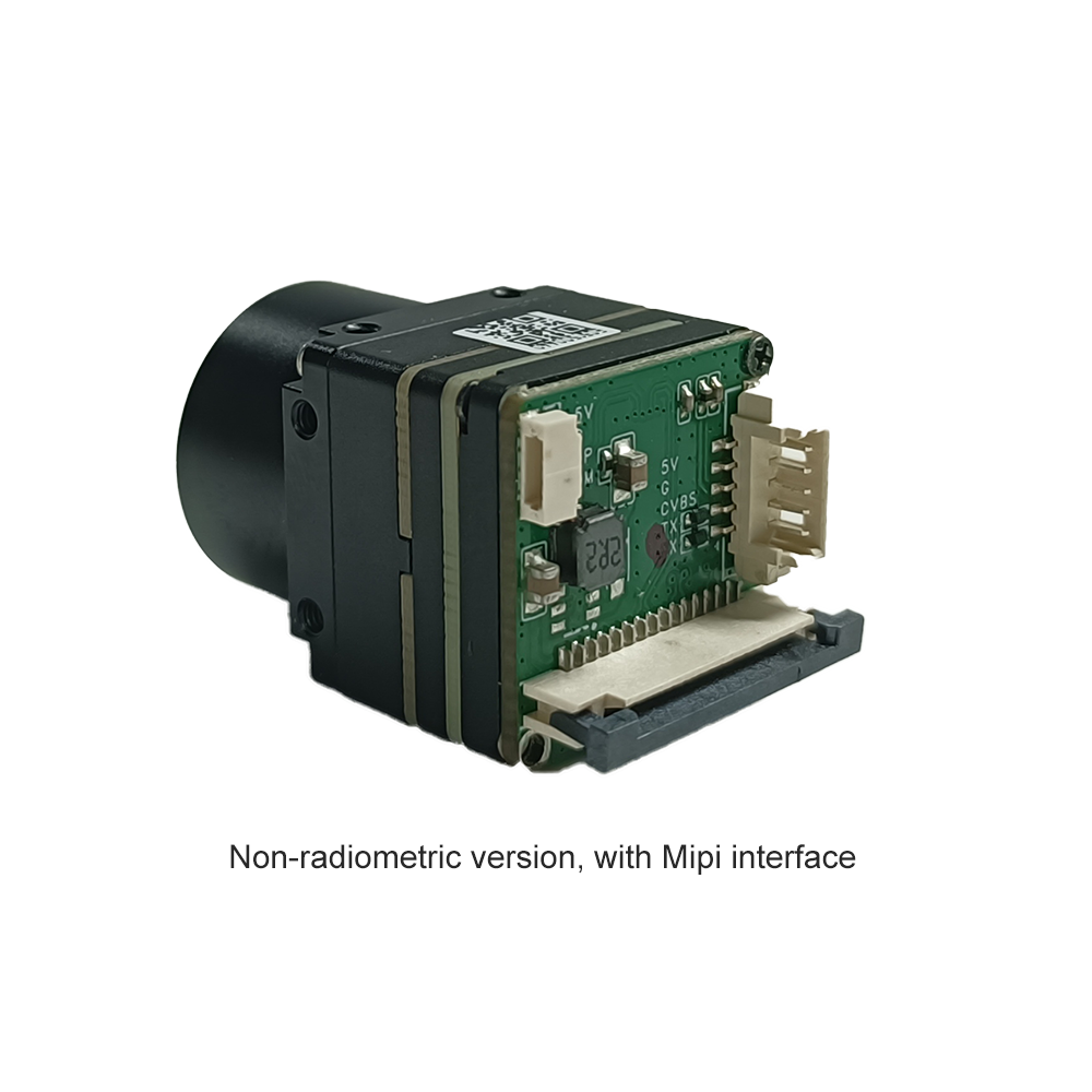
MIPI D-PHY Physical Layer Signaling Dynamics
The electrical physical layer of a modern MIPI thermal module relies on the MIPI Alliance D-PHY specification, an asynchronous source-synchronous interface featuring one differential clock lane and one, two, or four differential data lanes. The physical layer switches dynamically between two operational signaling modes:
- ⚙️ High-Speed (HS) Mode: Operates using low-voltage differential signaling (LVDS-like), with a nominal differential swing of 200 mV centered around a 200 mV common-mode voltage (VCM). In HS mode, data is serialized and transferred at throughputs ranging from 80 Mbps up to 2.5 Gbps per lane, enabling high aggregate throughput with exceptionally low radiated electromagnetic emissions.
- ⚙️ Low-Power (LP) Mode: Operates using single-ended 1.2 V CMOS signaling logic. LP mode manages line control protocols, handling frame synchronization handshakes (such as Start of Transmission [SoT] and End of Transmission [EoT]), low-power state transitions, and sleep modes (LP-11).
In contrast to visible-spectrum 4K RGB sensors that demand multi-gigabit throughput (e.g., 4K at 60 fps consuming four lanes running at greater than 1.5 Gbps per lane), an uncooled LWIR sensor operating at a resolution of 640 × 512 with a 16-bit radiometric output at 50 Hz produces an aggregate raw data payload calculated as:
Throughput = 640 × 512 × 16 bits/pixel × 50 frames/s ≈ 262.14 Mbps
This throughput requirement is comfortably managed over a single-lane (1-lane) or dual-lane (2-lane) MIPI D-PHY running at a conservative clock rate of 400 Mbps to 800 Mbps per lane. Operating at lower clock frequencies while using native differential D-PHY signaling minimizes high-frequency electromagnetic interference (EMI) across co-located RF receivers, a critical advantage when integrating sensitive communications and GNSS receivers into compact UAV platforms.
CSI-2 Packetization Protocol and Radiometric Data Types
At the CSI-2 Protocol Layer, image data is transmitted in structured packets consisting of a 4-byte Packet Header (PH), an arbitrary-length payload data sequence, and a 2-byte Packet Footer (PF) carrying a 16-bit Cyclic Redundancy Check (CRC). The Packet Header contains an 8-bit Data Identifier (DI) byte, composed of a 2-bit Virtual Channel Identifier (VC) and a 6-bit Data Type (DT) code.
Thermal modules utilize specific Data Types within the CSI-2 stream to carry raw bolometric and radiometric measurements:
- ⚙️ RAW14 (Data Type 0x2D): 14-bit uncompressed data. Microbolometers natively produce 14 bits of dynamic range. Packets are formatted by packing four 14-bit pixel values into seven consecutive 8-bit bytes, maximizing payload transmission efficiency across the physical link.
- ⚙️ RAW16 (Data Type 0x2E): 16-bit uncompressed data. Each pixel maps directly to an unsigned two-byte integer representing either linear detector response or absolute radiometric temperature values in centikelvin. RAW16 simplifies byte-alignment and memory addressing on host microprocessors.
- ⚙️ User-Defined / Embedded 8-Bit Data (Data Types 0x30 to 0x37 or 0x12): Industrial thermal modules prepend or append an "embedded line" containing operational metadata: sensor die temperature, internal shutter state, FPA housing thermistor voltage, calibration flags, and optical ambient readouts necessary for absolute radiometry calculations.
Architectural Comparison: MIPI CSI-2 vs. Alternative Embedded Interfaces
| Interface Standard | Physical Layer | Max Sustained Throughput | Glass-to-Memory Latency | Host CPU Overhead | Connector Footprint |
|---|---|---|---|---|---|
| MIPI CSI-2 | Differential D-PHY (HS/LP) | Up to 2.5 Gbps per lane | < 1.5 ms (Direct DMA) | < 2% (Hardware ISP/DMA) | Ultra-compact micro-coaxial or 0.5mm FPC |
| USB 3.0 / UVC | Differential SuperSpeed | ~3.2 Gbps (Packet-bound) | 15 to 45 ms (Variable Jitter) | 12% to 25% (Kernel polling & copies) | Bulky USB Type-C or Type-A receptacles |
| SPI (Quad/Octal) | Single-Ended Synchronous | ~50 to 100 Mbps | 40 to 120 ms (Buffer limited) | 30% to 60% (High Interrupt Load) | Standard board-to-board pin headers |
| Parallel (DVP) | 8/14-bit Single-Ended CMOS | ~600 Mbps | 3 to 8 ms | 5% to 10% | Wide 30+ pin ribbon (High EMI profile) |
2. Embedded Software Stack: V4L2 Driver Architecture, Device Tree & Zero-Copy Pipelines
Direct integration of a mipi thermal camera module into modern Linux host SoCs—such as NVIDIA Jetson Orin/Xavier, Rockchip RK3588, NXP i.MX8M, or Raspberry Pi Compute Module 4/5—requires configuring the underlying kernel driver stack. Thermal cores are registered within the Linux Video4Linux2 (V4L2) framework as camera sub-devices managed through the Media Controller API.
The host system architecture follows a layered driver model: the SoC's hardware CSI-2 receiver endpoint captures incoming differential serial packets, passes them to an internal DMA channel, and transfers data into physical memory buffers. The kernel driver sets up streaming parameters via an I2C or UART control interface, ensuring synchronized exposure, framing, and on-chip thermal processing states.
The Device Tree Source (DTS) Architecture
The Linux Device Tree defines the hardware topology, linking the SoC's CSI-2 receiver endpoint to the thermal module's output port, specifying pin configurations for clock generation, reset lines, and the Camera Control Interface (typically an I2C bus operating in Fast-mode at 400 kHz).
Below is a baseline DTS node implementation for a system running a dual-lane MIPI thermal core connected to an embedded SoC:
// Device Tree Source (DTS) snippet for Industrial MIPI Thermal Module
&i2c1 {
    status = "okay";
    clock-frequency = <400000>;
    #address-cells = <1>;
    #size-cells = <0>;

    thermal_mipi: camera@38 {
        compatible = "purpleriver,mini2-mipi-thermal";
        reg = <0x38>;

        /* Hardware Reset and Power Control Lines */
        reset-gpios = <&gpio1 14 GPIO_ACTIVE_LOW>;
        powerdown-gpios = <&gpio1 15 GPIO_ACTIVE_HIGH>;
        clocks = <&cru CLK_CAM_EXT>;
        clock-names = "xvclk";
        assigned-clocks = <&cru CLK_CAM_EXT>;
        assigned-clock-rates = <24000000>;

        /* V4L2 Media Bus Port Definition */
        port {
            thermal_to_csi: endpoint {
                remote-endpoint = <&csi_in_thermal>;
                data-lanes = <1 2>;
                clock-lanes = <0>;
                clock-noncontinuous;
                link-frequencies = /bits/ 64 <200000000 400000000>;
            };
        };
    };
};

&csi2_host {
    status = "okay";
    ports {
        #address-cells = <1>;
        #size-cells = <0>;
        port@0 {
            reg = <0>;
            csi_in_thermal: endpoint {
                remote-endpoint = <&thermal_to_csi>;
                data-lanes = <1 2>;
            };
        };
    };
};
For embedded system developers working through hybrid visual-thermal builds, evaluating specialized hardware integration workflows is critical. Learn more about sensor topology alignments and dual-band configurations in our CMOS sensor thermal camera module integration guide.
V4L2 Sub-Device Driver Core Implementation
The kernel driver implements standard V4L2 sub-device operations structures: v4l2_subdev_core_ops, v4l2_subdev_video_ops, and v4l2_subdev_pad_ops. When user-space applications initiate video capture via the VIDIOC_STREAMON ioctl, the driver configures the internal FPGA or ASIC of the thermal core over I2C, places the microbolometer sensor into continuous readout mode, and primes the host-side CSI-2 receiver.
static const struct v4l2_subdev_video_ops thermal_video_ops = {
    .s_stream = purpleriver_thermal_s_stream,
    .g_frame_interval = purpleriver_thermal_g_frame_interval,
    .s_frame_interval = purpleriver_thermal_s_frame_interval,
};

static const struct v4l2_subdev_pad_ops thermal_pad_ops = {
    .enum_mbus_code = purpleriver_thermal_enum_mbus_code,
    .get_fmt        = purpleriver_thermal_get_fmt,
    .set_fmt        = purpleriver_thermal_set_fmt,
};

static int purpleriver_thermal_s_stream(struct v4l2_subdev *sd, int enable)
{
    struct purpleriver_dev *sensor = to_purpleriver_dev(sd);
    int ret = 0;

    mutex_lock(&sensor->lock);
    if (enable) {
        /* Initialize core registers: Set 14-bit radiometric readout, enable streaming */
        ret = purpleriver_write_reg(sensor->client, REG_SENSOR_MODE, MODE_STREAMING_RAW14);
        if (ret < 0) goto exit;
        ret = purpleriver_write_reg(sensor->client, REG_STREAM_ENABLE, 0x01);
    } else {
        ret = purpleriver_write_reg(sensor->client, REG_STREAM_ENABLE, 0x00);
    }
exit:
    mutex_unlock(&sensor->lock);
    return ret;
}
Zero-Copy Memory Management via DMABUF Architecture
High-throughput radiometric image processing cannot afford CPU-driven memory copies (memcpy) across user-kernel boundaries. Transferring 640 × 512 16-bit frames at 50 Hz using conventional read operations introduces memory bus saturation and increases frame delivery latency by 15 ms to 30 ms.
To achieve sub-millisecond transfer latencies, modern edge pipelines utilize DMABUF memory sharing:
- ⚙️ Buffer Allocation: Contiguous memory blocks are pre-allocated in system RAM via the Linux Contiguous Memory Allocator (CMA) or hardware buffer allocators (such as NVIDIA
NvBufSurfaceor Rockchip MPP/RGA memory pools). - ⚙️ Descriptor Export: These allocated buffers are exported to user-space applications as native Linux file descriptors (DMABUF FDs).
- ⚙️ Hardware DMA Streaming: The host SoC's MIPI CSI-2 hardware interface transfers incoming packet payloads directly into these physical memory addresses without host CPU intervention.
- ✅ Direct NPU/GPU Ingestion: Edge AI inference engines (such as TensorRT, DeepStream, or ONNX Runtime) bind directly to these shared memory pointers. Zero-copy access eliminates memory copying overhead and achieves glass-to-inference execution latencies below 1.5 milliseconds.
3. Radiometric Data Processing & Edge AI Hardware Acceleration
Unlike visible-spectrum image sensors that output ready-to-display sRGB color spaces, uncooled LWIR sensors capture raw thermal flux emitted across the scene. The digitized output corresponds to detector resistance rather than human visual perceptions. Developing real-time vision pipelines requires applying specialized calibrations and transformations to extract accurate temperature information.
Non-Uniformity Correction (NUC) and Bad Pixel Replacement (BPR)
Microbolometer focal plane arrays exhibit pixel-to-pixel variations in responsivity and dark offset voltage due to semiconductor fabrication tolerances. The response of an individual pixel i is represented mathematically by the linear model:
Vi(T) = Gi × Φ(T) + Oi
Where:
- ⚙️ Gi: Individual pixel responsivity (gain) coefficient.
- ⚙️ Φ(T): Incident infrared irradiance originating from target scene temperature T.
- ⚙️ Oi: Individual spatial offset, heavily influenced by the focal plane array's internal substrate temperature.
To eliminate fixed-pattern noise (FPN) and achieve thermal sensitivities below 40 mK, the thermal processing engine performs three distinct operations:
- ⚙️ Two-Point Gain Calibration: Calibrates individual pixel gain coefficients (Gi) using uniform blackbody calibration sources across two known reference temperatures (T1 and T2). These coefficients are stored in non-volatile sensor memory.
- ⚙️ Offset Compensation (Shutter Calibration): An electromechanical shutter periodically moves into the optical path for 100 to 300 ms, exposing the array to a uniform thermal reference. The module recalculates offset tables (Oi) to compensate for ambient thermal drift. High-end cores deploy shutterless algorithms that continuously update offset matrices using real-time temperature readings from internal housing and lens thermistors.
- ⚙️ Bad Pixel Replacement (BPR): Dead, unresponsive, or noisy pixels that fall outside three standard deviations of the array's median Gaussian distribution are flagged during factory calibration. In operation, hardware pipelines replace these values in real time using 3×3 median or bilinear interpolation from surrounding functional pixels.
Conversion from Raw Digital Values to Absolute Temperature
Following Non-Uniformity Correction, the module produces a 14-bit or 16-bit linear digital output (Digital Numbers, or DN). Converting these values into absolute radiometric temperature units (Kelvin or Celsius) requires calculating the inverted Planck radiation function:
Ttarget = B / ln( R1 / (R2 × (DN - Odrift)) + F )
Where R1, R2, B, and F represent empirical calibration constants established via laboratory blackbody profiling, and Odrift accounts for real-time substrate temperature variations. In industrial radiometric modules, this calculation is executed either on the internal module processor or mapped into optimized vector execution units (such as ARM NEON or NVIDIA CUDA kernels) on the host processor.
High-Contrast Dynamic Range Compression for Neural Networks
Contemporary Edge AI object detection models (such as YOLOv8, YOLOv10, or RT-DETR) are architected for 3-channel 8-bit input tensors (values ranging from 0 to 255). Linearly downscaling an uncompressed 14-bit radiometric dynamic range (0 to 16,383) to 8-bit discards fine thermal gradients, often obscuring faint targets (such as humans or distant vehicles) against warm backgrounds.
To preserve target details, the software pipeline splits the incoming MIPI CSI-2 stream into dual processing branches:
- ⚙️ The Radiometric Analytic Stream: Preserves the raw 14-bit or 16-bit linear radiometric depth. This pipeline feeds threshold algorithms, spot temperature queries, and automated fire or overheating alarm routines.
- ⚙️ The Vision AI Inference Stream: Passes raw data through a Digital Detail Enhancement (DDE) filter and Contrast Limited Adaptive Histogram Equalization (CLAHE). These algorithms separate the scene into a low-frequency base layer (representing overall background temperature gradients) and a high-frequency detail layer (highlighting sharp boundaries, edges, and signatures). The layers are dynamically balanced into an 8-bit contrast-enhanced representation, maximizing edge feature extraction for neural network inference.
For additional details on deploying deep learning models over localized radiometric stream architectures, review our technical guide on промышленные мини-модули LWIR с ИИ (industrial mini-LWIR modules with AI).
4. Hardware Engineering, SWaP-C Optimization & Electro-Optical Design
Deploying thermal vision payloads into airborne micro-gimbals, handheld inspection equipment, and small mobile robots demands strict attention to Size, Weight, Power, and Cost (SWaP-C) budgets alongside high-speed printed circuit board (PCB) design standards.
High-Speed PCB Layout & Signal Integrity Guidelines
The MIPI D-PHY physical layer operates with rapid signal rise and fall times (tr, tf < 200 ps). High-speed layout oversights can cause transmission line reflections, differential impedance mismatches, and severe packet corruption:
- ⚙️ Differential Impedance Control: All differential clock and data trace pairs must be routed to maintain a tightly controlled 100 Ω ± 10% differential impedance (50 Ω single-ended reference).
- ⚙️ Intra-Pair Skew Matching: Trace length differences between positive (P) and negative (N) conductors within a differential pair must not exceed 0.15 mm (< 1 ps phase skew). Excessive intra-pair skew degrades common-mode rejection and increases electromagnetic emissions.
- ⚙️ Inter-Pair Skew Matching: Length mismatches between the clock lane pair and any corresponding data lane pair must remain below 0.5 mm to ensure timing margins are preserved across the high-speed receiver.
- ⚙️ Continuous Reference Plane: MIPI traces must be routed across unbroken, continuous ground reference planes. Traces must not cross splits, power planes, or voids, which create impedance discontinuities and generate common-mode noise.
- ⚙️ Interconnect Selection: Gimbal payloads require specialized low-profile micro-coaxial ribbons or shielded flexible printed circuits (FPC). High-reliability connectors from precision manufacturers like Amphenol maintain signal integrity across moving gimbal pivots and slip rings without introducing mechanical binding.
Optical Materials Engineering: Germanium vs. Chalcogenide Glass
Because optical glass is opaque in the 8 μm to 14 μm infrared band, uncooled LWIR lenses require specialized optical substrates:
- ⚙️ Monocrystalline Germanium (Ge): Germanium exhibits a high refractive index (n ≈ 4.00 at 10 μm), enabling compact, low-aberration multi-element optical assemblies. However, Germanium features a high temperature-dependent refractive index coefficient (dn/dt = 3.96 × 10⁻⁴/°C) and exhibits optical absorption runaway above +100°C. It is also dense and represents a significant material cost.
- ✅ Chalcogenide Glass: Engineered chalcogenide glasses—such as those produced by LightPath Technologies—offer lower mass, reduced material costs, and significantly lower dn/dt values. These characteristics enable passive athermalization across wide temperature ranges (-40°C to +85°C) without motorized focus mechanics, reducing gimbal payload mass.
Engineers designing defense or long-range intelligence, surveillance, and reconnaissance (ISR) payloads can contrast these lightweight short-to-medium-range micro-optics against larger systems in our breakdown of the 1280x1024 12μm long range thermal imaging sight scope.
5. Industrial MIPI Thermal Modules Technical Showcase & Specification Matrix
Below is a detailed examination of two industrial-grade MIPI thermal camera modules optimized for unmanned payloads, tactical micro-gimbals, and embedded edge computing architectures.
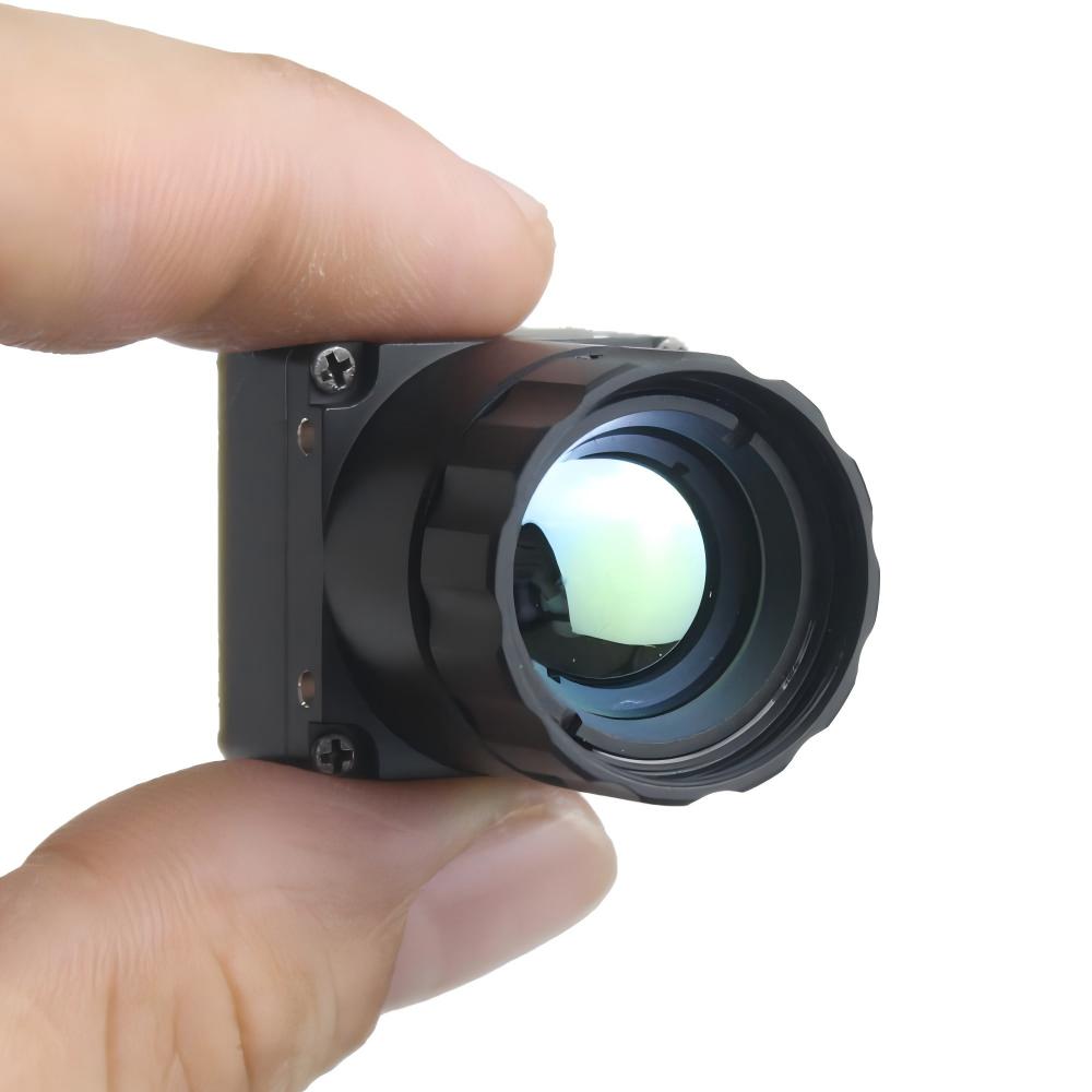
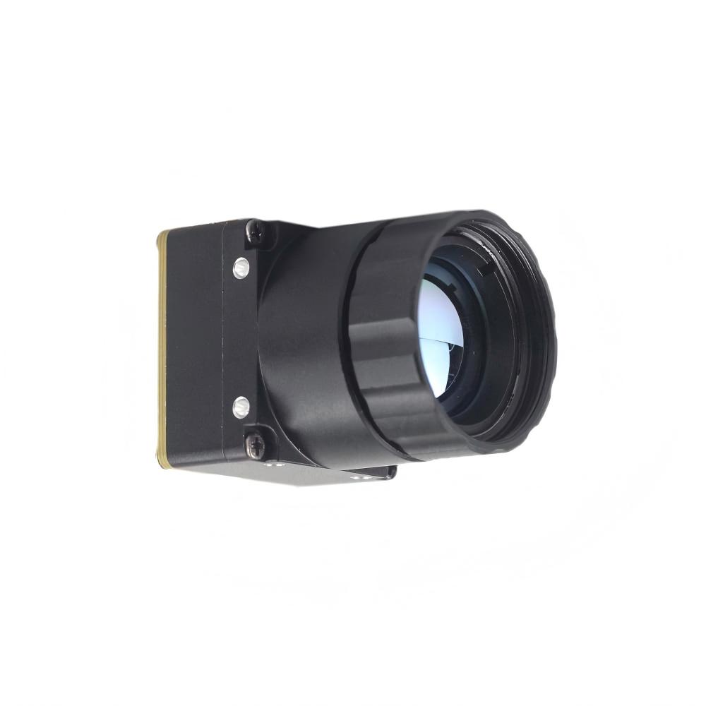
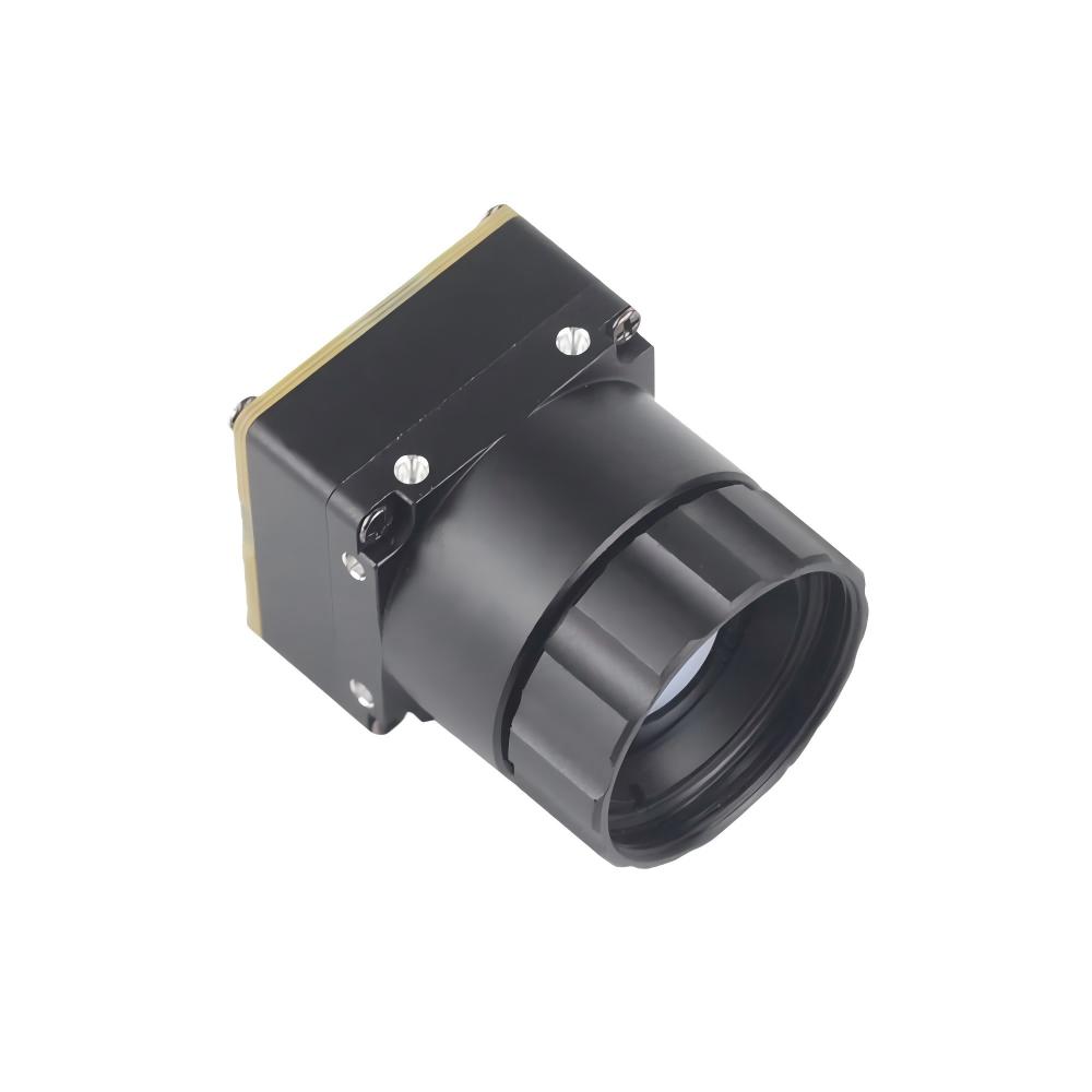
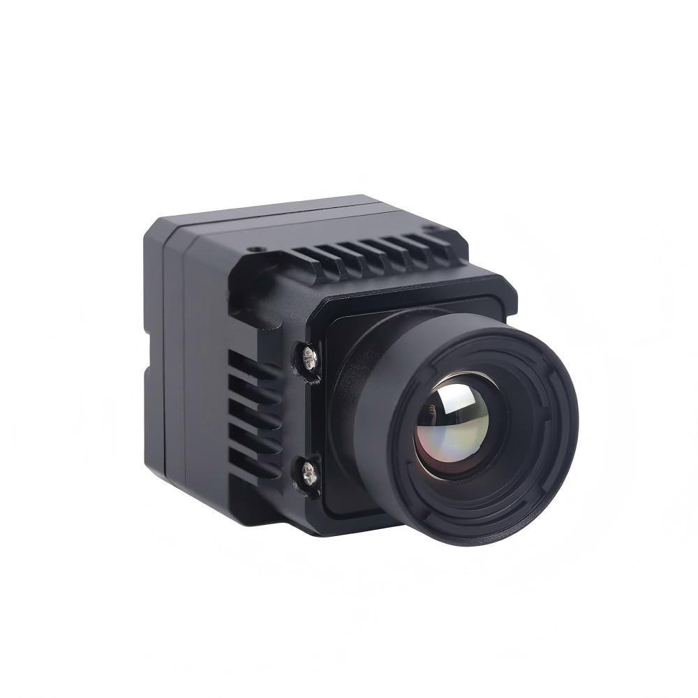
Purpleriver Mini2 640x512 9mm Uncooled MIPI Thermal Imaging Module
The Mini2 640x512 9mm is an uncooled LWIR camera module designed for airborne drone payloads, tactical gimbals, and real-time robotic vision systems. Delivering sharp and crisp image presentation, compact form factor, and low unit cost, this module integrates an uncooled VOx detector with a 12 μm pixel pitch and an athermalized 9mm lens. It supports native MIPI CSI-2 digital output for direct integration into embedded host processors, bypassing intermediate interface bridges.
- ⚙️ Resolution: 640 × 512 Active Pixels (VGA Thermal)
- ⚙️ Pixel Pitch: 12 μm Vanadium Oxide (VOx) Microbolometer
- ✅ Thermal Sensitivity: ≤ 40 mK (NETD at f/1.0, 300K)
- ⚙️ Video Output: 2-lane MIPI CSI-2, DVP, or USB options
- ✅ Power Consumption: < 900 mW (Steady State)
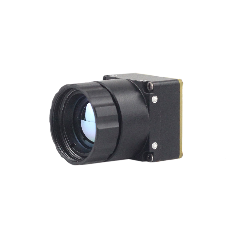
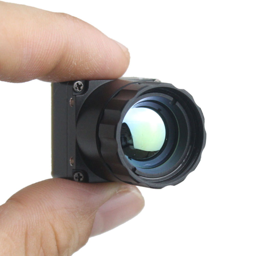
Purpleriver Mini 256x192 Uncooled LWIR Thermal Camera Module
The Mini 256 Uncooled LWIR thermal Camera Module adopts high-performance infrared detectors designed for clear thermal imaging and accurate temperature measurement. Engineered to capture infrared radiation and output uniform thermal imagery with integrated radiometry, its ultra-lightweight profile suits weight-critical deployments, including mine detection drones, search and rescue robots, and micro-UAV swarms.
- ⚙️ Resolution: 256 × 192 Active Pixels
- ⚙️ Pixel Pitch: 12 μm High-Sensitivity Uncooled Microbolometer
- ✅ Thermal Sensitivity: ≤ 50 mK (NETD at f/1.0)
- ⚙️ Precision Radiometry: Point, line, and area temperature tracking with accurate output
- ✅ Weight Profile: ≤ 12 g total mass (SWaP-optimized)
Comprehensive Specification Matrix
| Specification Parameter | Purpleriver Mini2 640x512 9mm | Purpleriver Mini 256x192 Core |
|---|---|---|
| Detector Architecture | Uncooled VOx Microbolometer FPA | Uncooled LWIR Microbolometer FPA |
| Array Resolution | 640 × 512 pixels | 256 × 192 pixels |
| Pixel Pitch | 12 μm | 12 μm |
| Spectral Sensitivity | 8 μm to 14 μm (LWIR) | 8 μm to 14 μm (LWIR) |
| NETD Sensitivity | ≤ 40 mK (f/1.0 at 300K) | ≤ 50 mK (f/1.0 at 300K) |
| Frame Output Rates | 25 Hz / 30 Hz / 50 Hz | 25 Hz / 30 Hz |
| Digital Interfaces | MIPI CSI-2 (2-lane) / DVP / USB | MIPI CSI-2 (1 or 2-lane) / SPI |
| Control Command Bus | I2C / UART (Up to 921,600 bps) | I2C / UART |
| Radiometric Range | -20°C to +150°C (High Gain); up to +550°C (Low Gain) | -20°C to +150°C (Industrial Radiometry) |
| Measurement Accuracy | ±2°C or ±2% of reading | ±2°C or ±2% of reading |
| Standard Optic | 9mm (HFOV ≈ 48°) Athermalized | Integrated Wide-Angle Micro-Lens |
| Operational Power | < 900 mW (Continuous operation) | < 450 mW (Ultra-low power) |
| Module Mass | ≈ 18 g (Core) / 28 g (With 9mm Lens) | ≤ 12 g Total |
6. Step-by-Step Integration & Troubleshooting Playbook
Executing a reliable integration of a MIPI thermal camera module into an embedded carrier board requires following a structured hardware and software validation methodology.
Step 1: Hardware Rail Verification
Prior to powering the module, verify all voltage supply rails using an oscilloscope. Uncooled microbolometers are sensitive to power supply noise. Ensure the analog supply rail (VDD_ANA) exhibits less than 10 mVRMS ripple. High power ripple directly degrades the sensor's Noise Equivalent Temperature Difference (NETD), introducing horizontal banding across the raw image stream.
Step 2: Device Tree Compilation and Kernel Registration
Compile the Device Tree source overlay and load the driver kernel module into the Linux kernel space. Verify that the thermal sub-device acknowledges I2C commands using standard Linux utilities:
# Verify module acknowledges on I2C bus 1 at address 0x38
i2cdetect -y -r 1

# Inspect the kernel ring buffer for successful sub-device probing
dmesg | grep -i purpleriver
# Expected Output:
# [    4.120349] purpleriver_thermal 1-0038: Sensor probed successfully. Model: Mini2-640
# [    4.121110] purpleriver_thermal 1-0038: Subdev registered as /dev/v4l-subdev2
Step 3: Stream Capture Verification with V4L2 Utilities
Query the host video device node using v4l2-ctl to confirm supported pixel formats and negotiate the streaming format before launching higher-level vision applications:
# Query available pixel formats on host video node
v4l2-ctl --device=/dev/video0 --list-formats-ext

# Capture 100 test frames directly to file using direct MMAP DMA
v4l2-ctl --device=/dev/video0 \
         --set-fmt-video=width=640,height=512,pixelformat='Y16 ' \
         --stream-mmap --stream-count=100 \
         --stream-to=test_stream.raw
Step 4: Hardware-Accelerated GStreamer Pipeline Integration
To feed raw radiometric frames directly into hardware-accelerated processing pipelines, configure a zero-copy GStreamer pipeline. The pipeline below splits the incoming 16-bit raw data, directing one stream to hardware color-mapping for operator display and the other directly to an appsink for neural network inference:
gst-launch-1.0 v4l2src device=/dev/video0 ! \
    video/x-raw, format=GRAY16_LE, width=640, height=512, framerate=30/1 ! \
    tee name=thermal_tee \
    thermal_tee. ! queue leaky=1 ! \
        nvvideoconvert ! \
        video/x-raw(memory:NVMM), format=RGBA ! \
        nvdsosd ! nveglglessink sync=false \
    thermal_tee. ! queue leaky=1 ! \
        appsink name=radiometric_sink emit-signals=true max-buffers=1 drop=true
Diagnostic Matrix: Common Integration Pitfalls
| Reported Fault | Root Cause Analysis | Engineering Resolution |
|---|---|---|
| "MIPI CSI-2 FIFO Overflow / Packet CRC Error" | Differential length mismatch or clock-lane skew exceeding physical receiver margins. | Check trace routing; enforce intra-pair skew < 0.15mm. Ensure continuous ground plane under high-speed traces. |
| Driver fails to initialize: "LP-11 State Timeout" | Host receiver timed out waiting for module D-PHY to enter Low-Power standby state before High-Speed transmission. | Add a hardware reset hold time (trst > 15 ms) in DTS. Match clock mode (continuous vs. non-continuous) with module settings. |
| Frame displays severe fixed pattern noise (FPN) | Internal microbolometer temperature shifted during continuous operation without offset recalibration. | Trigger an internal shutter calibration via I2C command, or enable continuous shutterless compensation in the module's driver controls. |
Mini 640×512 Thermal Imaging Core Demo Video
7. Deep-Dive Industrial Integration FAQ
Why choose a MIPI CSI-2 thermal camera module over USB or SPI interfaces for embedded vision?
SPI interfaces present bandwidth constraints. Standard single or quad SPI buses max out between 50 Mbps and 100 Mbps, making them incapable of transporting an uncompressed 640 × 512 14-bit stream at 30 Hz to 50 Hz without aggressive down-sampling or frame drops. In contrast, MIPI CSI-2 interfaces directly with the host processor's camera subsystem. Uncompressed raw radiometric data is delivered via hardware Direct Memory Access (DMA) into unified memory buffers with less than 2% CPU overhead and under 1.5 ms of glass-to-memory latency. This deterministic transfer is essential for mission-critical Edge AI target tracking and multi-sensor fusion.
How complex is embedded Linux driver bring-up for Purpleriver MIPI thermal modules?
The kernel driver registers as a standard v4l2_subdev, exposing interfaces for format configuration, framerate negotiation, and thermal parameter control via standard or extended V4L2 controls. Once the driver binds to the sensor, user-space utilities like media-ctl link the camera pad to the host SoC's capture interface. Reference Board Support Packages (BSPs), Device Tree source overlays, and pre-compiled GStreamer pipelines are available for platforms including NVIDIA Jetson (JetPack 5.x/6.x), Rockchip RK3588, and Raspberry Pi CM4. These resources help engineering teams complete driver integration in a few working days rather than months.
Are these MIPI thermal modules suitable for weight-sensitive drone and gimbal applications?
Operating power consumption is maintained below 900 mW for the Mini2 and under 450 mW for the Mini 256. This low power draw extends flight endurance and minimizes internal heat buildup. In sealed IP67 payloads, excess internal heat can cause microbolometer temperature drift and force repeated shutter recalibrations; these modules' low power dissipation helps preserve thermal stability. Additionally, their fine-pitch flexible printed circuit (FPC) connections can route cleanly through compact mechanical gimbal joints and slip rings without introducing mechanical drag on stabilization motors.
📚 References & Further Reading
- ⚙️ Industry Standard: High-speed interconnect and micro-coaxial cable assemblies for aerospace and robotic vision: Amphenol Corporation
- ⚙️ Industry Standard: Molded chalcogenide infrared optical engineering and passive athermalization: LightPath Technologies
- ⚙️ Related Guide: Multi-sensor design and dual-band optical alignment: CMOS Sensor Thermal Camera Module Integration Guide
- ⚙️ Related Guide: Advanced neural network deployment over localized infrared arrays: Промышленные мини-модули LWIR с ИИ (Industrial Mini LWIR Modules with AI)
- ⚙️ Related Guide: High-definition tactical electro-optics: 1280x1024 12μm Long Range Thermal Imaging Sight Scope