
MIPI Thermal Imaging Core: High-Res Embedded Vision for Drones & Edge AI
2026年9月16日
Uncooled MIPI Thermal Camera Core: High-Res Embedded Vision Guide for Drones & Robotics
2026年9月17日
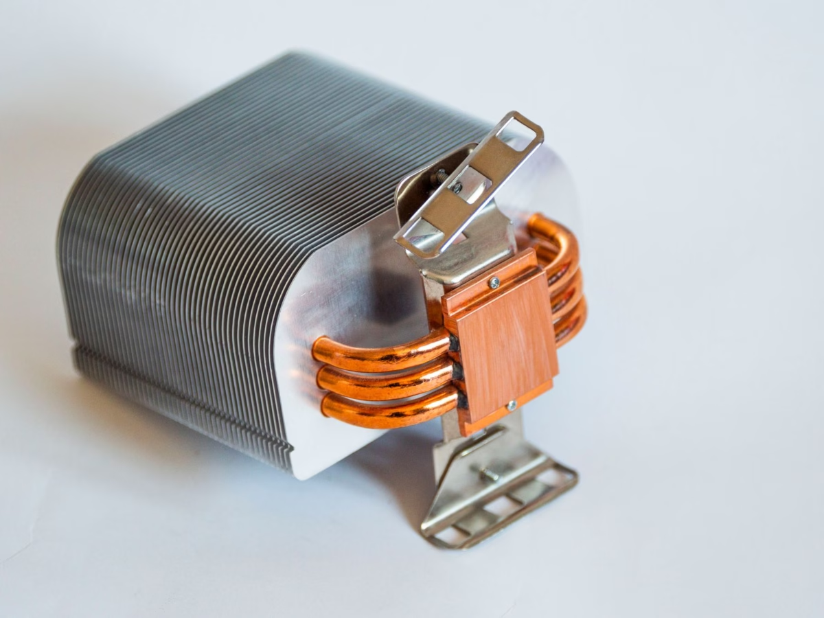
640x512 MIPI Thermal Module: High-Res OEM Camera Core for Drones & Embedded AI
In modern autonomous aerospace and intelligent edge systems, conventional optical vision falters under degraded visual environments (DVE)—including zero-illumination night ops, thick fog, dense smoke, and heavy foliage. Integrating a high-resolution uncooled long-wave infrared (LWIR) imaging core is no longer optional; it is the baseline requirement for mission-critical situational awareness and target tracking. For embedded systems engineers and payload architects, the 640x512 MIPI thermal module represents the sweet spot of spatial fidelity, thermal sensitivity, and strict Size, Weight, Power, and Cost (SWaP-C) optimization. By eliminating the protocol overhead, multi-chip bridging latencies, and host CPU bottlenecks typical of legacy USB or Ethernet streaming designs, native MIPI CSI-2 cores push unprocessed thermal sensor matrices directly into hardware ISP and GPU pipelines.
Choosing the proper microbolometer core demands an analytical evaluation of hardware interconnects, pixel pitch physics, radiometric precision, and kernel-level software driver availability. Transitioning from legacy 17µm sensors to modern 12µm wafer-level packaged (WLP) focal plane arrays allows system integrators to cut optical assembly weight by more than 40% while quadrupling resolution over legacy 384×288 baselines. This blueprint delivers a technical analysis of 640x512 uncooled thermal imaging cores, breaking down sensor physics, MIPI CSI-2 hardware interfacing, embedded Linux driver deployment, and multi-sensor payload optimization for next-generation unmanned aerial vehicles (UAVs) and edge AI platforms.
Table of Contents
- 👉 1. MIPI CSI-2 Architecture vs. Legacy Embedded Thermal Interfacing
- 👉 2. Uncooled Microbolometer Physics: The 12µm Pixel Pitch Advantage
- 👉 3. Real OEM Product Specifications: Mini2 & MD Series Core Lineup
- 👉 4. UAV SWaP-C Payload Engineering & Aerial Integration
- 👉 5. Edge AI Pipelines: Processing 640x512 Thermal Streams on Linux/RTOS
- 👉 6. Electrical, Pinout, and Mechanical Interfacing Standards
- 👉 7. Industrial Engineering Technical FAQ
1. MIPI CSI-2 Architecture vs. Legacy Embedded Thermal Interfacing
1.1 Direct Memory Access (DMA) & Zero-Copy ISP Pipelines
Traditional embedded infrared camera integrations rely heavily on USB 2.0/3.0 (UVC) or Ethernet (GigE Vision) buses. While convenient for benchtop prototyping, these consumer and industrial interfaces introduce severe packetization penalties, non-deterministic packet delays, and multiple kernel-space to user-space memory copies. In high-performance autonomous navigation, targeting, and edge intelligence, a 640x512 MIPI thermal module completely bypasses these bottlenecks by operating natively over the Mobile Industry Processor Interface Camera Serial Interface 2 (MIPI CSI-2) protocol.
In a typical USB 3.0 or GigE Vision pipeline, the raw digital counts from the microbolometer's Readout Integrated Circuit (ROIC) are digitized, passed through an intermediary micro-controller or USB interface bridge, converted into bulk transfer packets, processed by host controller interrupts, and copied across OS network/USB buffers before reaching user application space. This software-heavy sequence incurs an end-to-end latency penalty of 30 to 80 milliseconds and consumes 15% to 25% of the host CPU's compute bandwidth.

Conversely, the native MIPI CSI-2 pipeline streams uncompressed 14-bit or 16-bit raw digital thermal pixel values directly from the on-die Analog-to-Digital Converter (ADC) through an ultra-low-power MIPI D-PHY transmitter. The differential data lanes feed straight into the host processor's hardware CSI receiver. By coupling this physical connection with a direct Video4Linux2 (V4L2) driver layer using Direct Memory Access (DMA) engine primitives, memory buffers are allocated directly within unified system memory. Compute engines on platforms like the NVIDIA Jetson Orin Nano, AGX Orin, or NXP i.MX8M read the raw focal plane array (FPA) data via shared memory pointers with zero CPU overhead. This architecture cuts glass-to-memory latency down to an imperceptible 2 to 5 milliseconds, releasing vital processing cycles for real-time neural network inference and low-latency flight controls.
1.2 Latency, Protocol Overhead, and Jitter Analysis: MIPI vs. USB3 vs. GigE
For closed-loop systems such as high-speed drone navigation, agile counter-UAS platforms, and dynamic target-tracking gimbals, the temporal determinism of the video pipeline is as critical as its spatial resolution. Unbounded jitter introduced by software stacks can destabilize Kalman filters and break high-speed visual-inertial odometry (VIO) loops.
| Metric | Native MIPI CSI-2 (Purpleriver Mini2) | USB 3.0 (UVC Class) | GigE Vision (Industrial RJ45) | Digital Video Port (DVP Parallel) |
|---|---|---|---|---|
| End-to-End Latency | < 2 to 5 ms | 30 to 80 ms | 25 to 60 ms | < 5 ms |
| Latency Determinism | Hard Real-Time (< 0.2ms jitter) | Non-Deterministic (±12ms) | Semi-Deterministic (±4ms) | Hard Real-Time (< 0.2ms) |
| Host CPU Overhead | < 3% (DMA Driven) | 12% to 28% (Interrupt bound) | 8% to 18% (Network stack bound) | < 3% (Direct memory write) |
| Interconnect Footprint | Ultra-thin FPC / Micro-coax | Bulky USB-C / Micro-B | Heavy Shielded CAT6 / RJ45 | Wide Ribbon Cable (20-30 pins) |
| EMI / RF Signature | Ultra-Low (200mV Differential) | Moderate (Harmonic interference) | Low (Transformer isolated) | Severe (Full 3.3V CMOS swings) |
From an electromagnetic compatibility (EMC) perspective, parallel digital interfaces (DVP) toggle 16 to 24 single-ended traces at high frequencies with full 3.3V or 1.8V CMOS logic swings. This creates significant radio frequency interference (RFI) that can desensitize adjacent GPS, RTK, and telemetry transceivers inside crowded UAV avionics bays. MIPI CSI-2 operates on a Low-Voltage Differential Signaling (LVDS) physical layer with an ultra-small signal swing of approximately 200 mV. The tightly coupled differential trace pairs provide outstanding common-mode noise rejection and virtually eliminate parasitic EMI radiation.
1.3 D-PHY Lane Topologies for High-Framerate LWIR Streams
The physical layer (PHY) of a 640x512 uncooled thermal core uses the MIPI Alliance D-PHY specification, featuring a forward source-synchronous clock scheme. A standard deployment utilizes one differential clock lane and either one or two differential data lanes.
Calculating the raw digital bandwidth requirement demonstrates how efficiently MIPI accommodates uncompressed thermal video streams:
Total Pixels per Frame = 640 × 512 = 327,680 pixels
Bits per Pixel (Uncompressed Raw 14-bit in 16-bit Container) = 16 bits
Data per Frame = 327,680 × 16 bits = 5,242,880 bits (~5.24 Mb)
Throughput at 50 Hz Frame Rate = 5,242,880 bits × 50 fps = 262.14 Mbps
Line Protocol & Framing Overhead (~20% Horizontal/Vertical Blanking) = ~315 Mbps
A single MIPI D-PHY v1.1 lane easily supports up to 1.5 Gbps, while D-PHY v1.2 scales to 2.5 Gbps per lane. Therefore, a single differential data lane can easily carry a 16-bit 640x512 thermal stream at 50Hz or 60Hz. Configuring the core to utilize two differential data lanes allows engineers to halve the transmission clock frequency to roughly 150–200 MHz. This clock reduction enhances signal integrity across longer, articulated flexible flat circuits (FFC) routed through 3-axis brushless gimbal slip rings.
2. Uncooled Microbolometer Physics: The 12µm Pixel Pitch Advantage
2.1 Spatial Resolution, DRI Ranges, and Optical Sizing Benefits
Uncooled microbolometers function by converting incident Long-Wave Infrared radiation (8µm to 14µm) into a measurable change in electrical resistance across a thermally isolated micro-membrane. The physical pitch—the center-to-center distance between adjacent detector pixels—is the single most decisive factor dictating the optical physics, thermal sensitivity, and overall mass of an electro-optical payload.
For an equivalent optical field of view, the focal length of the objective lens scales directly in proportion to the pixel pitch:
f = (p × d) / Ht
where f is the lens focal length, p is the pixel pitch, d is target distance, and Ht is the target height projected across the detector. When transitioning from older 17µm pixel detectors to a cutting-edge 12µm microbolometer core, the focal length required to achieve an identical Instantaneous Field of View (IFOV) is reduced by approximately 29.4%:
IFOV = p / f
Because the physical volume and weight of Germanium (Ge) infrared optics scale cubically with focal length for a fixed aperture ratio (f/number), a 12µm focal plane array allows engineers to implement a compact 9mm optic instead of an equivalent ~13mm optic on a 17µm sensor. Germanium is dense (5.323 g/cm³) and costly to grind, coat, and mount. Reducing the optical clear aperture cuts lens weight by 40% to 60%, drastically reducing gimbal motor inertia and boosting mechanical stabilization bandwidth on aerial platforms. For a deeper breakdown of thermal detector physics and thermal resistance mechanisms, explore our comprehensive technical guide on the physical principles of thermal imaging.
Under the standardized Johnson Criteria, target acquisition ranges for a standard human target (1.8m × 0.5m) using a 9mm f/1.0 lens on a 12µm 640x512 array expand dramatically:
- 🎯 Detection (2 pixels across critical dimension): ~720 meters stand-off range with immediate situational alert triggers
- 🎯 Recognition (6 to 8 pixels across critical dimension): ~190 meters stand-off range distinguishing personnel from wildlife
- 🎯 Identification (12+ pixels across critical dimension): ~95 meters stand-off range discerning tactical postures and equipment details
2.2 Thermal Sensitivity (NETD < 40mK) & Noise Thresholds
Noise Equivalent Temperature Difference (NETD) represents the minimum thermal variation the infrared sensor array can resolve before its signal is masked by intrinsic noise. Expressed in millikelvins (mK), a lower NETD value denotes higher sensitivity, cleaner edge definition, and superior image contrast across uniform, low-delta-T environments such as open maritime expanses, overcast skies, or dense rain.
High-performance OEM modules like the Purpleriver Mini2 deliver an exceptional NETD < 40mK (measured at f/1.0, 300K, 50Hz). This low noise floor is achieved through three engineering cornerstones:
- ⚙️ Vanadium Oxide (VOx) Thin Films: VOx offers a high Temperature Coefficient of Resistance (TCR) ranging from 2% to 3% per Kelvin, combined with substantially lower 1/f flicker noise compared to amorphous Silicon (α-Si) microbolometers.
- ⚙️ Wafer-Level Vacuum Packaging (WLP): Modern WLP manufacturing hermetically seals the microbolometer array under high vacuum at the wafer level. Eliminating air molecules inside the cavity prevents parasitic convective heat exchange between the suspended membrane and the protective window, maximizing energy transfer from incoming photons.
- ⚙️ On-Die Correlated Double Sampling (CDS): The Readout Integrated Circuit directly integrates analog low-pass filtering and CDS stages at each column amplifier, suppressing thermal reset (kTC) noise before raw counts enter the high-speed ADC.
2.3 Shutterless Algorithms vs. Mechanical NUC Calibration
Microbolometers are susceptible to temperature-induced baseline drift caused by ambient thermal fluctuations, internal electronics heating, and housing conduction. Traditionally, cameras use a mechanical shutter—a solenoid-actuated copper-beryllium flag—that periodically swings in front of the array to provide an isothermal reference for Non-Uniformity Correction (NUC). However, mechanical shutters present three significant operational drawbacks:
- ⚠️ Video Freeze Penalties: Mechanical shutters interrupt the video feed for 500 to 1500 milliseconds, freezing target tracking systems and blinding navigation control loops during critical maneuvers.
- ⚠️ Actuator Mechanical Failure: The solenoid is a mechanical point of failure, prone to jamming under sustained high-frequency vibration or high-G shock loads.
- ⚠️ Acoustic Exposure: The audible click produced during shutter actuation compromises stealth during tactical aerial ISR operations.
To overcome these limitations, advanced 640x512 modules integrate high-order Shutterless Algorithmic NUC. These algorithms read multiple real-time thermistors placed across the FPA perimeter, ceramic package, and lens housing. An onboard FPGA or DSP uses these readings to interpolate dynamic compensation values from factory multi-point calibration tables. Coupled with scene-based motion estimation, spatial drift is corrected in real time without freezing the frame. The result is continuous, silent, and solid-state 50Hz/60Hz video streaming, essential for unbroken neural-network-based target tracking.
3. Real OEM Product Specifications: Mini2 & MD Series Core Lineup
Below, we examine two industrial-grade camera cores from Purpleriver designed to address distinct embedded aerial and industrial design requirements. Both modules are backed by deep systems expertise from the Hong Kong University of Science and Technology (HKUST) and former Huawei HiSilicon systems architects, ensuring high radiometric precision, low power consumption, and flexible interface customization.
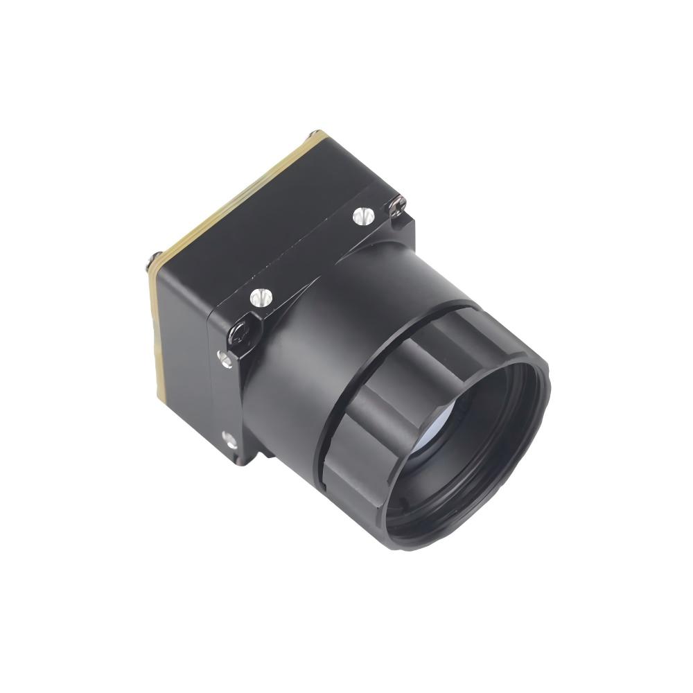
Showcase 1: Uncooled Infrared Mini2 640x512 9mm Drone Thermal Module
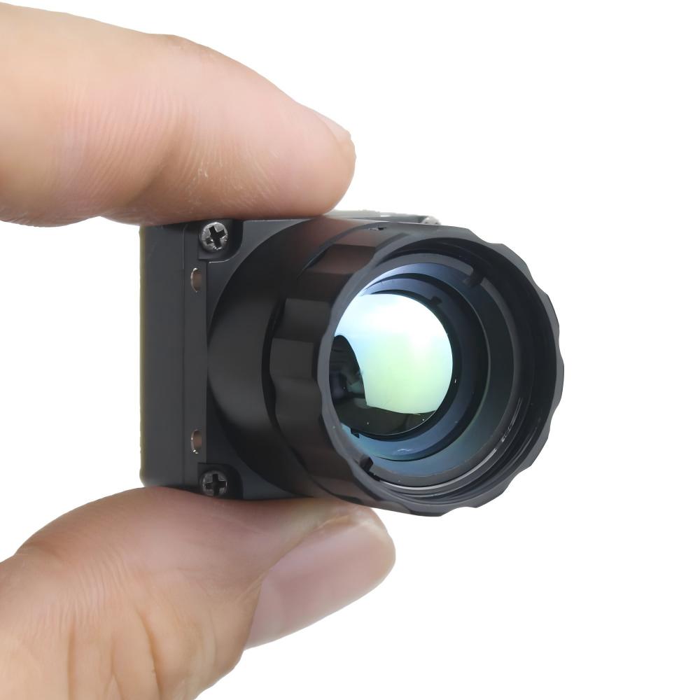
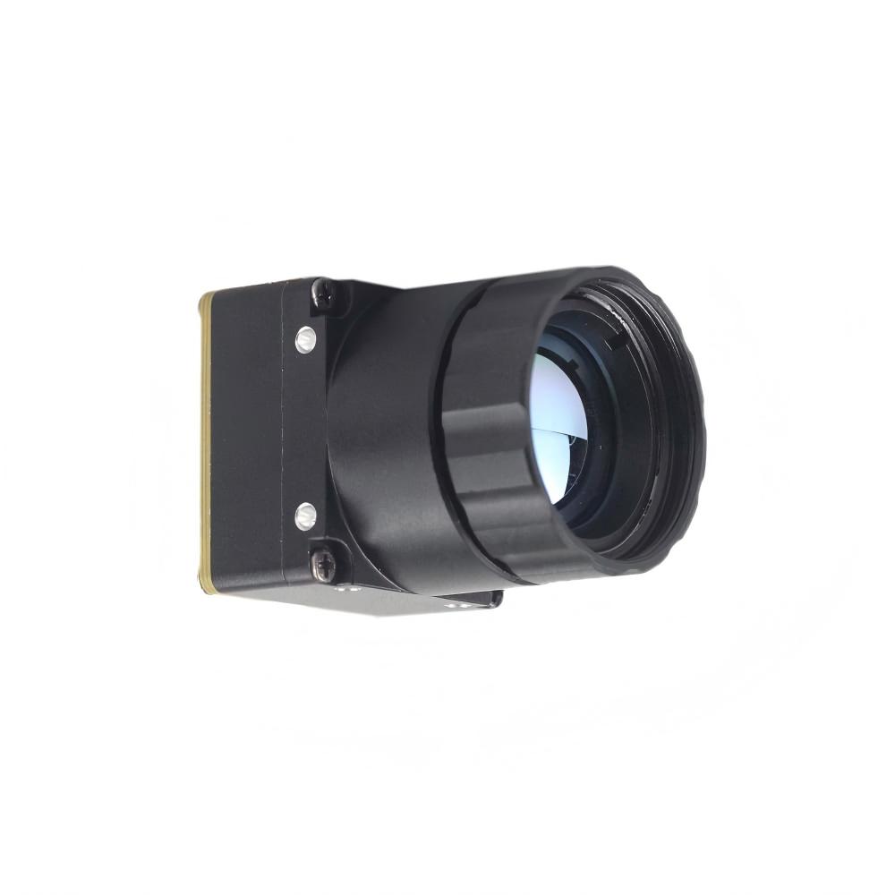
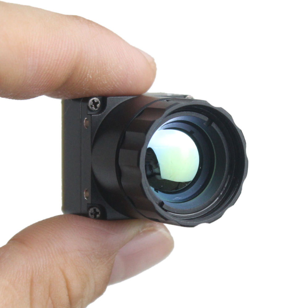
The Mini2 640x512 9mm module is engineered specifically for SWaP-constrained aerial systems, multi-rotor drones, and compact fixed-wing aircraft. Featuring a high-resolution 640x512 VOx microbolometer with a 12µm pixel pitch, this core delivers razor-sharp thermal imagery while maintaining an extraordinarily small footprint and minimal weight profile. Its native MIPI CSI-2 interface provides zero-latency digital video streaming directly to embedded host processors, making it ideal for autonomous navigation, AI object detection, and search-and-rescue payloads.
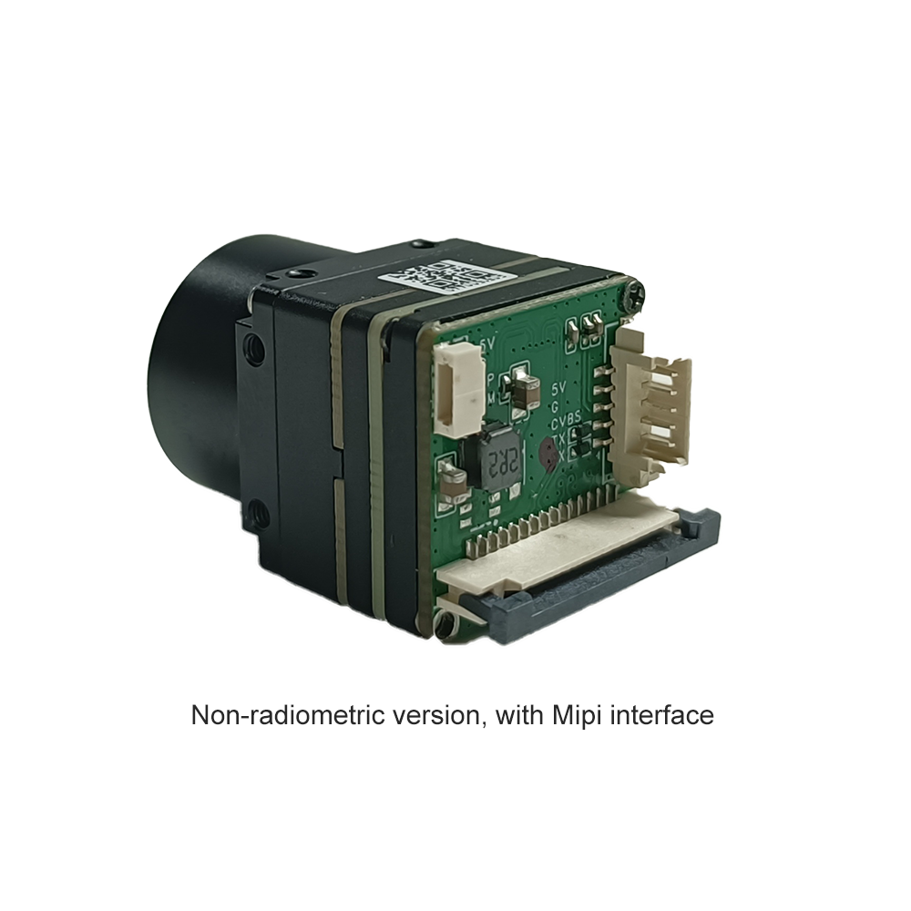
| Resolution & Array | 640 × 512 Focal Plane Array |
| Pixel Pitch | 12 µm Vanadium Oxide (VOx) |
| Thermal Sensitivity (NETD) | < 40 mK (@ f/1.0, 300K, 50Hz) |
| Frame Rate | 50 Hz / 60 Hz Native Real-Time Output |
| Native Interface | Direct MIPI CSI-2 (1-lane or 2-lane D-PHY) |
| Standard Optic | 9 mm Athermalized Germanium Lens (f/1.0, HFOV ~48.7°) |
| Power Consumption | < 0.8 W (Typical Operation) |
| Dimensions & Weight | ~21 mm × 21 mm × 23 mm | < 20 grams (including lens) |
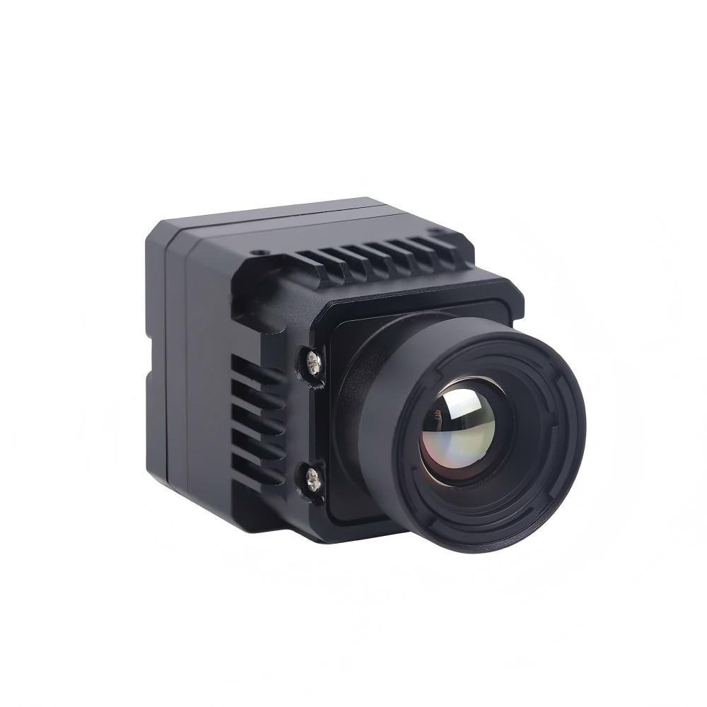
Showcase 2: Purpleriver MD Series 384x288 Thermal Camera Module
The MD Series 384x288 thermal camera module is engineered for industrial precision, critical security surveillance, condition monitoring, and versatile robotic integration. Built on a 12µm uncooled VOx sensor, it delivers outstanding thermal sensitivity and crisp contrast. The standout feature of the MD Series is its multi-interface versatility, supporting MIPI, USB, and analog CVBS outputs on a single platform. This flexibility allows engineers to prototype rapidly using USB and transition seamlessly to low-latency MIPI CSI-2 for volume production.
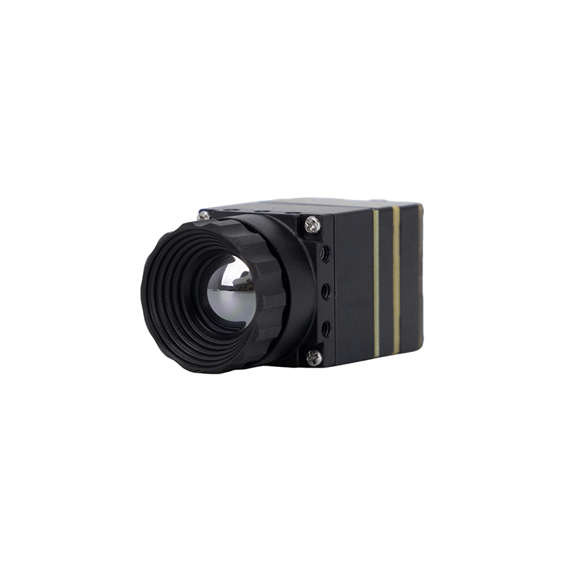
| Resolution & Array | 384 × 288 Focal Plane Array |
| Pixel Pitch | 12 µm VOx Microbolometer |
| Thermal Sensitivity (NETD) | < 40 mK (@ f/1.0, 25°C, 50Hz) |
| Video Interfaces | Multi-Interface: Native MIPI CSI-2 / USB 2.0 / CVBS Analog |
| Measurement Accuracy | Radiometric precision: ±2°C or ±2% reading |
| Customization Capability | Full OEM/ODM customization for lenses, carrier boards, and firmware |
| Power Consumption | < 1.1 W (Full multi-interface transceiver state) |
| Dimensions & Weight | Approx. 25 mm × 25 mm × 26 mm | < 28 grams |
For system integrators weighing architectural tradeoffs across different form factors, resolutions, and payload envelopes, read our detailed guide on selecting uncooled thermal camera modules.
4. UAV SWaP-C Payload Engineering & Aerial Integration
4.1 Thermal Dissipation and Passive Conduction in Enclosed Gimbals
Modern miniature dual-sensor drone gimbals present harsh operating environments: they are tightly sealed to IP65 or IP67 standards to keep out moisture, sand, and dust, leaving zero allowance for active cooling fans or open exhaust vents. In these sealed enclosures, the thermal module's internal electronics (FPGA, ROIC, and power regulators) dissipate between 0.6W and 1.1W of continuous heat.
If unmanaged, this heat builds up inside the housing, raising the temperature of the camera's mechanical structure. This heating can create parasitic thermal gradients across the sensor array, causing non-uniform thermal drift, elevating the NETD noise floor, and degrading overall image contrast. To preserve high thermal sensitivity, payload architects must establish an unbroken passive thermal path:
- ⚙️ Conductive Chassis Coupling: The core's rear housing should be mechanically coupled directly to the gimbal's aluminum frame (such as CNC-machined 6061-T6 aluminum) using a high-performance phase-change material (PCM) or soft thermal gap pad with a thermal conductivity of at least 3.0 W/m·K.
- ⚙️ Thermal Decoupling from Motors: Brushless gimbal motors can run hot under heavy stabilization loads. Use structural thermal insulators—such as ceramic washers or high-temperature FR-4 standoffs—to isolate the optical core from the motor mounts, ensuring motor heat does not sink back into the thermal detector.
- ⚙️ Structural Heat Dissipation: The exterior shell of the gimbal should serve as the primary convective cooling boundary, shedding heat into the propeller downwash during flight.
4.2 Shock, Vibration Isolation, and Aerodynamic Packaging
Drones generate intense high-frequency vibration profiles, primarily driven by motor RPM frequencies (typically 80 Hz to 400 Hz) and aerodynamic turbulence across the airframe. These vibrations can cause optical blur, shake fine-pitch FPC connectors loose, and misalign focus on non-athermalized lenses.
To ensure long-term mechanical reliability:
- ✅ Rugged Fine-Pitch Interconnects: Avoid loose friction-fit zero-insertion-force (ZIF) connectors. Instead, specify locking board-to-board or board-to-FPC headers, such as the ultra-compact, high-retention micro-connectors manufactured by Molex. These connectors maintain pin contact integrity through sustained multi-axis shocks exceeding 50G.
- ✅ Optical Element Locking: Lens assemblies must be factory-aligned and secured using low-outgassing structural thread adhesives (such as Loctite 222 or specialized UV-curing epoxies) to prevent optical drift over repeated thermal and vibration cycles.
- ✅ Athermalized Optics: Uncooled LWIR lenses must maintain crisp optical focus across wide temperature ranges (-40°C to +80°C). Optomechanical athermalization pairs optical elements with housing barrels made from materials with opposing coefficients of thermal expansion (CTE), maintaining sharp focus automatically without requiring bulky, power-hungry mechanical autofocus mechanisms.
4.3 Radiometric vs. Non-Radiometric Firmware Implementations
When selecting a 640x512 MIPI thermal module, system architects must evaluate whether their mission requires true radiometric temperature data or optimized visual tracking:
| Parameter | Radiometric Firmware | Non-Radiometric (Visual Imaging) |
|---|---|---|
| Output Data | Linearized Kelvin temperatures (14/16-bit integer) | Dynamic contrast-stretched imagery (8/14-bit) |
| Factory Calibration | Multi-temperature blackbody calibration curves | Two-point uniform field calibration |
| Primary Mission | Grid inspection, solar farm maintenance, wildfire detection | ISR flight, tactical night vision, hunter-killer target loops |
| Processing Pipeline | Atmospheric, emissivity, and distance compensation | Edge enhancement, local tone mapping, histogram equalizing |
5. Edge AI Pipelines: Processing 640x512 Thermal Streams on Linux/RTOS
5.1 V4L2 Driver Framework and Device Tree Overlays
To integrate a 640x512 MIPI thermal module on embedded Linux platforms (such as NVIDIA JetPack, Yocto Project, or custom Linux distributions), the camera is implemented as a V4L2 subdevice. The system controls the core via an I2C control bus and captures streaming video across the MIPI CSI-2 interface.
The hardware architecture is defined using a Device Tree Overlay (DTS) file. The overlay maps the peripheral connections, sets the internal reference clock frequencies, configures the hardware reset GPIOs, and assigns the MIPI CSI-2 data lanes:
// Purpleriver Mini2 640x512 MIPI CSI-2 Device Tree Snippet
/dts-v1/;
/plugin/;

/ {
    fragment@0 {
        target = <&i2c_bus1>;
        __overlay__ {
            #address-cells = <1>;
            #size-cells = <0>;

            thermal_cam: camera_core@38 {
                compatible = "purpleriver,mini2-640";
                reg = <0x38>;
                status = "okay";

                clocks = <&bpmp_clks 12>;
                clock-names = "extcore_clk";
                reset-gpios = <&gpio 21 0>;

                port {
                    cam_out: endpoint {
                        remote-endpoint = <&csi_in_ep>;
                        clock-lanes = <0>;
                        data-lanes = <1>;
                        link-frequencies = /bits/ 64 <240000000>;
                        bus-type = <4>; /* MIPI CSI-2 D-PHY */
                    };
                };
            };
        };
    };
};
The kernel driver exposes controls for setting NUC mode, setting color palettes, and updating integration times via standard V4L2 IOCTL interfaces. Video frames stream directly into DMA-allocated ring buffers mapped through V4L2_MEMORY_MMAP or V4L2_MEMORY_DMABUF, providing clean, zero-copy user-space access.
5.2 14-Bit Raw to 8-Bit Dynamic Range Compression (AGC & CLAHE)
Microbolometers natively capture broad thermal dynamic ranges, outputting 14-bit or 16-bit raw digital signals (spanning 16,384 to 65,536 discrete intensity steps). However, standard display systems and edge neural networks operate on 8-bit image formats ([0, 255]).
Applying naive linear quantization across a broad 14-bit input compresses subtle thermal differences into negligible variations, obscuring low-contrast targets like humans in warm environments. To maintain target clarity, modern embedded pipelines use dynamic range compression algorithms:
- ⚙️ Contrast-Limited Adaptive Histogram Equalization (CLAHE): CLAHE operates over local contextual tiles across the thermal frame rather than equalizing the entire scene uniformly. It applies a clip limit to local histograms to prevent over-amplifying sensor noise in low-gradient areas like flat skies, calm water, or smooth terrain.
- ⚙️ Digital Detail Enhancement (DDE): The raw thermal frame is split into a low-frequency base layer (representing overall scene temperatures) and a high-frequency detail layer (containing sharp silhouette edges, textures, and thermal gradients). The high-frequency detail layer is amplified, recombined with the equalized base layer, and mapped into the target 8-bit space, preserving critical edge definition.
For additional perspectives on image processing and diverse deployment scenarios for thermal sensors across modern industry, read our overview of everyday and practical applications of thermal cameras.
5.3 Real-Time TensorRT and Deep Learning Inference at the Edge
Streaming a 640x512 thermal feed via MIPI directly into unified memory on an embedded edge compute module (such as the NVIDIA Jetson Orin platform) provides significant advantages for running deep learning object detection pipelines. High-speed CUDA kernels preprocess the incoming 14-bit frames—handling CLAHE compression, normalization, and color mapping—directly inside GPU memory without round-tripping data through host RAM.
Once converted to FP16 or INT8 tensors, the thermal frames feed directly into neural networks optimized with NVIDIA TensorRT—such as YOLOv8s, YOLOv10, or RT-DETR. Because long-wave infrared sensors capture raw thermal emissions rather than reflected visible light, the inference pipeline performs consistently in total darkness, through dense smoke, and amid direct optical glare. Running a TensorRT-optimized INT8 YOLO model on a 640x512 stream on an Orin Nano executes in approximately 4 to 6 milliseconds, maintaining an unbroken, high-confidence target tracking loop at 50 frames per second.
6. Electrical, Pinout, and Mechanical Interfacing Standards
Designing high-speed carrier boards for a 640x512 MIPI thermal module requires careful high-frequency PCB layout and stable, low-noise power distribution. Noise on digital lines can easily couple into the microbolometer's sensitive analog readout circuitry, directly degrading the sensor's NETD performance.
| Pin Range | Signal Designation | Signal Type | Routing & Layout Engineering Guidance |
|---|---|---|---|
| Pin 1, 4 | VDD_IN (3.3V - 5.0V) | Power Rail | Power with low-noise LDO regulator (<15µV RMS). Add 0.1µF and 10µF bypass caps near pins. |
| Pin 2, 3 | GND | Reference Ground | Connect to an unbroken ground return plane directly under high-speed differential pairs. |
| Pin 5, 6 | I2C_SDA / I2C_SCL | Open Drain Control | Standard I2C bus (supports 400kHz Fast-mode). Place external 2.2kΩ pull-up resistors to 1.8V/3.3V. |
| Pin 7, 8 | RESET_N / TRIG_IN | CMOS Digital I/O | Active-low hardware reset; optional external hardware frame-sync pulse input for stereoscopic capture. |
| Pin 10, 11 | MIPI_CLK_P / N | Differential Pair | 100Ω ± 10% differential impedance. Keep intra-pair trace length matching within 0.15mm. |
| Pin 13, 14 | MIPI_DATA0_P / N | Differential Pair | 100Ω ± 10% differential impedance. Route over continuous ground with zero split planes. |
| Pin 16, 17 | MIPI_DATA1_P / N | Differential Pair | Optional second MIPI data lane for lower clock frequencies across long FPC runs. |
Key routing rules for embedded carrier boards:
- ⚙️ Strict Impedance Control: All MIPI CSI-2 differential traces must be routed with tightly controlled 100Ω differential impedance (±10%). Avoid using vias where possible; when layer transitions are required, place complementary ground stitching vias immediately adjacent to the signal vias.
- ⚙️ Trace Skew Minimization: Intra-pair trace skew (between the P and N signals) must not exceed 0.15mm (representing ~1 picosecond of skew). Inter-pair skew between the clock lane and data lanes should remain below 0.5mm.
- ⚙️ Analog Power Supply Rail: Never power uncooled thermal camera cores directly from an unfiltered switching buck-boost DC/DC converter. Switching ripple on the primary supply line can manifest as periodic horizontal banding across the thermal video output. Always place an ultra-low-noise linear Low-Dropout regulator (LDO) upstream of the module.

7. Industrial Engineering Technical FAQ
How do I integrate a 640x512 MIPI thermal module with Linux platforms like Raspberry Pi or Jetson?
At the software level, write and compile a Device Tree Overlay (DTS) defining the camera's I2C control address (typically 0x38), power enable GPIOs, reference clock speed, and D-PHY lane topology (1 clock lane, 1 or 2 data lanes at 240MHz link frequency). Next, compile the module's V4L2 subdevice kernel driver into the kernel. Once loaded, Linux will expose the camera stream at /dev/videoX. Applications can then capture the raw 14-bit thermal feed at 50Hz via V4L2 APIs, GStreamer pipelines, or native OpenCV loops using memory-mapped buffers (V4L2_MEMORY_MMAP) for zero-copy efficiency.
Why should I upgrade from 256x192/384x288 sensors to a 640x512 12μm MIPI thermal core for drones and custom optics?
Furthermore, modern deep learning vision models (such as YOLOv8 and RT-DETR) require sufficient pixels across a target silhouette to classify objects reliably; the richer pixel density of a 640x512 array substantially reduces false negatives at long range. Finally, the modern 12µm pixel pitch enables a 40% reduction in the physical size and weight of Germanium objective lenses compared to older 17µm sensors with equivalent fields of view, reducing overall payload weight below 20 grams to maximize drone flight endurance.
What is the difference between non-uniformity correction (NUC) and bad pixel replacement (BPR)?
Non-Uniformity Correction (NUC): Due to microscopic fabrication tolerances, individual microbolometers exhibit slight variations in electrical resistance, temperature coefficients (TCR), and thermal dissipation. Viewing a completely uniform thermal scene can therefore produce fixed-pattern noise (FPN) that looks like a static haze across the image. NUC applies two-point calibration matrices (gain and offset correction) across every pixel to equalize response. These corrections are updated in real time via an internal mechanical shutter or shutterless algorithmic compensation.
Bad Pixel Replacement (BPR): A 640x512 sensor array contains 327,680 microscopic bridge membranes. Inevitably, a tiny fraction of these pixels (<0.5%) will be non-responsive (dead pixels), stuck at full saturation, or exhibit excessive noise beyond calibration limits. Because standard gain/offset math cannot fix an unresponsive pixel, BPR algorithms step in. The core stores a factory-mapped dead-pixel table in non-volatile flash memory and replaces defective pixel values on the fly by interpolating values from surrounding, functional neighbor pixels (using median or gradient-weighted averaging).
Can MIPI CSI-2 thermal modules stream across long cable runs inside larger industrial platforms?
To deploy a MIPI thermal module across longer distances—such as along robotic arms, tall security masts, or throughout large industrial vehicles (1 to 15 meters away from the central compute engine)—engineers use industrial SerDes (Serializer/Deserializer) bridging chipsets. A compact serializer board (such as Texas Instruments FPD-Link III/IV or Analog Devices GMSL2) is integrated directly at the camera module output. The serializer merges the MIPI data lanes, clock, and bidirectional I2C control signals onto a single flexible 50Ω coaxial cable or shielded twisted pair. At the host processor side, a companion deserializer IC unpacks the stream back into native MIPI CSI-2 and routes it to the SoC's camera inputs with zero noticeable latency and high immunity to industrial EMI.
📚 References & Further Reading
- Industry Standard: High-reliability micro-interconnect specifications for embedded payloads by Molex
- Industry Standard: Embedded AI computing platforms and hardware CSI-2 interfacing on NVIDIA Jetson
- Related Guide: Engineering architecture and core tradeoffs in Selecting Uncooled Thermal Camera Modules
- Related Guide: Foundational optical conversions and the Physical Principles of Thermal Imaging
- Related Guide: Operational use cases and Everyday and Practical Applications of Thermal Cameras