
Thermal Camera Guide: How to Choose, Integrate, and Maximize AI Infrared Performance
2026年10月16日
Best Thermal Imager Guide: Budget Gadgets vs. Industrial AI LWIR Modules
2026年10月19日
Thermal Imaging Camera Guide: Resolution, Sensor Specs & Core Modules Explained
Thermal imaging technology has migrated rapidly from defense-grade surveillance labs into the core of commercial robotics, automated predictive maintenance, uncrewed aerial vehicles (UAVs), and inline industrial inspection. At the heart of this shift is the transition from bulky, monolithic handheld systems to SWaP-optimized (Size, Weight, Power, and Cost) long-wave infrared (LWIR) core modules. However, modern system architects and OEM engineers frequently face a critical bottleneck: deciphering misleading consumer-grade datasheets where interpolated resolutions, high thermal noise thresholds, and frame rate throttling hide severe integration limitations. Selecting an industrial-grade thermal imaging camera demands a rigorous evaluation of sensor physics, focal plane array (FPA) microbolometer compositions, optical transmission trade-offs, and downstream embedded edge computing constraints.
Building a dependable, high-precision thermographic platform requires understanding that raw sensor resolution is meaningless without high thermal sensitivity (Noise Equivalent Temperature Difference, or NETD) and properly calibrated spatial resolution (Instantaneous Field of View, or IFOV). Whether identifying microscopic solder bridging on high-density PCBs, monitoring thermal dissipation gradients across battery cells in electric vehicles, or tracking structural integrity from a drone payload at 100 meters altitude, optical tolerances and raw radiometric streaming must be balanced against mechanical and compute envelopes. This technical guide breaks down the core physics, detector materials, optical design parameters, and hardware integration pipelines required to engineer dependable thermal vision systems.
Table of Contents
- 👉 1. The Physics of Thermal Imaging: Radiation, Emissivity & Radiometry
- 👉 2. Sensor Architectures: Uncooled Microbolometers
- 👉 3. Spatial Resolution, Optics & DRI Range Dynamics
- 👉 4. Embedded Integration, ISP Pipelines & Edge AI
- 👉 5. OEM Core Module Performance Showcase
- 👉 6. Industrial Thermal Imaging Engineering FAQ
1. The Physics of Thermal Imaging: Radiation, Emissivity & Radiometry
A thermal imaging camera operates on fundamentally different physical principles than visible light imaging systems. While standard charge-coupled device (CCD) and complementary metal-oxide-semiconductor (CMOS) sensors register reflected visible electromagnetic radiation within the narrow band of 0.38 to 0.75 micrometers (µm), thermal sensors detect emitted radiation across the infrared spectrum. This emitted energy is governed by fundamental thermodynamic laws, primarily Planck's Radiation Law, Wien's Displacement Law, and the Stefan-Boltzmann Law.
The total radiant emittance from an ideal blackbody surface across all wavelengths is expressed mathematically by the Stefan-Boltzmann Law:
W = ε · σ · T4
Where W represents the total hemispherical radiant emittance in Watts per square meter (W/m²), ε is the surface emissivity of the observed material, σ is the Stefan-Boltzmann constant (approximately 5.670 × 10⁻⁸ W/(m²·K⁴)), and T is the absolute thermodynamic temperature of the object expressed in Kelvin (K). Because emitted radiant energy scales with the fourth power of absolute temperature, even subtle variations in surface temperature produce measurable shifts in total emitted photon flux.
THERMAL IMAGING REAL-TIME VIDEO
For industrial monitoring, terrestrial robotics, and aerial inspections targeting ambient operating conditions between -40°C and +500°C (-40°F to +932°F), Planck's spectral distribution shows that peak radiant emission resides within the Long-Wave Infrared (LWIR) atmospheric transmission window, spanning from 8.0 to 14.0 µm. Wien's Displacement Law confirms that a blackbody radiator at nominal room temperature (300 Kelvin) radiates peak spectral emittance at approximately 9.66 µm. Within this specific spectral band, atmospheric attenuation caused by airborne water vapor (H₂O) and carbon dioxide (CO₂) absorption molecules is minimized. This low atmospheric attenuation allows uncooled thermal sensors to detect clear thermal signatures across open air without requiring active external infrared illumination.
A central challenge in quantitative thermography is the divergence of real-world materials from theoretical blackbodies. A blackbody absorbs all incident radiation and re-emits it with perfect efficiency (ε = 1.0). Real-world targets are classified as "graybodies" or selective emitters, governed by Kirchhoff’s Law of Thermal Radiation:
ε + ρ + τ = 1
In this relationship, ε represents emissivity, ρ represents reflectivity, and τ represents transmissivity. In most practical industrial inspection scenarios, the targets of interest—such as painted machine casings, electrical motor housings, insulated piping, and structural earth—are completely opaque to LWIR radiation, meaning transmissivity τ equals zero. As a result, the conservation equation simplifies directly to:
ε + ρ = 1
This thermodynamic relationship introduces significant engineering implications. High-emissivity targets (such as non-glossy electrical tape, matte black paint, anodized aluminum, and human skin; where ε ranges from 0.92 to 0.98) emit infrared flux directly proportional to their kinetic surface temperature. Conversely, low-emissivity, highly specular surfaces (such as unoxidized bare copper traces on printed circuit boards, machined aluminum heatsinks, or polished stainless-steel pipework; where ε is often below 0.15) emit very little intrinsic thermal energy. Instead, they act as infrared mirrors, reflecting surrounding ambient radiation into the detector lens.
If an uncalibrated thermal imaging camera inspects a polished metallic surface without compensating for ambient reflected temperature (T_refl) and true target emissivity, the resulting output will display the thermal reflection of the surrounding room or operator rather than the component's true thermodynamic state. Industrial-grade thermographic engines account for this by incorporating multi-parameter radiometric solver pipelines. These solvers recalculate the temperature values across every pixel matrix by factoring in target emissivity, background reflection, ambient atmospheric temperature, relative humidity, and target-to-lens physical distance.
System architects must also maintain a clear distinction between qualitative thermography and quantitative radiometry:
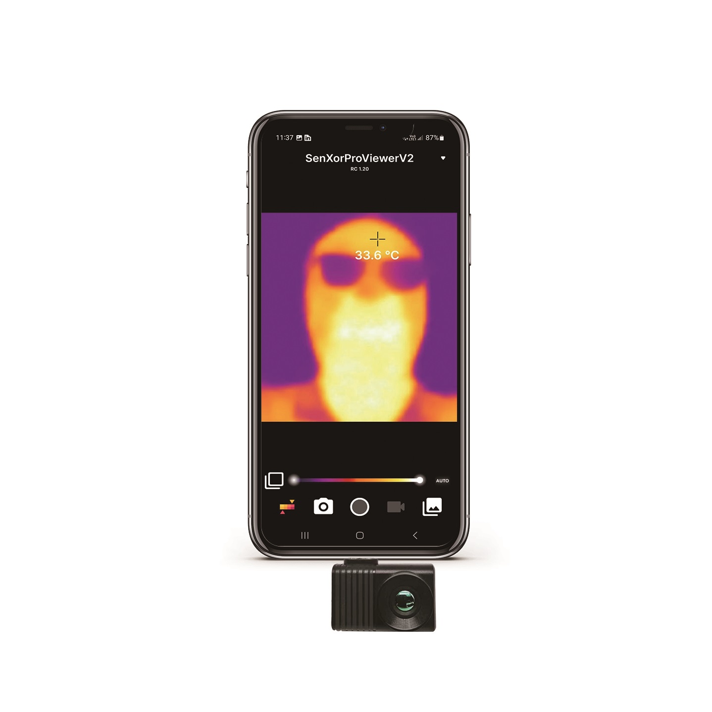
- ⚙️ Qualitative Thermography (Imaging Output): The sensor processes thermal radiation solely to map relative temperature differentials across the field of view. The resulting output is converted into an 8-bit visual false-color palette (such as Ironbow, Rainbow, White Hot, or Black Hot) optimized for human perceptual tracking. While qualitative imagery is valuable for navigation and obstacle avoidance, individual pixel values represent relative thermal contrast rather than calibrated engineering units.
- ⚙️ Quantitative Radiometry (Precision Measurement): Every individual microbolometer pixel on the Focal Plane Array measures and stores a discrete, calibrated 14-bit or 16-bit raw digital number (DN). This raw value maps directly to an absolute temperature calculation in Celsius, Fahrenheit, or Kelvin through a dedicated polynomial calibration equation. Quantitative radiometry is essential for edge computing tasks, automated anomaly detection, inline manufacturing validation, and predictive maintenance alerting where automated logic decisions rely on precise physical thresholds.
2. Sensor Architectures: Uncooled Microbolometers
Thermal infrared imaging systems fall broadly into two primary engineering classifications: cooled photon detectors and uncooled thermal detectors. Cooled systems typically utilize narrow-bandgap semiconductor materials such as Indium Antimonide (InSb) or Mercury Cadmium Telluride (MCT) operating in the Mid-Wave Infrared (MWIR, 3.0 to 5.0 µm) spectrum. These detectors require integrated cryocoolers (such as closed-cycle Stirling engines) to chill the focal plane array down to cryogenic temperatures (approximately 77 Kelvin / -196°C) to suppress thermally generated dark currents. While cooled systems offer extraordinary sensitivity and ultra-high frame capture rates, their immense cost, bulky form factors, high power draw (often 10W to 50W), and finite cryocooler mechanical lifetimes make them unsuitable for cost-sensitive commercial integration, compact drone payloads, and long-term unattended monitoring.
In contrast, modern commercial and industrial LWIR systems rely on uncooled microbolometer Focal Plane Arrays (FPAs). An uncooled microbolometer consists of a two-dimensional grid of microscopic detector pixels fabricated directly over a silicon Readout Integrated Circuit (ROIC) via surface micromachining MEMS (Micro-Electro-Mechanical Systems) techniques. Each individual pixel features a thin absorber membrane suspended above the underlying silicon substrate by micro-machined thermal isolation bridges or legs. This suspended architecture creates an isolated thermal mass with exceptionally high thermal resistance (R_th) to the substrate, housed within a permanent wafer-level vacuum package (WLP) to eliminate convective heat dissipation.
When incident long-wave infrared radiation strikes the microbolometer pixel membrane, the absorber material captures the photon flux, raising the temperature of the suspended membrane. This localized temperature shift directly alters the electrical resistance of the thin-film thermistor material embedded within the membrane structure. The rate of this resistance variation relative to temperature is defined as the Temperature Coefficient of Resistance (TCR), designated as α:
α = (1 / R) · (dR / dT)
The underlying ROIC applies a stabilized electrical bias voltage or current across the pixel array, sequentially measuring the resulting changes in voltage or current column-by-column and row-by-row. These analog signals are then digitized via high-resolution on-chip analog-to-digital converters (ADCs), outputting raw 14-bit or 16-bit radiometric values for every frame cycle.
The performance of an uncooled microbolometer FPA is heavily dictated by the chemical composition of the thermistor thin film. The industrial thermal imaging camera market is dominated by two primary material technologies: Vanadium Oxide (VOx) and Amorphous Silicon (a-Si).
| Specification / Parameter | Vanadium Oxide (VOx) | Amorphous Silicon (a-Si) | Engineering System Impact |
|---|---|---|---|
| TCR (Temperature Coefficient) | -2.0% to -3.0% per Kelvin | -2.0% to -2.5% per Kelvin | Higher TCR enables superior dynamic electrical response per unit of absorbed heat. |
| Typical System NETD | < 35 mK to 50 mK | 50 mK to 80 mK | VOx resolves minute temperature differences across scenes with lower intrinsic spatial noise. |
| Thermal Time Constant (τ) | Fast (8 ms to 12 ms) | Moderate (12 ms to 16 ms) | Faster response mitigates thermal image blur and trailing during dynamic drone motion. |
| 1/f (Flicker) Noise Profile | Extremely Low | Moderate to High | VOx maintains superior radiometric baseline stability over shifting sensor temperatures. |
| Manufacturing Complexity | Specialized MEMS thin-film deposition | Standard Silicon CMOS compatibility | a-Si can offer lower volume costs, but VOx remains the preferred standard for precision tasks. |
Vanadium Oxide is widely recognized as the superior material for demanding industrial, robotic, and aerial applications. Due to its combined high TCR and low 1/f electrical noise characteristics, VOx microbolometers achieve exceptional Noise Equivalent Temperature Difference (NETD) ratings. NETD represents the fundamental figure of merit for thermal camera sensitivity, quantifying the minimum temperature delta at the target required to produce an electrical signal-to-noise ratio of unity (SNR = 1) at the sensor output. Formally, NETD is expressed as:
NETD = V_n / (dV_s / dT)
Where V_n is the root-mean-square (RMS) noise voltage of the detector system, and (dV_s / dT) represents the sensor signal output change per unit change in target scene temperature. A lower NETD figure, expressed in millikelvins (mK), directly equates to higher sensitivity:
- ⚙️ NETD > 60 mK: Common in entry-level, consumer-grade thermal units. Images exhibit noticeable high-frequency spatial noise (visual grain), masking subtle thermal anomalies such as subsurface building moisture, delamination in composite aero-structures, or faint pipeline leakage.
- ✅ NETD ≤ 40 mK to 50 mK: The standard for robust industrial thermography. Effectively renders minute heat transfers across loaded electronics and mechanical bearings under variable ambient operational conditions.
- ✅ NETD < 30 mK to 35 mK: High-end research and tactical grade. Delivers crisp radiometric delineation of low-thermal-contrast targets, such as buried underground infrastructure or landmines concealed beneath surface soil.
Alongside material chemistry, pixel pitch scaling plays a decisive role in microbolometer development. The industry has largely transitioned from legacy 17 µm and 25 µm pixel geometries to modern 12 µm architectures. Reducing pixel pitch from 17 µm to 12 µm decreases the total surface area of a single pixel by approximately 50%. This footprint reduction enables sensor manufacturers to dramatically shrink the overall physical dimensions of the FPA for a given spatial resolution, which in turn reduces the diameter of the required optical elements.
Because smaller FPAs project a smaller image circle, the front optical elements can be designed with significantly smaller physical apertures while maintaining an identical optical speed (F-number). This reduction in glass diameter lowers payload weight and production costs, making 12 µm VOx arrays the preferred configuration for SWaP-constrained drone payloads and compact robotic arms.
3. Spatial Resolution, Optics & DRI Range Dynamics
A thermal imaging camera cannot rely on standard optical glasses like N-BK7 or fused silica, as these common optical materials become opaque to electromagnetic radiation at wavelengths beyond 2.5 µm. Capturing photons across the 8.0 to 14.0 µm LWIR spectrum requires exotic optical materials capable of high transmission and minimal internal absorption.
The most common material for LWIR refractive lenses is monocrystalline Germanium (Ge). Germanium features an exceptionally high refractive index (n ≈ 4.00 at 10 µm), enabling optical designers to engineer high-aperture lenses (such as F/1.0 and F/1.1) with minimal optical aberrations using fewer lens elements. However, Germanium exhibits significant trade-offs: it is mechanically heavy, expensive, and subject to thermal runaway. When the internal temperature of a Germanium optic rises above 70°C to 80°C, its free-electron density increases drastically, turning the optic opaque to infrared light.
To overcome these challenges, optical engineers use specialized Chalcogenide glasses (such as Ge-Sb-Se or GASIR formulations). Chalcogenide materials can be precision molded into complex aspheric lens profiles, significantly reducing optical element count and weight. Crucially, Chalcogenide glass possesses a very low thermo-optic coefficient (dn/dT), making it an excellent medium for passive athermalization. Athermalized lenses maintain precise mechanical focus across broad ambient temperature spans (from -40°C to +80°C) without requiring motorized focus compensation mechanics. For custom optical assemblies and diamond-turned LWIR lens components, developers often partner with precision optical fabricators such as Jinde to maintain strict wavefront tolerances and maximize sensor throughput.
Evaluating the optical performance of a thermal imaging camera requires calculating its Instantaneous Field of View (IFOV). IFOV describes the angular cone of vision captured by an individual detector pixel, measured in milliradians (mrad):
IFOV = (p / f)
Where p represents the physical pixel pitch of the microbolometer detector (e.g., 0.012 mm for a 12 µm sensor) and f is the focal length of the optical lens assembly in millimeters. To determine the spatial spot size (S) projected by a single pixel onto an inspection target at an operational distance (D), the calculation expands to:
S = IFOV · D = (p / f) · D
However, an essential distinction must be made between theoretical spatial detection (IFOV) and true measurement accuracy, known as Measurement IFOV (M-IFOV). Due to optical diffraction limits, optical point spread functions (PSF), atmospheric scattering, and electronic pixel crosstalk within the ROIC, a single pixel cannot accurately measure the absolute temperature of a target. To achieve precise radiometric measurement (where recorded digital counts accurately reflect calibrated target temperature), the target must completely cover a cluster of multiple pixels on the FPA.
As a rule of thumb, M-IFOV requires an optical footprint of at least 3 × 3 to 4 × 4 contiguous pixels across the critical dimension of the target. If an engineer attempts to measure a surface-mount electronic component measuring 2 mm × 2 mm using an optical system that projects a 1-pixel IFOV of 2 mm at that distance, the resulting radiometric reading will suffer from severe slit-response dilution. The measured value will represent an inaccurate blend of the component's true heat signature and the cooler surrounding PCB substrate.
For surveillance, perimeter security, and drone payloads, operational range performance is characterized using the classical Johnson Criteria for Detection, Recognition, and Identification (DRI):
- ⚙️ Detection (1.5 line pairs / ~2 to 3 pixels on target): The operator or automated system can discern that a distinct thermal anomaly or target exists against the background environment.
- ⚙️ Recognition (6.0 line pairs / ~6 to 8 pixels on target): The system can classify the general category of the target (e.g., discerning a commercial vehicle from a human pedestrian, or distinguishing a structural pylon from a tree trunk).
- ⚙️ Identification (12.0 line pairs / ~12 to 16 pixels on target): The system resolves fine detail on the target (e.g., confirming whether a person is carrying an object, or identifying the exact chassis model of a monitored vehicle).
Upgrading a thermal payload from a 256 × 192 FPA to a 640 × 512 FPA increases the total active pixel count from 49,152 to 327,680 pixels—a 6.6-fold increase. This allows the thermal imaging camera to achieve identical DRI distances using wider field-of-view optics, significantly expanding the monitored ground footprint per flight pass, or to extend target recognition distances when paired with narrow telephoto optics.
4. Embedded Integration, ISP Pipelines & Edge AI
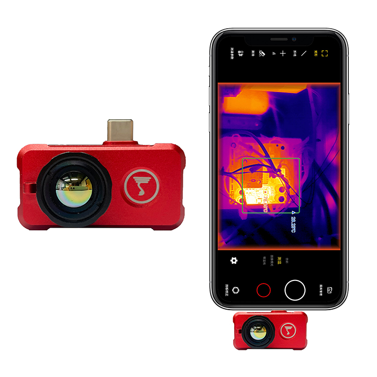
While handheld, all-in-one thermal diagnostic tools serve maintenance technicians well for intermittent manual inspections, they present severe architectural bottlenecks when integrated into autonomous robotics, drone gimbals, machine vision sorting lines, and OEM monitoring enclosures:
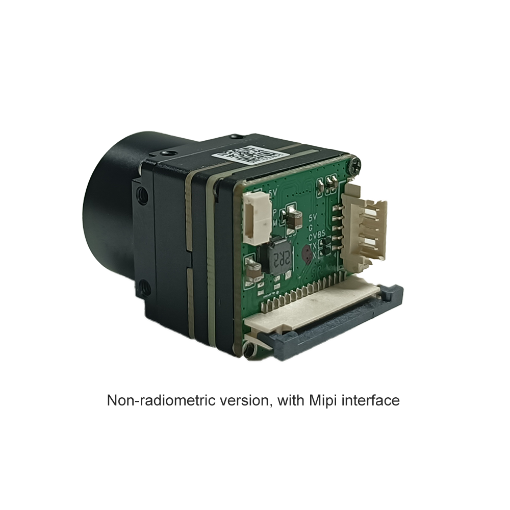
- ⚙️ Size, Weight, and Power (SWaP) Bottlenecks: Handheld units house internal displays, physical control interfaces, internal battery packs, and heavy structural plastics. A typical handheld tool weighs between 400g and 1000g and consumes significant operating power. In contrast, an uncooled LWIR core module strips away all non-essential hardware, providing an ultra-compact footprint (often down to 21 mm × 21 mm) that weighs less than 30 grams and consumes roughly 1.0W to 1.5W of power.
- ⚙️ Data Pipeline Restrictions: Handheld instruments are closed processing environments. They output compressed 8-bit visual streams (such as MP4 or JPEG) over HDMI or USB, where raw radiometric sensor outputs are permanently mapped to fixed false-color palettes. This lossy processing prevents external host microprocessors from accessing true, floating-point radiometric matrices, making downstream computer vision, statistical anomaly flagging, and edge AI inference impossible.
- ⚙️ Interface Rigidity: Handheld devices lack low-latency embedded digital interconnects. Integrating them into an automated industrial workflow requires cumbersome physical adaptors and custom display-scraping scripts. Compact OEM cores, by comparison, expose native interfaces such as MIPI-CSI, parallel CMOS, USB 2.0/3.0, and standard UART/RS-232 serial control buses, enabling direct board-to-board integration.
To examine the architectural blueprints and hardware interface options for embedding uncooled thermal cores into complex robotic and industrial assemblies, developers should review our engineering guide on comprehensive camera module integration, analyze our technical review on high-resolution core modules for aerial payloads, or consult our specialized documentation on micro-module embedded development.
Deploying raw microbolometer data downstream requires a dedicated thermal Image Signal Processor (ISP) pipeline. Raw uncooled microbolometer sensor outputs exhibit severe non-uniformity and drift caused by changing ambient operating conditions, internal electronic heat dissipation, and micro-scale manufacturing variances across the individual pixel membranes. The thermal ISP pipeline corrects these distortions deterministically across several operational stages:
- ⚙️ Non-Uniformity Correction (NUC): Each pixel possesses an individualized response gain and voltage offset baseline. Factory calibration generates comprehensive 2-point pixel correction matrices, normalizing output across the array to ensure consistent temperature reporting.
- ⚙️ Bad Pixel Replacement (BPR): Micro-scale MEMS yields can result in a small percentage of dead, saturated, or noisy pixels. The ISP identifies these coordinates from a factory-flashed bad-pixel map and interpolates their values in real time based on surrounding operational pixels.
- ⚙️ Flat-Field Correction (FFC): As internal housing temperatures fluctuate during operation, the sensor's baseline drift introduces spatial fixed-pattern noise (FPN), commonly appearing as vertical striping across the image. An integrated electromechanical shutter drops into the optical path for a fraction of a second, presenting an optically uniform blackbody surface to the sensor. The ISP recalibrates its offset coefficients against this flat field, clearing the thermal image of drift artifacts. Modern advanced cores can also run scene-based non-uniformity correction (SBNUC) algorithms to minimize physical shutter actuations.
- ⚙️ Spatial and Temporal Noise Reduction: 3D temporal recursive filters (3D-DNR) and bilateral spatial filters suppress high-frequency thermal noise without blurring moving targets or softening critical edge boundaries.
- ⚙️ Dynamic Range Compression & Digital Detail Enhancement (DDE): Uncooled LWIR detectors capture 14-bit or 16-bit radiometric raw dynamic ranges (representing up to 65,536 discrete digital levels). Standard visual displays only render 8-bit grayscale or color channels (256 levels). If a wide thermal scene (spanning a range of -20°C to +150°C) is linearly mapped down to 8 bits, small temperature differentials (such as a 0.5°C anomaly on a cold bearing) will compress into a single digital display level, disappearing from view. Advanced ISP algorithms utilize localized histogram equalization and edge-preserving filtering to separate low-frequency background temperature fields from high-frequency structural surface details, boosting subtle thermal details into crisp visual contrast.
For modern edge AI and robotic vision architectures, thermal imaging modules are commonly integrated with compact embedded compute platforms like NVIDIA Jetson modules (including the Orin Nano, Orin NX, and AGX Orin families). Under this system topology, the camera core communicates over high-speed USB 3.0 (UVC class) or direct multi-lane MIPI-CSI buses via native Linux Video4Linux2 (V4L2) driver architectures.
The host pipeline frequently forks the incoming sensor stream into two synchronized threads: an 8-bit YUYV/RGB feed passed directly to an operator display or ground control station, and a concurrent 14-bit or 16-bit radiometric Y16 stream. Deep neural networks (such as YOLOv8, RT-DETR, or custom segmentation networks optimized using NVIDIA TensorRT) ingest this high-bit-depth array. By running inference directly on uncompressed radiometric data, the neural network evaluates true absolute energy fluxes across the monitored scene, enabling reliable, automated target classification regardless of the display palette or false-color mapping settings chosen by an operator.
5. OEM Core Module Performance Showcase
Selecting the optimal thermal imaging camera hardware requires aligning operational requirements with field-tested micro-core performance specifications. Below are two industry-standard uncooled LWIR thermal camera modules engineered specifically for integration into autonomous drones, industrial robotics, security gimbals, and handheld instrumentation assemblies.
| Architectural Specification | Mini 256 LWIR Camera Module | Mini 640 LWIR USB Core Module |
|---|---|---|
| Detector Architecture | Uncooled VOx Microbolometer | Uncooled VOx Microbolometer |
| Array Resolution | 256 × 192 Pixels | 640 × 512 Pixels (640 × 480 Optional) |
| Pixel Pitch | 12 µm | 12 µm |
| Spectral Band | 8.0 µm to 14.0 µm (LWIR) | 8.0 µm to 14.0 µm (LWIR) |
| Thermal Sensitivity (NETD) | High-performance, ultra-clear output | Crisp presentation, low noise floor |
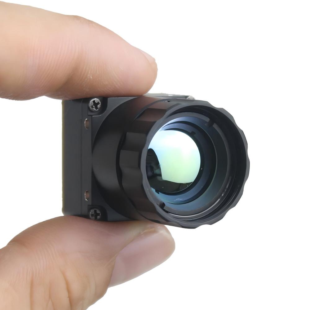
| Physical Dimensions | Ultra-compact micro-footprint | Mini-Size of 21 mm × 21 mm |
| Focal Length Options | Integrated Athermalized Optic | 5 / 9 / 13 / 18 / 35 / 50 / 75 / 100 / 150 mm |
| Interface Support | Digital Radiometric Stream Output | USB Digital Output / Modular Interface |
| Environmental Adaptability | Industrial Operating Envelopes | Stable performance, high adaptability |
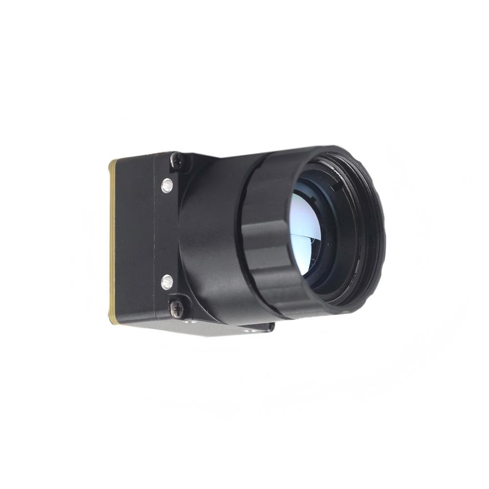
Uncooled LWIR Mini 256*192 Thermal Imaging Camera Module Similar To DJI For Detecting Mines
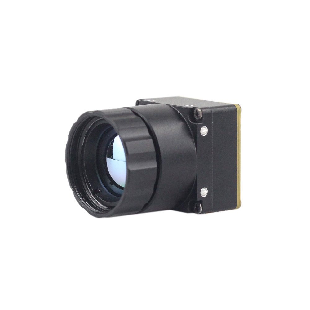
The Mini 256 Uncooled LWIR thermal Camera Module adopts high-performance infrared detectors for ultra-clear thermal imaging and accurate temperature measurement. It captures infrared radiation and outputs a uniform thermal image with full radiometry. Engineered to deliver stable, high-reliability performance within hyper-SWaP-constrained physical envelopes, this core module is exceptionally well suited for integration into micro-drone gimbals, wearable robotic vision nodes, electrical cabinet thermal monitoring, and sub-surface anomaly identification such as humanitarian mine detection operations.
Featuring a 256 × 192 pixel active array on a tight 12 µm pitch, this module balances low thermal noise with minimal compute overhead, making it straightforward to parse on resource-constrained embedded microcontrollers and micro-single-board computers.
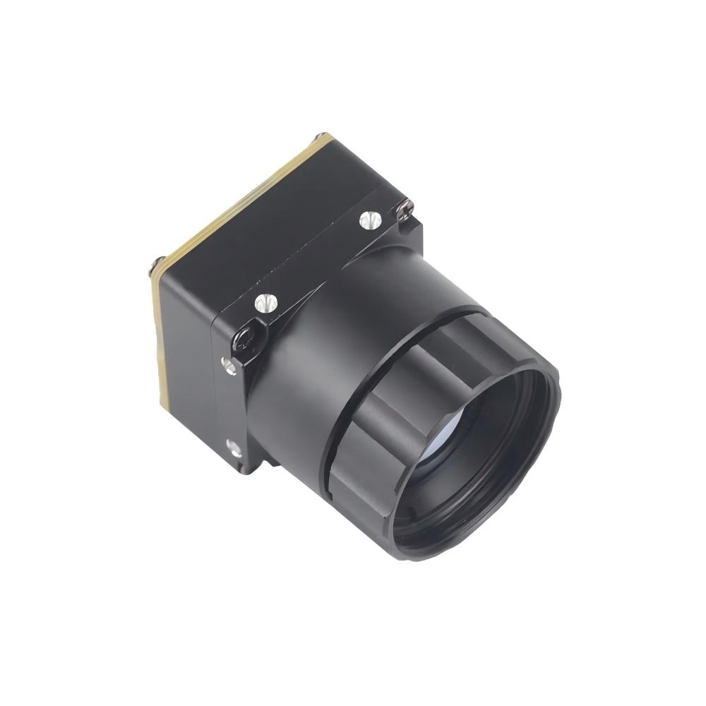
Uncooled LWIR USB Mini 640*512 Thermal Imaging Camera Core Module For Drones Similar To DJI
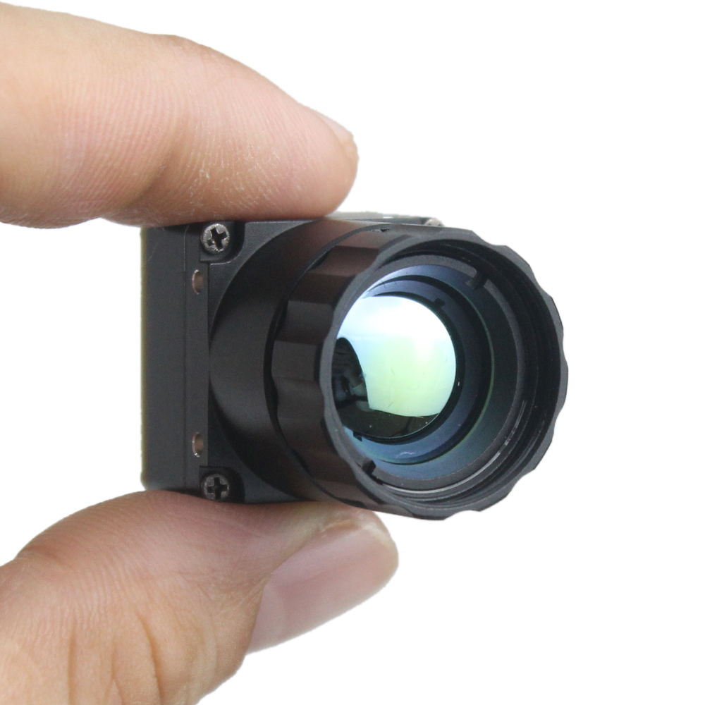
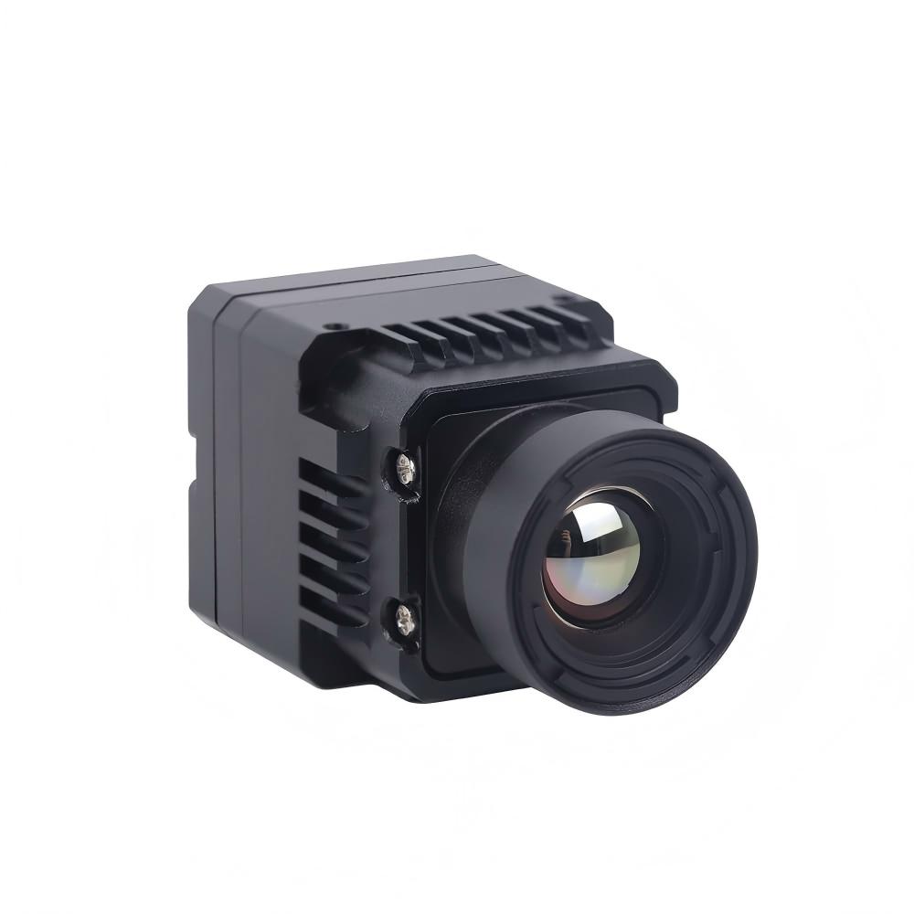
The Mini uncooled infrared thermal imaging module features sharp and crisp image presentation, compact size, and low cost. Measuring an ultra-miniature 21 mm × 21 mm, this high-resolution core module offers native 640 × 512 resolution (with 640 × 480 optional), stable performance, and strong environmental adaptability.
The module provides comprehensive optical flexibility, supporting an extensive array of precision lens configurations including 5 mm, 9 mm, 13 mm, 18 mm, 35 mm, 50 mm, 75 mm, 100 mm, and 150 mm focal lengths. This broad optical support allows systems engineers to tailor the Field of View across a wide range of operational profiles, from broad panoramic perimeter surveillance to extreme stand-off aerial infrastructure inspection. With its direct USB interface, the Mini 640 module integrates smoothly with host computing architectures, streaming high-definition radiometric video directly into mission-critical computer vision and deep learning pipelines.
6. Industrial Thermal Imaging Engineering FAQ
Are budget thermal imaging cameras under $400 actually worth it for PCB and HVAC diagnostics?
When troubleshooting high-density printed circuit boards (PCBs), surface-mount components (such as 0402 or 0201 packages) measure less than a millimeter in physical size. A low-resolution sensor yields an excessively large Instantaneous Field of View (IFOV). Rather than isolating an individual decoupling capacitor undergoing dielectric breakdown, the sensor averages the thermal energy of the failing component across adjacent ground planes and inactive circuit traces, masking the root cause of the fault.
Similarly, in HVAC and building diagnostic workflows, critical building envelope failures (such as missing batt insulation, trapped moisture, or concealed HVAC duct leakage) often exhibit minute temperature deltas of less than 0.5°C to 1.0°C. An imager with an NETD above 70 mK drowns these subtle signatures in background spatial noise. Reliable, repeatable industrial fault analysis requires a minimum sensor resolution of 256 × 192, with 640 × 512 strongly recommended for fine electronics, coupled with a sub-50 mK NETD rating and calibrated radiometric temperature reporting.
Why should I choose an uncooled LWIR thermal core module over an off-the-shelf handheld camera?
A handheld unit typically weighs anywhere from 400 to 1000 grams and draws significant power. Furthermore, handheld cameras operate within closed firmware architectures: they compress radiometric sensor feeds into 8-bit visual video (such as H.264 or MP4) or flattened JPEGs with hard-coded color palettes. This compression discards the raw 14-bit or 16-bit radiometric array data, preventing automated host computers from calculating exact temperatures across individual pixel coordinates.
In contrast, modular OEM uncooled LWIR cores—such as the Mini 640 module—feature an ultra-compact footprint measuring just 21 mm × 21 mm, consume very little power (typically 1.0W to 1.5W), and strip away extraneous mass. They interface directly with host computing platforms via native digital protocols like USB, MIPI-CSI, and parallel CMOS, streaming raw radiometric frames directly into edge processing units like NVIDIA Jetson. This gives embedded automation software direct access to uncompressed temperature matrices, enabling programmatic anomaly detection, closed-loop machine control, and real-time deep learning inference.
Why do cheaper thermal imagers suffer from blurry visuals and frame stutter?
First, international export control regulations (such as the Wassenaar Arrangement) limit consumer thermal imaging cameras to a refresh rate below 9 Hz (typically 8.6 Hz to 8.8 Hz) to prevent low-cost commercial sensors from being repurposed in tactical weapon systems. An imager refreshing at less than 9 frames per second exhibits jarring visual stutter when panned, inducing motion sickness in human operators and causing severe tracking blur on moving robotic platforms.
Second, lower-cost thermal detectors often utilize Amorphous Silicon (a-Si) microbolometer membranes, which exhibit relatively large thermal time constants (τ = 14 ms to 20 ms). Because the physical microbolometer membrane requires significant time to absorb and dissipate heat as the scene changes, fast target movements leave persistent ghosting trails across the focal plane.
Third, entry-level imagers often omit an electromechanical shutter mechanism to reduce production costs. Without a shutter for periodic Flat-Field Correction (FFC), the camera cannot normalize non-uniform thermal drift across the FPA as internal electronics heat up, leading to spatial noise, vertical striping, and visual softening. Industrial-grade VOx thermal modules overcome these problems by utilizing fast-response VOx detectors (τ = 8 ms to 12 ms), high refresh rates of 25 Hz to 50 Hz, mechanical shutter-based FFC calibration, and multi-stage 3D noise reduction filtering.
📚 References & Further Reading
- Industry Standard: Jinde Precision Infrared Optics Manufacturing
- Industry Standard: NVIDIA Jetson Embedded Computing & Edge AI Platforms
- Related Guide: Comprehensive Engineering Guide: Integrating Thermal Camera Core Modules
- Related Guide: High-Resolution Thermal Camera Modules for Aerial and Drone Payloads
- Related Guide: Handbook on Micro-Module Thermal Integration & Embedded Hardware