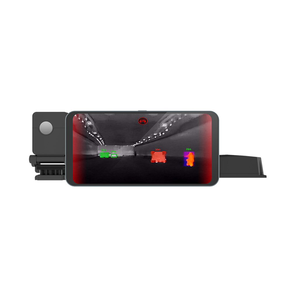


Thermal Cameras Explained: How They Work, Core Tech, and What's Actually Worth Buying
2026年10月20日
Handheld Thermal Camera Guide: Sensor Specs, Field Performance & Pro Selection
2026年10月21日
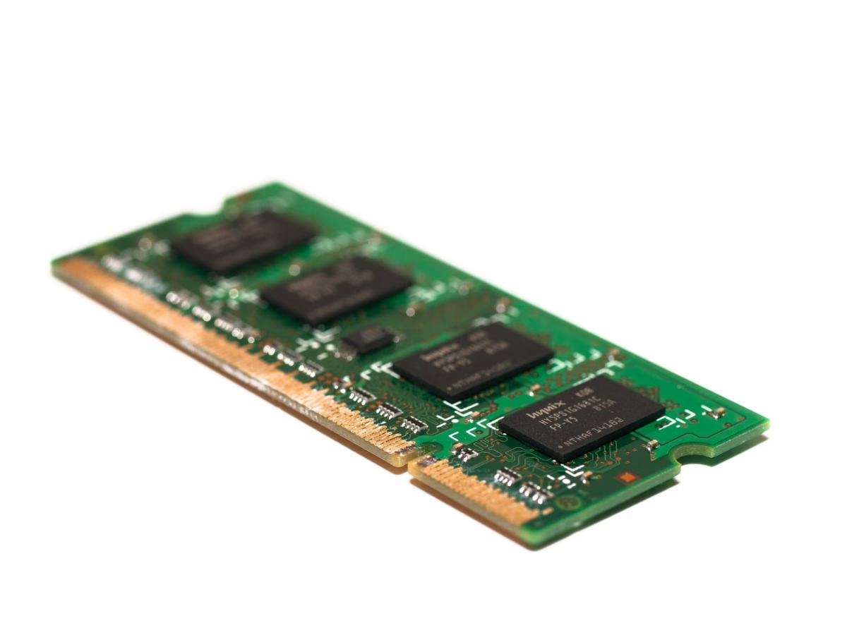
In modern optoelectronics and automated condition monitoring, legacy visual-spectrum sensors face steep physical limitations. Traditional charge-coupled device (CCD) and complementary metal-oxide-semiconductor (CMOS) sensors rely entirely on reflected ambient or artificial photons across the visible spectrum (0.38 to 0.75 μm). In sub-optimal operating environments—such as zero-lux industrial facilities, petrochemical complexes shrouded in volatile aerosols, or aerial search operations obstructed by dense smoke—visual cameras fail completely. For decades, automation engineers attempted to mitigate these blind spots using high-intensity illumination arrays or low-light CMOS sensors. However, these systems still struggle with heavy airborne particulates, weather attenuation, and high-contrast shadows. Furthermore, basic visual imagery cannot quantify the underlying thermodynamic state of target equipment, leaving critical predictive maintenance workflows vulnerable to unmonitored thermal stress and sudden component failure.
Implementing an uncooled infrared thermal camera solves these physical constraints by transitioning from reflected light imaging to passive radiometric emission capture. Operating within the Long-Wave Infrared (LWIR) spectrum (8 to 14 μm), modern uncooled microbolometer focal plane arrays (FPAs) detect the microscopic electromagnetic flux emitted by every object above absolute zero. For original equipment manufacturers (OEMs), robotics designers, and automation engineers, deploying an industrial LWIR core delivers true 24/7 vision independent of environmental lighting, alongside non-contact per-pixel temperature telemetry. By analyzing the engineering trade-offs of microbolometer chemistry, optical material transmission, distance-to-spot metrics, and digital interface protocols, this technical blueprint provides an empirical framework for selecting, calibrating, and embedding high-resolution thermal imaging modules into mission-critical hardware ecosystems.
Table of Contents
- 👉 1. Fundamentals: Atmospheric Windows & LWIR Radiometry
- 👉 2. Sensor Core Architecture: VOx vs. a-Si Microbolometers
- 👉 3. Native Resolution, Pixel Pitch & The Optical D:S Ratio
- 👉 4. Industrial LWIR Modules: Comparative Hardware Breakdown
- 👉 5. Embedded OEM Integration: MIPI, USB & Radiometric Calibration
- 👉 6. Operational Selection Matrix: UAV, Security & Machine Vision
- 👉 7. Comprehensive Industrial Engineering FAQ
1. Fundamentals: Atmospheric Windows & LWIR Radiometry
Every non-contact thermal measurement system relies on the physical laws governing electromagnetic blackbody radiation. Max Planck's radiation law describes the spectral radiance ($L_\lambda$) emitted by an idealized blackbody at thermodynamic temperature $T$ across specific wavelengths ($\lambda$):
L(λ, T) = (2hc2 / λ5) × [1 / (exp(hc / λkBT) - 1)]
Where $h$ represents the Planck constant ($6.626 \times 10^{-34} \text{ J}\cdot\text{s}$), $c$ is the speed of light in vacuum ($2.998 \times 10^8 \text{ m/s}$), and $k_B$ denotes the Boltzmann constant ($1.381 \times 10^{-23} \text{ J/K}$). Integrating Planck's distribution across all wavelengths yields the Stefan-Boltzmann law, establishing that total radiant exitance ($j^*$) scales with the fourth power of absolute temperature:
j* = ε σ T4
Here, emissivity ($\varepsilon$) represents the ratio of thermal radiation emitted by a real surface relative to a theoretical blackbody radiator ($\varepsilon = 1.0$), while $\sigma$ is the Stefan-Boltzmann constant ($\approx 5.670 \times 10^{-8} \text{ W}\cdot\text{m}^{-2}\cdot\text{K}^{-4}$). Industrial materials vary widely in emissivity: heavily oxidized steel surfaces exhibit values between 0.75 and 0.85, whereas polished non-ferrous metals like copper or aluminum drop below 0.05, functioning as thermal reflectors. An uncooled infrared thermal camera translates this incoming radiant energy into measurable electrical impedance changes, generating quantitative thermal profiles without an external excitation beam.
When implementing these thermal systems outside laboratory vacuums, atmospheric transmission windows heavily influence optical throughput. Earth's atmosphere contains gaseous compounds—predominantly water vapor ($H_2O$), carbon dioxide ($CO_2$), and ozone ($O_3$)—that absorb electromagnetic radiation across continuous infrared bands. Optoelectronic hardware is engineered around three primary transmission bands:
- ⚙️ Short-Wave Infrared (SWIR, 0.9 to 1.7 μm): Dominated by reflected solar or active illuminator energy. SWIR behaves similarly to visible spectrum light, relying on glass optics and InGaAs (Indium Gallium Arsenide) sensors. It excels at semiconductor wafer inspection, moisture profiling, and penetrating atmospheric haze, but it cannot measure passive ambient temperatures below 150°C.
- ⚙️ Mid-Wave Infrared (MWIR, 3.0 to 5.0 μm): Captures thermal signatures from hot objects (300°C to 1000°C) and serves specialized optical gas imaging applications (such as volatile organic compound and methane plume visualization). However, MWIR architectures typically require cryogenic Stirling coolers operating at 77 Kelvin. These mechanical coolers introduce severe SWaP-C penalties (Size, Weight, Power, and Cost) and have limited operational lifespans (MTBF ≤ 8,000–15,000 hours).
- ⚙️ Long-Wave Infrared (LWIR, 8.0 to 14.0 μm): Aligns with the peak spectral emission of objects between -40°C and +85°C, as determined by Wien's displacement law ($\lambda_{max} = 2898 / T$). Crucially, this waveband corresponds to an atmospheric transmission window where absorption by $CO_2$ and liquid water reaches a local minimum, making uncooled LWIR thermal cameras the industry standard for environmental monitoring, industrial predictive maintenance, and autonomous navigation.
Standard optical glass (such as Borosilicate or BK7) is completely opaque to LWIR photons above 2.5 μm because of strong lattice absorption bands. As a result, thermal camera lenses require exotic infrared optical materials. Monocrystalline Germanium ($Ge$) provides exceptional optical performance, featuring a high refractive index ($n \approx 4.0$) that enables compact, high-speed lens designs ($f/1.0$). However, Germanium is vulnerable to thermal runaway; its free electron absorption escalates rapidly, causing internal transmission to drop precipitously above 60°C. To combat this limitation in outdoor environments, manufacturers integrate chalcogenide glass compounds (such as $Ge_{33}As_{12}Se_{55}$ or $Ge_{28}Sb_{12}Se_{60}$). Specialized optical providers like LightPath Technologies precision-mold chalcogenide optics with balanced thermo-optic coefficients ($dn/dT$) combined with specialized housing materials. This produces passively athermalized optical assemblies that maintain sharp focal alignment across extreme environmental swings (-40°C to +80°C) without requiring motorized focus compensation hardware.
2. Sensor Core Architecture: VOx vs. a-Si Microbolometers
The core sensor element of an uncooled thermal camera is the microbolometer Focal Plane Array (FPA). Rather than relying on cooled photon detectors that generate charge carriers within a semiconductor valence band, a microbolometer functions as an array of microscopic thermal resistors suspended above an integrated circuit.
Each individual detector pixel features a micro-electromechanical (MEMS) bridge architecture. A central absorbing membrane—typically one to two micrometers thick—is suspended over an evacuated silicon Read-Out Integrated Circuit (ROIC) substrate via slender titanium or silicon nitride legs. These micro-isolation legs provide mechanical support alongside high thermal resistance ($R_{th} \approx 10^7 \text{ K/W}$). When incident LWIR radiation strikes the pixel, the absorbing membrane heats up. This temperature shift ($dT$) changes the membrane's electrical resistance. The underlying ROIC measures this resistance shift by applying a short bias pulse and digitizing the resulting voltage drop. Key performance parameters depend entirely on the thin-film material deposited on the MEMS bridge:
| Physical / Electrical Metric | Vanadium Oxide (VOx) | Amorphous Silicon (a-Si) |
|---|---|---|
| Temperature Coefficient of Resistance (TCR) | -2.0% to -3.0% / Kelvin | -1.5% to -2.5% / Kelvin |
| Noise Equivalent Temperature Difference (NETD) | Superior (≤ 30 mK to 40 mK) | Moderate (≥ 40 mK to 50 mK) |
| 1/f (Flicker) Noise Characteristic | Low (Stable continuous signal) | Higher (Demands frequent offset updates) |
| Thermal Time Constant (τ) | 8 ms to 12 ms | 4 ms to 8 ms |
| Fabrication Methodology | Specialized deposition processes | Standard CMOS line compatible |
Vanadium Oxide (VOx) remains the preferred detector material for high-precision industrial thermography. Thanks to its higher Temperature Coefficient of Resistance (TCR), a fractional change in pixel temperature yields a larger, more measurable electrical signal. Combined with low Johnson and $1/f$ noise characteristics, VOx FPAs achieve a Noise Equivalent Temperature Difference (NETD) below 30 mK ($0.03°C$). This level of sensitivity allows the sensor to resolve minute temperature variations between adjacent targets. Amorphous Silicon ($\text{a-Si}$) offers faster thermal time constants and leverages standard CMOS fabrication lines, which lowers production costs. However, its higher intrinsic noise floor limits its effectiveness in mission-critical applications where high spatial and radiometric resolution is required. For an architectural breakdown of industrial sensor selection workflows, refer to the industrial thermal sensor selection guide.
A persistent challenge in microbolometer engineering is sensor drift, caused by the lack of active cryogenic stabilization. As the camera's external chassis, lens barrel, and internal housing warm up during operation, stray internal infrared photons strike the FPA. This background radiation introduces non-uniform offset shifts across the detector array. Thermal imagers mitigate this drift through Non-Uniformity Correction (NUC). In standard mechanical NUC architectures, a physical shutter blade (often blackened aluminum or copper) drops across the optical path for 250 to 500 milliseconds. This gives the sensor a flat-field temperature reference, resetting offset drift registers across all active pixels. In fast-paced industrial environments—such as drone guidance or dynamic robotics—this shutter freeze can interrupt closed-loop control systems. To solve this, advanced high-reliability cores utilize shutterless NUC algorithms. These systems continuously compute spatial-temporal scene statistics and monitor real-time thermistors placed across the optical barrel, keeping the stream clear without interrupting video telemetry.
3. Native Resolution, Pixel Pitch & The Optical D:S Ratio
Thermal resolution is governed by physical detector geometry, not display interpolation. Entry-level consumer instruments frequently pair tiny $80 \times 60$ or $160 \times 120$ microbolometer sensors with edge-extraction software, overlaying visible light outlines onto an upscaled thermal feed. While this provides recognizable contours on a screen, it offers zero radiometric fidelity for small targets. If a critical thermal fault—such as an overheating PCB surface-mount diode or an electrical distribution clamp—does not cover an entire detector pixel, the sensor averages the target's radiant energy with the colder background. This spatial averaging suppresses measured temperature peaks, obscuring early equipment faults.
High-resolution industrial imaging requires true native focal plane arrays. Upgrading from legacy 17 μm pixels to 12 μm pixel pitch architectures delivers significant operational advantages. Reducing pixel pitch cuts the physical silicon area required for a given resolution by roughly 50%. This enables smaller, lighter optical assemblies and lowers system SWaP-C profile. However, this smaller footprint presents optical challenges: because each 12 μm pixel captures less radiant photon flux than a 17 μm pixel, the optical train requires a fast aperture ($f/1.0$ or $f/1.1$) to preserve low NETD sensitivity.
To accurately calculate optical coverage at specific inspection distances, optical engineers evaluate the Instantaneous Field of View (IFOV):
IFOV = Pixel Pitch (p) / Focal Length (f)
IFOV is measured in milliradians (mrad). It defines the spatial angle subtended by a single physical pixel. For accurate quantitative surface temperature measurements (radiometry), a target cannot simply subtend a single IFOV. Optical diffraction, optical manufacturing tolerances, and intra-pixel cross-talk dictate that targets must cover a dedicated cluster of pixels to overcome the sensor's Modulation Transfer Function (MTF) limits. This constraint establishes the Measurement IFOV (M-IFOV), commonly referred to as the Distance-to-Spot (D:S) ratio:
| Metric Parameter | Optical Definition | Engineering Impact on Radiometry |
|---|---|---|
| IFOV (Spatial Resolution) | $p / f$ (radians) | Calculates minimum target size detectable across the scene background. |
| M-IFOV (Radiometric Spot) | $3 \times \text{IFOV}$ to $4 \times \text{IFOV}$ | Minimum physical footprint required to measure temperature within ±2°C accuracy. |
| Johnson: Detection Criterion | 1.5 resolved lines (3 pixels) | Sufficient energy to determine an object is present in the field of view. |
| Johnson: Recognition Criterion | 6 resolved lines (12 pixels) | Sufficient spatial clarity to classify target class (e.g., human vs vehicle). |
| Johnson: Identification Criterion | 12 resolved lines (24 pixels) | Full spatial profiling enabling detailed target identification. |
Consider an industrial integration monitoring a remote valve assembly 50 meters away using an uncooled LWIR sensor. With a 12 μm pixel pitch and a 25mm lens, the calculated IFOV is $12 \times 10^{-6} / 25 \times 10^{-3} = 0.48 \text{ mrad}$. At a range of 50 meters, a single pixel covers a spatial area of:
Spatial Spot Size = 50 × 1000 mm × 0.00048 rad = 24 mm
While a 24 mm component can be detected by a single pixel, reliably measuring its temperature requires meeting the M-IFOV criteria ($3 \times \text{IFOV}$ minimum). The target must measure at least $72 \text{ mm}$ across to avoid spatial averaging with surrounding structures. When inspection requirements call for analyzing smaller points—such as 10 mm electronic traces—the optical system must be matched with higher native pixel counts ($1280 \times 1024$) or longer focal length lenses.
4. Industrial LWIR Modules: Comparative Hardware Breakdown
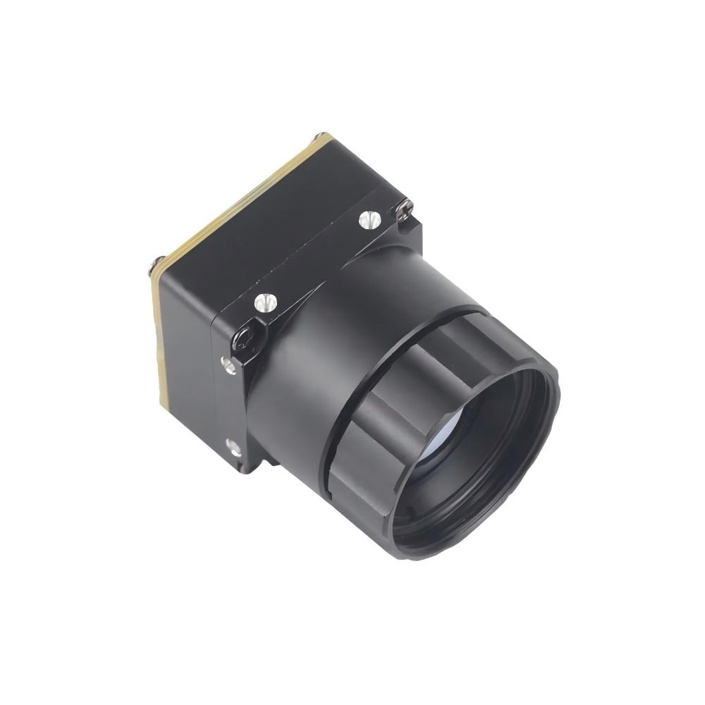
OEM hardware integrators must balance native resolution, power consumption, mechanical volume, and optical speed. The following industrial-grade LWIR camera solutions illustrate distinct engineering approaches across automated factory inspection and mobile unmanned systems.
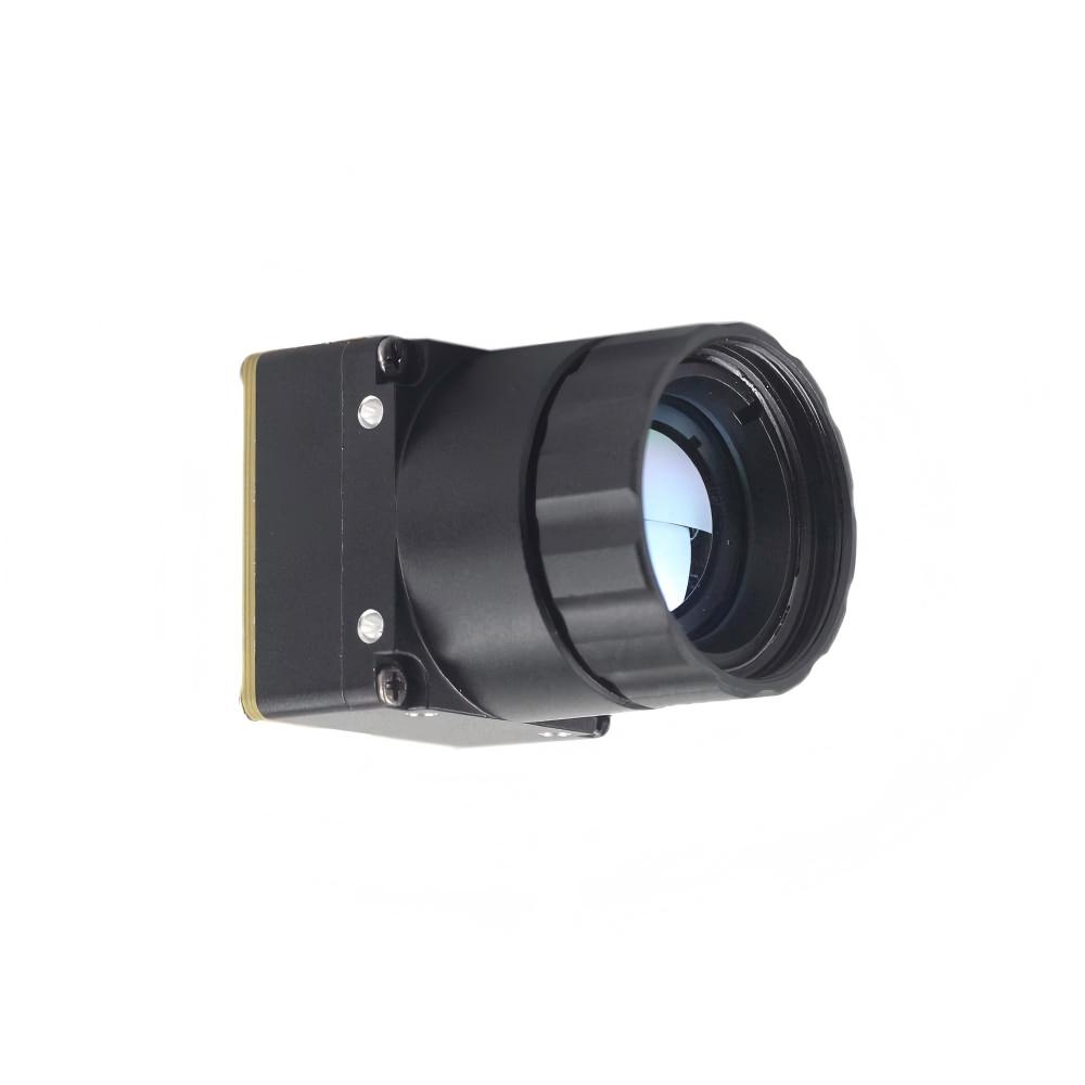
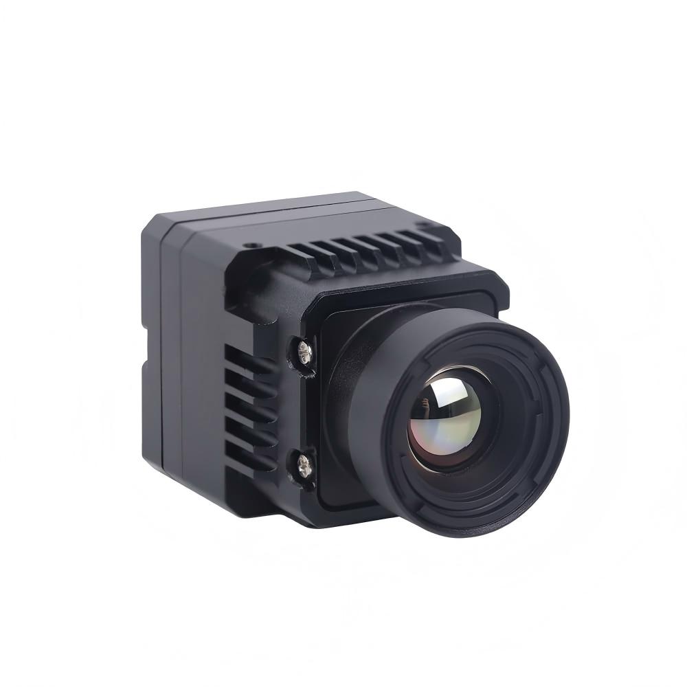
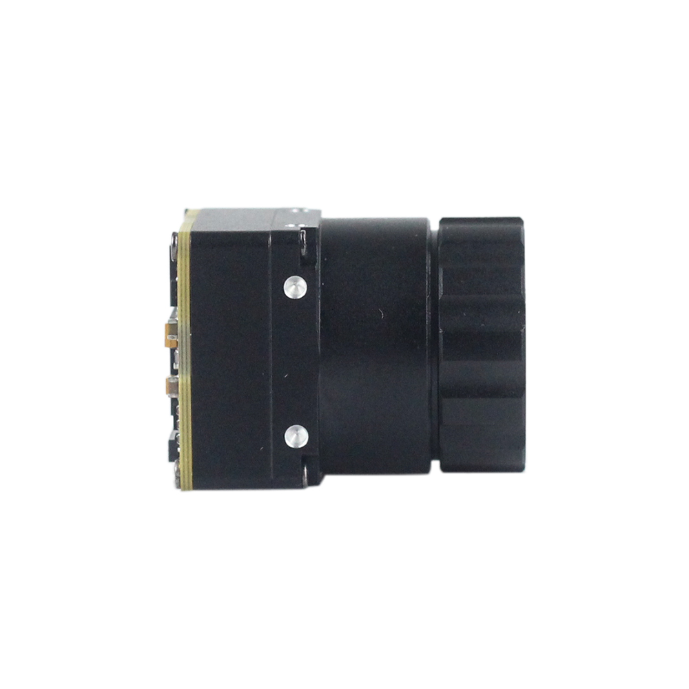
1. High Resolution Uncooled Infrared 1280*1024 Thermal Imaging LWIR Camera
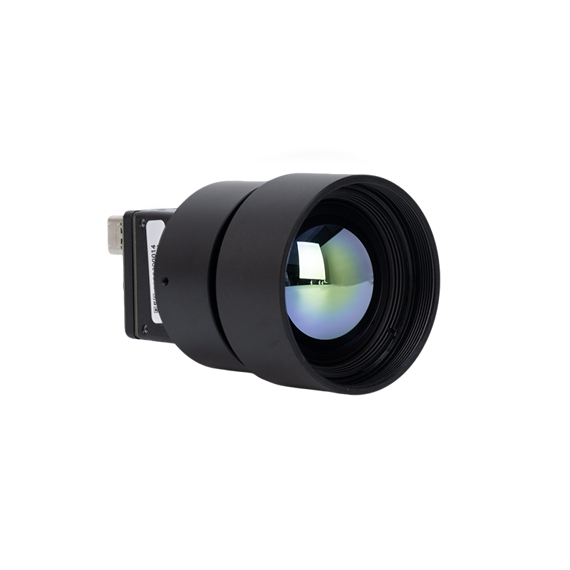
Designed for high-precision metrology, the PRSE5-1280 features a native $1280 \times 1024$ megapixel-class focal plane array. Built around an uncooled VOx microbolometer core, it captures fine thermal details without requiring cryogenic hardware. The unit is paired with an athermalized 25mm lens, balancing a wide field of view with the high angular resolution needed for industrial inspection.
- ⚙️ FPA Architecture: Uncooled Vanadium Oxide (VOx) Microbolometer
- ⚙️ Native Array Matrix: 1280 × 1024 true physical pixels
- ⚙️ Optical Configuration: 25mm Athermalized Precision Lens
- ⚙️ Spectral Waveband: 8 to 14 μm (LWIR)
- ✅ Primary Target Applications: Optical automated inspection (AOI), high-voltage substation monitoring, industrial process control, and perimeter security.
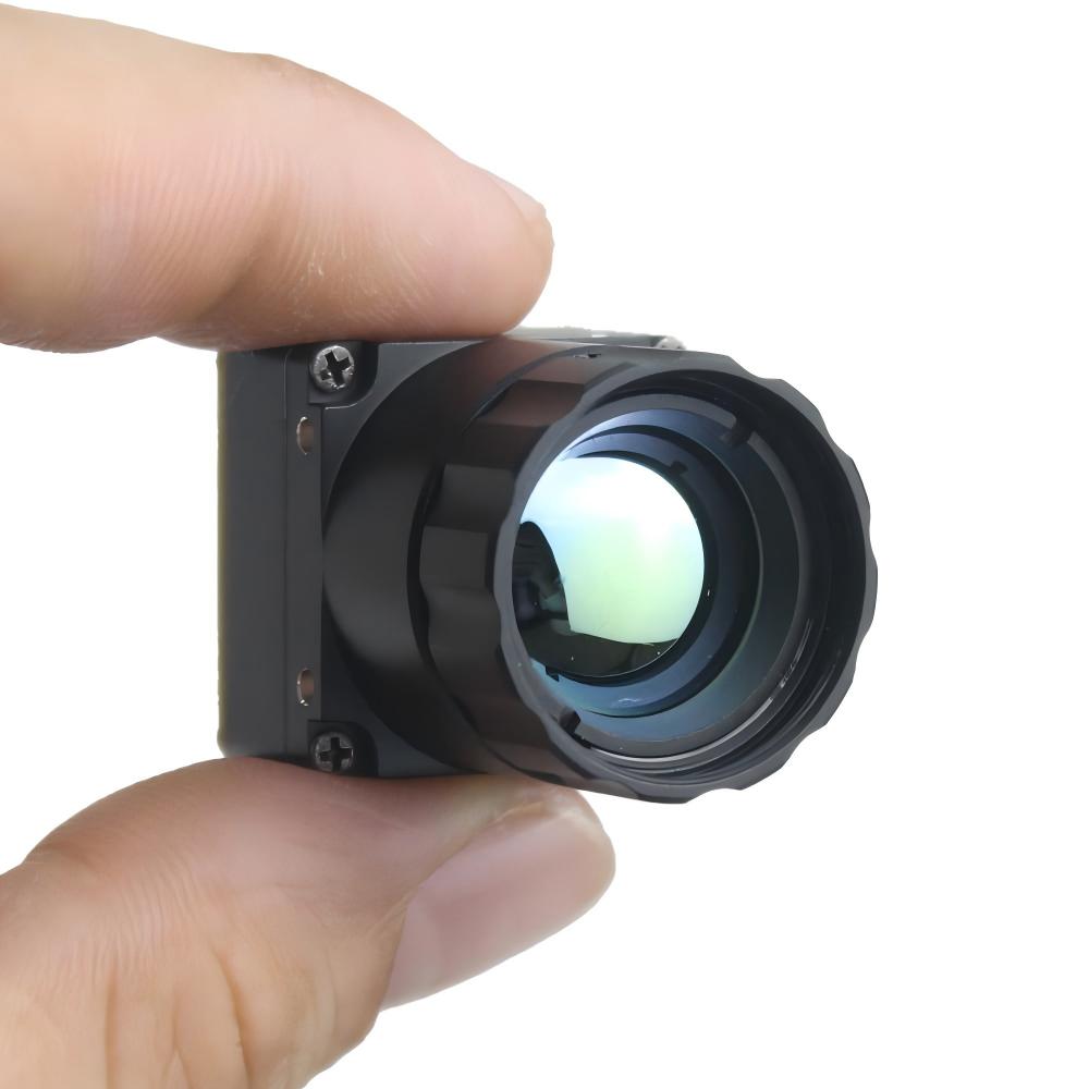
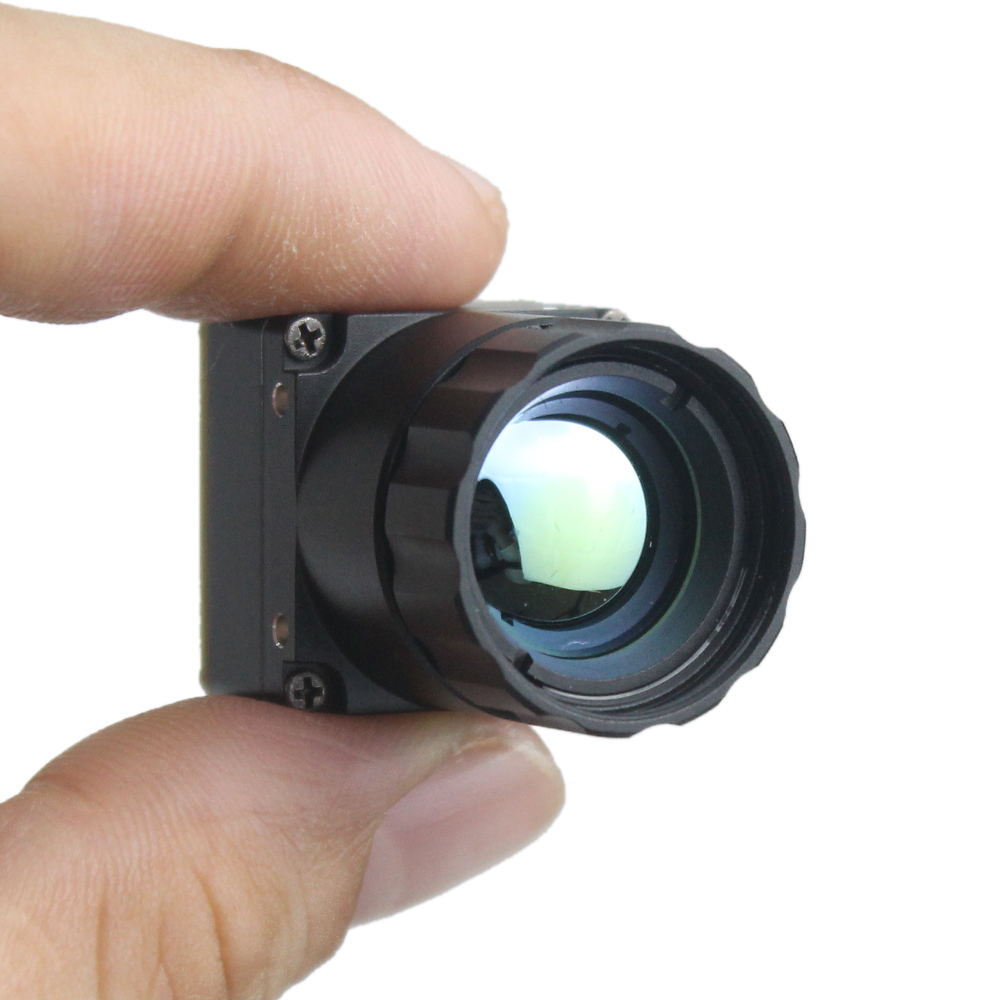
2. Uncooled Infrared MIPI Mini2 640*512 Thermal Camera Module
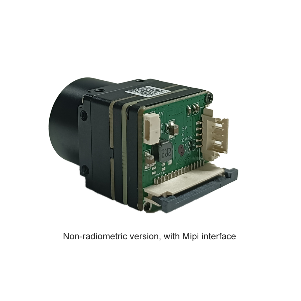
Engineered for weight-sensitive applications, the Mini2 module delivers native $640 \times 512$ resolution in an ultra-compact form factor (with scalable $384 \times 288$ and $256 \times 192$ configurations). Featuring a native MIPI CSI-2 interface, the module streams raw 14-bit data directly into edge processing platforms without the latency of analog decoders or the bulk of industrial USB controllers.
- ⚙️ FPA Architecture: Miniaturized Uncooled Microbolometer Core
- ⚙️ Native Array Options: 640 × 512 (Native), scalable to 384 × 288 or 256 × 192
- ⚙️ Optical Configuration: 9mm Fixed-Focus Wide-Angle Lens
- ⚙️ Electrical Interface: Native Mobile Industry Processor Interface (MIPI CSI-2)
- ✅ Primary Target Applications: Aerial search-and-rescue UAVs, stabilized micro-gimbals, man-portable thermography, and robotics navigation.
| System Metric | PRSE5-1280 Precision Core | Mini2 MIPI Drone Payload Core |
|---|---|---|
| Native Array Resolution | 1280 × 1024 active pixels | 640 × 512 active pixels |
| Optics Assembly | 25mm Athermalized Optic | 9mm Ultra-Compact Optic |
| Pixel Yield (Density) | 1,310,720 discrete measurement points | 327,680 discrete measurement points |
| Sensor Type | Uncooled VOx Microbolometer | Ultra-Lightweight Microbolometer |
| System Interface | Industrial Digital Stream / Radiometric Output | Native Low-Latency MIPI CSI-2 |
| Weight Profile / Envelope | Rugged Industrial Enclosure | Sub-miniature Lightweight Form Factor |
| Primary Deployments | Factory Automation, Electronics AOI, Metrology | Micro Gimbal Assemblies, Drone Payloads, Robotics |
5. Embedded OEM Integration: MIPI, USB & Radiometric Calibration
Integrating an uncooled infrared thermal camera into an embedded system requires careful design across hardware, protocols, and data processing. Unlike standard visual cameras that stream compressed 8-bit YUV or RGB frames, radiometric thermal modules handle raw data representing real temperatures. A typical visual stream compresses color matrices across three 8-bit channels ($2^8 = 256$ dynamic levels per pixel). This standard 8-bit color space cannot capture wide thermal ranges. If a thermal core monitors temperatures from -20°C to +350°C, an 8-bit output limits temperature resolution to roughly 1.45°C per digital level, losing the sub-millikelvin sensitivity of the microbolometer.
To preserve full temperature sensitivity, the camera's ROIC outputs a linear 14-bit or 16-bit digital stream ($2^{14} = 16,384$ discrete dynamic levels). In this raw data format, each digital increment (or Digital Number, DN) typically corresponds directly to temperature—such as 0.01 Kelvin per DN. Transporting this raw data to a processing unit requires matching the hardware interface to the system architecture:
- ⚙️ MIPI CSI-2 (Mobile Industry Processor Interface): The preferred interface for embedded systems, uncrewed aerial vehicles, and mobile edge robotics. MIPI CSI-2 routes high-speed raw differential pixel data straight into an application processor's Image Signal Processor (ISP) or memory space via DMA (Direct Memory Access). By eliminating USB transceiver ICs and bridge conversion layers, MIPI links minimize transmission latency and keep processing overhead low on edge platforms like the NVIDIA Jetson Orin or Raspberry Pi Compute Module 4.
- ⚙️ USB 3.0 / USB3 Vision: Well-suited for factory automation enclosures, fixed test benches, and standard industrial PCs. While USB introduces driver abstraction layers and higher interface latency than MIPI, it simplifies desktop software development and supports direct connectivity via standard UVC (USB Video Class) extensions.
- ⚙️ Analog Video Interfaces (CVBS/PAL/NTSC): While digital interfaces dominate modern automated workflows, analog signaling remains widely used across legacy aerospace systems and low-latency analog FPV video transmitters. For legacy integrations and analog configurations, explore our technical guide on analog thermal camera modules.
Converting a raw 14-bit pixel stream into calibrated temperature data requires applying a multi-stage radiometric calibration pipeline. The host processor must convert the raw Digital Number ($DN$) into true target temperature ($T_{obj}$) using calibrated factory coefficients:
DNlinear = R × [ε τatm L(Tobj) + (1 - ε) τatm L(Trefl) + (1 - τatm) L(Tatm)] + Offset
Where:
- ⚙️ $R$ is the system's radiometric responsivity coefficient established during optical bench blackbody calibration.
- ⚙️ $\tau_{atm}$ represents the atmospheric transmission factor calculated over the inspection distance.
- ⚙️ $T_{refl}$ is the reflected ambient background temperature (critical for low-emissivity targets).
- ⚙️ $T_{atm}$ represents the ambient temperature of the air between the camera and the target.
Thermal system designers must also manage the heat generated within the camera enclosure itself. Industrial enclosures, motorized gimbals, and sealed IP67 housings create internal heat pockets. As the internal lens housing and camera chassis warm up, they emit stray infrared radiation back onto the detector array. Without thermal isolation, this stray energy introduces measurement drift. Reliable OEM designs incorporate mechanical heat sinks directly into the chassis and place precision thermistors along the optical path to monitor internal temperatures in real time. Dynamic calibration tables inside the firmware use these thermistor readings to continuously correct temperature drift, ensuring stable, accurate measurements across changing ambient conditions.
6. Operational Selection Matrix: UAV, Security & Machine Vision
Selecting the optimal infrared thermal camera requires balancing spatial resolution, optical design, thermal sensitivity, and SWaP-C profile. The optimal configuration depends directly on the mechanical, environmental, and computational constraints of each deployment scenario:
| Deployment Scenario | Key Engineering Constraints | Recommended Hardware Profile |
|---|---|---|
| Unmanned Aerial Vehicles (UAVs) & Robotics | Weight limits, battery draw, aerodynamic drag, high-vibration gimbals. | Ultra-compact modules like the Mini2 640×512 with wide 9mm optics, native MIPI CSI-2, and sub-miniature form factor. |
| Automated Quality Control & Electronics Inspection | Small target sizes, tight thermal tolerances (±1°C), stationary automated test setups. | High-resolution cores like the PRSE5 1280×1024 with 25mm optics, high NETD sensitivity (≤35 mK), and raw 14-bit data streaming. |
| Perimeter Security & Infrastructure Monitoring | Long detection ranges (1 km+), wide operational temperature range (-40°C to +60°C), continuous 24/7 uptime. | Athermalized optics (25mm to 50mm lenses), ruggedized IP67 housings, and automated mechanical or shutterless NUC calibration. |
In UAV payloads, system weight dictates operational flight time. Adding an oversized thermal camera payload reduces flight endurance, limits gimbal stabilization margins, and strains drone motors. For aerial search-and-rescue (SAR) or agricultural inspection, the combination of a lightweight footprint, wide field-of-view 9mm lens, and a 640×512 native sensor provides the optimal balance of spatial coverage and flight efficiency. The wide FOV allows operators to survey large areas during high-speed passes, while the native 640×512 resolution preserves thermal sensitivity for spotting anomalies on the ground.
Conversely, automated factory production lines prioritize spatial measurement resolution over system weight. Inspecting packed printed circuit board (PCB) assemblies requires detecting thermal faults on individual components—such as micro-resistors, multi-layer ceramic capacitors, or ball grid array (BGA) packages measuring less than 1 mm across. In these test environments, lower-resolution sensors suffer from spatial averaging across adjacent components, leading to inaccurate temperature readings. Deploying a native 1280×1024 VOx matrix provides the high pixel density needed to resolve individual micro-components, capture sharp edge boundaries, and isolate thermal faults with absolute radiometric precision. For a visual evaluation of real-world thermal camera performance across continuous deployments, watch our thermal camera continuous performance video.
7. Comprehensive Industrial Engineering FAQ
What is the operational difference between an infrared (NIR) camera and an infrared thermal camera?
In contrast, an infrared thermal camera operates in the Long-Wave Infrared (LWIR) band between 8 and 14 μm. At these wavelengths, the camera detects the passive electromagnetic flux emitted by the target itself, as dictated by Planck's law and the Stefan-Boltzmann relationship. It operates without external light sources, cuts through obscuring particulates like dust and smoke, and provides non-contact surface temperature measurements across every individual pixel in the array.
Why are low-cost $200–$400 thermal cameras insufficient for industrial and robotic integration?
Consumer-grade devices also compromise on thermal sensitivity, with NETD ratings often worse than 70 to 100 mK, and rely on export-restricted 9 Hz frame rates that cause severe motion blur in dynamic automation. Industrial LWIR modules deliver native resolutions from 640×512 up to 1280×1024 pixels, fast 25Hz to 50Hz frame rates, high thermal sensitivity (NETD ≤ 30–40 mK), and raw 14-bit radiometric digital streams. This native performance provides the measurement accuracy and consistency needed for automated machine vision pipelines.
How do weather phenomena like rain, fog, and snow impact LWIR measurement accuracy?
To counter atmospheric transmission loss, industrial thermal imaging platforms apply real-time compensation equations. By integrating live relative humidity, ambient temperature, and target distance data, the processing unit recalibrates the radiometric equation to correct for path attenuation. While ambient cooling from rain or snow cannot be entirely eliminated through software, high-sensitivity microbolometers (NETD ≤ 35 mK) can still detect the tiny thermal differentials created by internal heat sources. This sensitivity allows automated systems to spot emerging equipment faults even under challenging environmental conditions.
📚 References & Further Reading
- 🔍 Industry Standard: Specialized Precision Optics & Chalcogenide Materials — LightPath Technologies
- 🔍 Theoretical Physics: Operational Physics and Microbolometer Sensor Architecture — Wikipedia Microbolometer
- 🔍 Related Guide: Industrial Thermal Sensor Core Evaluation & Selection Matrix — دليل اختيار المستشعر الحراري الصناعي
- 🔍 Related Guide: Analog Thermal Camera Integration Architecture & Modules — وحدات الكاميرا الحرارية التناظرية
- 🔍 Application Analysis: Real-World Operational Video Analysis of Thermal Cameras — Реальное видео с тепловизионной камеры