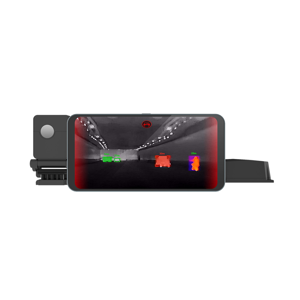

Moduł kamery termowizyjnej — zamówienie hurtowe: rdzenie OEM LWIR do dronów i systemów wbudowanych
10 września 2026
Przewodnik po cenach modułów kamer termowizyjnych: czynniki kosztowe, specyfikacje i sourcing OEM
Poruszanie się po komercyjnym i inżynieryjnym krajobrazie termowizji wymaga zrównoważenia surowej fizyki optycznej z rygorystycznymi ograniczeniami listy materiałowej (BOM). Dla architektów systemów, inżynierów obronnych i integratorów systemów wizyjnych wbudowanych odkrycie niechłodzonego czujnika długofalowej podczerwieni (LWIR) wycenionego na $180 obok innego o pozornie identycznych wymiarach, którego cena wynosi $2 500, powoduje natychmiastowe tarcia zakupowe. Ta skrajna rozbieżność w cenie modułu kamery termowizyjnej nie jest kwestią standardowej marży dystrybutora; odzwierciedla fundamentalne różnice w produkcji matryc ogniskowych (FPA), wydajności pakowania na poziomie wafla (WLP), fizyce transmisji optycznej rzadkich chalkogenków w porównaniu z monokrystalicznym germanem, licencjonowaniu eksportowym liczby klatek na sekundę oraz fabrycznej kalibracji radiometrycznej na poziomie pojedynczego piksela.
W miarę jak produkcja mikrobolometrów przechodzi od starszych metalowo uszczelnianych obudów ceramicznych do przetwarzania na poziomie wafla 12 μm i 8 μm, ekonomika jednostkowa rdzeni wizyjnych LWIR zmienia się gwałtownie. Niezależnie od tego, czy wdrażasz autonomiczne bezzałogowe statki powietrzne (UAV) do inspekcji linii wysokiego napięcia, integrujesz termowizyjne widzenie maszynowe w zautomatyzowanych liniach produkcyjnych, czy projektujesz ręczne termograficzne narzędzia diagnostyczne, wybór odpowiedniego rdzenia czujnika wymaga szczegółowego zrozumienia, w jaki sposób kompromisy między rozmiarem, wagą, mocą i kosztem (SWaP-C) dyktują ceny rynkowe. Poniższy plan rozkłada na czynniki pierwsze dokładne architektury mikrobolometrów, elementy optyczne, protokoły danych i poziomy produkcji, które regulują harmonogramy cen OEM na całym świecie.
Spis treści
- 👉 Kluczowe czynniki kosztowe: matryce ogniskowe (FPA) i pakowanie na poziomie wafla
- 👉 Optyka podczerwona: monokrystaliczny german a formowane szkło chalkogenkowe
- 👉 Kalibracja radiometryczna, czułość NETD i dokładność termiczna
- 👉 Wbudowane protokoły interfejsów: MIPI-CSI, USB-C i obliczenia brzegowe AI
- 👉 Liczba klatek na sekundę, zgodność eksportowa (ITAR/EAR) i sourcing międzynarodowy
- 👉 Benchmarki komercyjne: specyfikacje modułów kamer termowizyjnych OEM i tabela cen
- 👉 Całkowity koszt posiadania (TCO) i optymalizacja BOM dla integratorów systemów
- 👉 Szczegółowe techniczne FAQ
- 👉 Protokół RFQ i sourcingu dla integratorów systemów
Kluczowe czynniki kosztowe: matryce ogniskowe (FPA) i pakowanie na poziomie wafla
Głównym wyznacznikiem ceny każdego modułu kamery termowizyjnej jest niechłodzona mikrobolometryczna matryca ogniskowa (FPA). W przeciwieństwie do czujników obrazu światła widzialnego (CMOS i CCD), które opierają się na krzemowych fototranzystorach wykrywających fale elektromagnetyczne w zakresie od 0,4 μm do 0,7 μm, mikrobolometry LWIR muszą absorbować promieniowanie cieplne w całym spektrum od 8 μm do 14 μm. Wymaga to fundamentalnie odmiennej inżynierii materiałowej, mikroobróbki MEMS (systemów mikroelektromechanicznych) oraz technik hermetyzacji próżniowej, które wprowadzają poważne wyzwania związane z wydajnością krzemu.
Mikrobolometr nie przekształca fotonów bezpośrednio w pary elektron-dziura. Zamiast tego każdy pojedynczy piksel składa się z mikroskopijnej zawieszonej struktury mostkowej — zwykle wytwarzanej z azotku krzemu — pokrytej cienkowarstwowym materiałem reagującym termicznie. Padające promieniowanie podczerwone nagrzewa mostek, zmieniając jego opór elektryczny. Ta minimalna zmiana oporu jest próbkowana przez znajdujący się pod spodem układ odczytowy (ROIC). Ponieważ cząsteczki gazów atmosferycznych odprowadzałyby ciepło z zawieszonego mostka na drodze konwekcji, niszcząc precyzję pomiaru, cała matryca mikrobolometrów musi być trwale zamknięta w komorze wysokiej próżni.
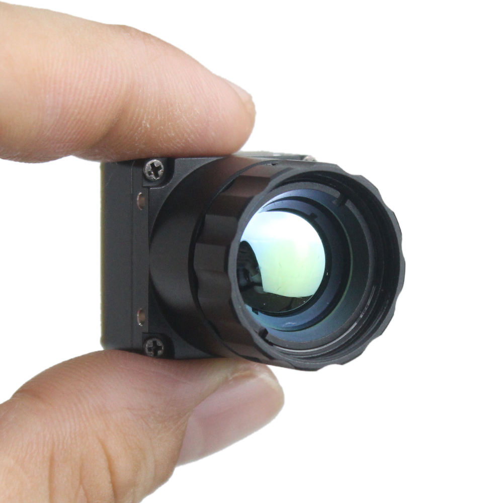
Proces produkcyjny obejmuje złożoną mikromechanikę powierzchniową, w której warstwy ofiarne z poliamidu są wytrawiane za pomocą plazmowych popielarek tlenowych, pozostawiając delikatne mostki zawieszone zaledwie mikrony nad podłożem ROIC. Jeśli naprężenie strukturalne osadzonych cienkich warstw nie zostanie zrównoważone z tolerancją poniżej megapaskala, mikromostki zapadają się, zwijają lub ulegają delaminacji. Ta rzeczywistość ogranicza uzysk surowych płytek krzemowych do poziomów znacznie niższych niż w standardowych komercyjnych liniach produkcji CMOS.
Tlenek wanadu (VOx) kontra amorficzny krzem (a-Si)
Wybór surowego materiału termoczułego zasadniczo determinuje zarówno wydajność modułu, jak i cenę detaliczną:
- ⚙️ Tlenek wanadu (VOx): VOx zapewnia wysoki temperaturowy współczynnik rezystancji (TCR) wynoszący około 2% do 3% na kelwin, w połączeniu z niskim szumem 1/f. Daje to wyższą czułość (niższy NETD) i szybsze stałe czasowe termiczne (zazwyczaj od 8 ms do 12 ms). Jednak przetwarzanie VOx wymaga ściśle kontrolowanego osadzania warstw atomowych (ALD) i reaktywnego trawienia jonowego, co utrzymuje wysokie koszty oprzyrządowania fabrycznego. Jest to dominująca technologia chemiczna dla precyzyjnych modułów inspekcyjnych przemysłowych, wojskowych i profesjonalnych dronów.
- ⚙️ Krzem amorficzny (a-Si): Mikrobolometry a-Si mogą być przetwarzane na konwencjonalnych liniach produkcji półprzewodników przy użyciu standardowego chemicznego osadzania z fazy gazowej wspomaganego plazmą (PECVD). Chociaż obniża to koszty produkcji płytek o 30% do 45%, a-Si ma niższą przewodność elektryczną, wyższy szum własny i niższy TCR (około 1,5% do 2% na kelwin). Aby to skompensować, matryce a-Si często wymagają dłuższych czasów integracji, co skutkuje opóźnieniem termicznym, rozmyciem ruchu i podwyższonymi wartościami NETD (>50 mK), ograniczając je do podstawowej diagnostyki HVAC i konsumenckich mierników punktowych.
Migracja z rastra pikseli 17 μm do 12 μm i 8 μm
Powierzchnia krzemu bezpośrednio determinuje uzysk produkcyjny. Przemysł czujników optycznych stopniowo zmniejszał raster pikseli mikrobolometrów ze starszych standardów 25 μm i 17 μm do węzłów 12 μm i 8 μm:
- ⚙️ Skalowanie uzysku z płytek: Przejście niechłodzonej matrycy FPA 640×512 z rastra 17 μm (aktywny obszar matrycy: ~10,9 mm × 8,7 mm) na raster 12 μm (aktywny obszar matrycy: ~7,68 mm × 6,14 mm) zmniejsza fizyczną powierzchnię struktury o prawie 50%. Standardowa płytka krzemowa 200 mm (8 cali) może zatem wyprodukować ponad dwukrotnie więcej sprawnych struktur, co znacząco obniża jednostkową cenę rdzenia.
- ⚙️ Miniaturyzacja optyki: Mniejsze obudowy czujników wymagają proporcjonalnie mniejszych ogniskowych obiektywów, aby osiągnąć to samo pole widzenia (FOV). Rdzeń 12 μm może wykorzystywać aperturę optyczną o połowę mniejszej objętości fizycznej niż rdzeń 17 μm, generując wtórne oszczędności kosztów w drogich elementach ze szkła germanowego.
- ⚙️ Granice dyfrakcji i izolacja termiczna: Zmniejszanie poniżej 12 μm w kierunku 8 μm zbliża piksele do centralnej długości fali światła LWIR (10 μm). Wprowadza to poważne wyzwania związane z dyfrakcją optyczną, które wymagają ściślejszych tolerancji produkcyjnych w optyce oraz zaawansowanego cyfrowego usuwania rozmycia w układzie ROIC, równoważąc część oszczędności kosztów krzemu.
Ekonomika pakowania na poziomie płytek (WLP)
Historycznie mikrobolometry były zamykane indywidualnie w wysokopróżniowych obudowach ceramicznych lub pozłacanych metalowych ze zintegrowanymi materiałami getterowymi pochłaniającymi cząsteczki odgazowywane w czasie. Takie podejście wymagało kosztownego montażu pick-and-place, ręcznego pompowania próżniowego i hermetycznego zgrzewania szwów, stanowiąc do 60% całego BOM czujnika.
Nowoczesne komercyjne moduły kamer termowizyjnych wykorzystują pakowaniu na poziomie wafla (WLP). W technologii WLP cały wafel mostków MEMS mikrobolometru jest łączony w środowisku ultrawysokiej próżni z górnym waflem krzemowym z wytrawionymi wnękami optycznymi i antyrefleksyjnymi oknami krzemowymi. Poszczególne matryce są następnie wycinane z połączonej kanapki z wstępnie uformowanymi uszczelnieniami próżniowymi. WLP obniża koszty pakowania z setek dolarów za sztukę do kilkudziesięciu dolarów. Jednak początkowy zestaw masek, nakłady inwestycyjne na bonder waflowy oraz inżynieria aktywacji gettera wymagają początkowych nakładów kapitałowych rzędu kilku milionów dolarów. To wyjaśnia, dlaczego tylko garstka globalnych producentów pierwszego poziomu może wycenić moduły WLP 256×192 konkurencyjnie poniżej $200 przy dużych wolumenach.
Aby uzyskać obszerny przegląd koncepcyjny dynamiki czujników termicznych i możliwości noktowizyjnych w trudnych warunkach eksploatacji, zapoznaj się z naszym przewodnikiem inżynieryjnym na temat dynamiki noktowizyjnych kamer termicznych.
Optyka podczerwona: monokrystaliczny german a formowane szkło chalkogenkowe
Kamery światła widzialnego wykorzystują niedrogie formowane wtryskowo soczewki akrylowe lub wysokonakładowe szkło koronowe (BK7), które kosztują mniej niż dolara. Natomiast niechłodzone promieniowanie LWIR (8–14 μm) jest całkowicie blokowane przez standardowe szkło optyczne. Moduły termiczne muszą polegać na specjalistycznych materiałach przepuszczających podczerwień, co sprawia, że zespół optyczny jest jednym z najbardziej zmiennych czynników wpływających na ogólną cenę modułu kamery termicznej.
| Materiał optyczny | Transmisja (8–14 μm) | Współczynnik załamania (n) | Rozszerzalność termiczna (dn/dt) | Względny koszt BOM |
|---|---|---|---|---|
| German monokrystaliczny (Ge) | ~95% (z wielowarstwową powłoką AR) | 4,002 @ 10 μm | Wysoka (3,96 × 10⁻⁴ K⁻¹) | Wysoki ($$$$) |
| Formowane szkło chalkogenkowe (np. BD6, GASIR) | ~65%–72% (bez powłoki), >90% (AR) | 2,4 – 2,8 @ 10 μm | Niska (0,3 – 0,5 × 10⁻⁴ K⁻¹) | Medium ($$) |
| High-Purity Float-Zone Silicon (Si) | ~50%–55% (uncoated) | 3.42 @ 10μm | Moderate (1.5 × 10⁻⁴ K⁻¹) | Low ($) |
German monokrystaliczny (Ge)
Germanium is the premier material for military and precision industrial thermal optics. It possesses an exceptionally high refractive index (n ≈ 4.0), allowing optical designers to build thin, low-curvature lens profiles that minimize optical aberrations even at high numerical apertures (f/1.0 to f/1.2).
However, Germanium creates severe cost bottlenecks. Raw crystalline ingots must be grown via the Czochralski process, diamond-turned on single-point diamond turning (SPDT) CNC lathes, and coated with diamond-like carbon (DLC) or multi-layer anti-reflective (AR) coatings to prevent high Fresnel reflection losses. Furthermore, Germanium exhibits high thermal focal drift (dn/dt = 3.96 × 10⁻⁴ K⁻¹). Without complex athermalization mechanisms (mechanical stepper motors or bi-metallic expanding sleeves), the focus shifts rapidly over environmental operating temperatures (–20°C to +60°C). Incorporating optical or mechanical athermalization adds mechanical complexity and cost to the final module.
Molded Chalcogenide Glass
To slash thermal module production costs for automotive night vision and mini drone deployments, optical manufacturers developed chalcogenide glasses (mixtures of selenium, sulfur, and tellurium). These materials can be heated and stamped using precision tungsten carbide or silicon carbide molds at high volumes. This bypasses the slow, subtractive diamond-turning process required for Germanium, reducing lens production cycle times from hours to minutes.
In addition, chalcogenide has a significantly lower thermo-optic coefficient (dn/dt), enabling purely passive optical athermalization when combined with standard aluminum or plastic lens barrels. The trade-off lies in its lower refractive index (n ≈ 2.5), requiring more lens elements or steeper curvatures to achieve the same light-gathering power (f-number), alongside slightly lower transmission efficiency.
Aperture Sizing (f/1.0 vs. f/1.4)
A lens's f-number indicates its light-gathering capability. In thermal imaging, the thermal flux hitting the detector scales inversely with the square of the f-number:
Radiant Flux (E) ∝ 1 / (f/#)²
An f/1.0 lens delivers twice the thermal radiant flux to the microbolometer compared to an f/1.4 lens. However, achieving an f/1.0 aperture requires a substantially larger optical clear diameter, doubling or tripling the raw mass of Germanium needed. Consequently, compact OEM cores targeted for budget-conscious commercial applications frequently utilize f/1.2 to f/1.4 chalcogenide lenses, relying on aggressive software denoising algorithms to mask the resulting photon deficit.
Kalibracja radiometryczna, czułość NETD i dokładność termiczna
A core divergence that shapes the price spectrum of thermal camera modules is the difference between qualitative imaging cores and radiometric measurement cores. While qualitative cameras display relative heat gradients as pseudo-color imagery, radiometric modules perform absolute temperature measurement at every individual pixel across the focal plane array.
Równoważna szumowi różnica temperatury (NETD)
NETD, quantified in milliKelvins (mK), measures the sensor's sensitivity—the smallest temperature variance the core can discern above its own electronic and thermal noise floor:
- ✅ NETD < 30mK (Grade A Core): Found in precision industrial diagnostic modules, gas leak detectors, and tactical gear. The imagery remains clean, sharp, and artifact-free even in low-contrast conditions, such as dense fog, rain, or overcast nights where all objects reach thermal equilibrium.
- ⚙️ NETD < 50mK (Standard Industrial Grade): Standard for electrical panel monitoring, basic building envelope analysis, and commercial drone payloads.
- ⚠️ NETD > 60mK – 80mK (Low-Cost Grade): Prone to salt-and-pepper noise and temporal patterning unless filtered aggressively, which introduces smearing on moving targets.
The scientific methodology underpinning these radiometric principles is comprehensively cataloged on the Wikipedia Obrazowanie termowizyjne reference.
Non-Uniformity Correction (NUC) and Calibration Overheads
Every microbolometer pixel on a focal plane array has a slightly different gain, offset, and temperature response. To eliminate fixed-pattern noise (FPN), modules employ korekcji niejednorodności (NUC):
- ⚙️ Mechanical Shutter Modules: Incorporate a precision micro-solenoid and an internal paddle that momentarily drops in front of the array to provide an isothermal baseline. The solenoid mechanism, driving circuitry, and calibration add both mechanical failure points and manufacturing expense.
- ⚙️ Shutterless Modules: Use sophisticated real-time scene-based algorithms (Scene-Based Non-Uniformity Correction or SBNUC). While eliminating mechanical hardware, shutterless designs require powerful on-board FPGAs or DSPs to process running spatio-temporal filters, increasing edge computing costs.
Radiometric Factory Calibration Arrays
Radiometric modules do not just stream video; they compute the absolute temperature of an object at every pixel, factoring in target emissivity, reflected apparent temperature, atmospheric distance, and relative humidity. To deliver an accuracy of ±2°C or ±2%, modules must undergo automated temperature environmental chamber testing during manufacturing.
An uncooled module is mounted inside a thermal cycling chamber (typically running across –20°C to +60°C) and calibrated against high-precision NIST-traceable blackbody calibration sources at multiple setpoints. This factory procedure takes hours per unit, tying up expensive environmental chambers and calibration hardware. This "calibration tax" can easily add $150 to $600 to the module's wholesale price, distinguishing a raw observation camera from a metrology instrument.
For broader operational applications of these micro-thermal components in everyday equipment and field tools, explore our article detailing practical commercial thermal imaging applications.
Wbudowane protokoły interfejsów: MIPI-CSI, USB-C i obliczenia brzegowe AI
Modern embedded vision platforms have moved past legacy analog composite video (CVBS/PAL/NTSC). Integrators require high-bandwidth digital data streams to feed neural network inference engines, flight controllers, and industrial PLCs. The communication interface, software development kit (SDK), and on-board processing engine deeply influence the total integration cost.
Digital Interface Hardware Trade-Offs
- ✅ MIPI CSI-2 (Interfejs procesora w urządzeniach mobilnych): The gold standard for drone payloads, handheld imagers, and edge computing boards (such as NVIDIA Jetson Orin and Raspberry Pi Compute Module 4). MIPI delivers low latency, high throughput, and zero protocol-conversion overhead. Thermal modules utilizing native MIPI outputs eliminate the mass, heat, and component cost of USB bridge transceivers, delivering the leanest SWaP-C profile. Hardware houses like Arducam specialize in designing high-throughput MIPI-to-embedded bridges to streamline this data acquisition pipeline.
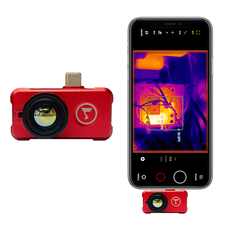
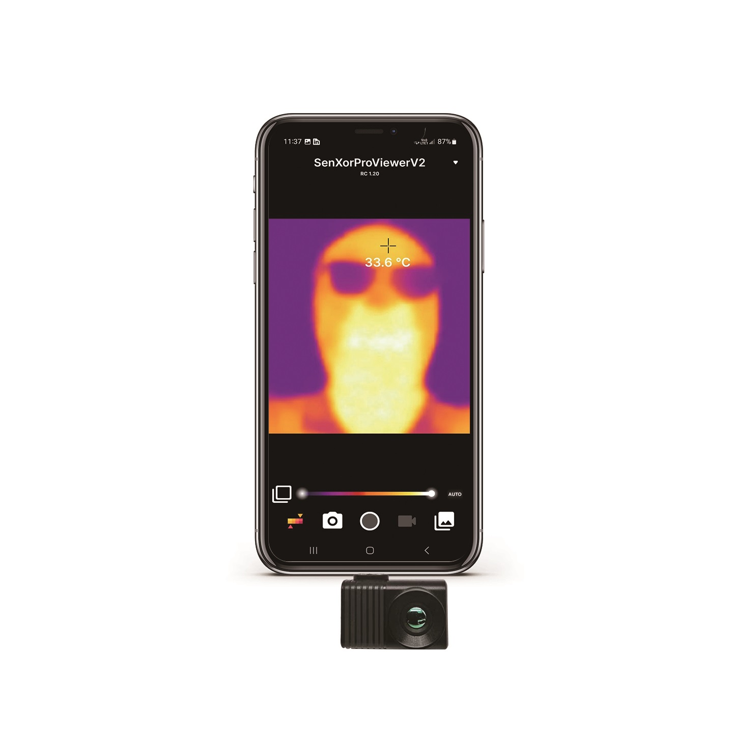
- ⚙️ USB 2.0 / USB-C (UVC + Y16 Radiometric): Commonly deployed for rapid prototyping, secondary inspection tools, and Android smartphone attachments. A standard USB Video Class (UVC) stream supplies an 8-bit colorized pseudo-stream for visual display, while an alternate endpoint delivers a 14-bit or 16-bit raw digital data stream containing raw Kelvin pixel values. USB bridges add $10–$25 to the BOM and consume slightly more operating power (0.2W to 0.5W).
- ⚙️ Parallel DVP / SPI / UART: Utilized by low-cost microcontrollers (e.g., STM32, ESP32) for rudimentary thermal detection, smart home occupancy sensing, and low-speed machinery monitoring. While hardware components are economical, limited bandwidth typically restricts frame rates to ≤ 9Hz with lower spatial resolution.
On-Board ISP & Edge AI Feature Sets
Does the thermal module output raw, uncalibrated detector counts, or does it feature an integrated Image Signal Processor (ISP)?
- ⚙️ Raw Stream Core: Requires the host application CPU/GPU to run compute-intensive dead pixel concealment, non-uniformity correction, spatial noise reduction, and palette mapping. This saves hardware cost on the sensor module itself, but inflates system-level power consumption and host compute requirements.
- ✅ Smart Core with Edge AI: High-end OEM modules embed an integrated FPGA, DSP, or low-power neural processing unit (NPU). These processors run on-board Digital Detail Enhancement (DDE), dynamic range compression, automatic target tracking, and temperature anomaly threshold alarms directly on the sensor core. While this increases the bare module price by 20% to 40%, it reduces host processing loads, allowing systems to operate on lightweight microcontrollers.
To examine how primary industrial thermal engines operate under demanding factory conditions, review our analysis on industrial thermal imaging cores and fire monitoring sensors.
Liczba klatek na sekundę, zgodność eksportowa (ITAR/EAR) i sourcing międzynarodowy
Procurement officers evaluating international thermal camera module pricing often encounter two nearly identical modules—one running at 9Hz and another at 25Hz, 30Hz, or 50Hz—with significant price disparities or divergent supply-chain restrictions. This disparity stems from international arms and dual-use export regulations.
The 9Hz Regulatory Threshold
Under the United States International Traffic in Arms Regulations (ITAR) and the Export Administration Regulations (EAR ECCN 6A003.b.4.b), along with multilateral agreements such as the Wassenaar Arrangement, uncooled thermal imaging cameras capable of capturing at ≥ 9Hz (frames per second) are categorized as dual-use military technologies. The underlying assumption is that high-frame-rate thermal sensors can be integrated into dynamic targeting, anti-air tracking, or guided munitions platforms.
Consequently, manufacturers release "slow-scan" 9Hz capped versions of their sensors for global consumer and low-risk commercial markets. Because these 9Hz cores avoid complex compliance reporting, export licensing fees, end-user verification procedures, and legal liabilities, they are priced substantially lower than their 25Hz, 30Hz, or 50Hz equivalents.
The True Cost of High-Framerate Sourcing
For applications involving high-speed moving targets—such as drone flight gimbals, autonomous vehicle navigation, high-speed rail track inspections, and sports science analysis—a 9Hz sensor creates unacceptable spatial motion blur, stutter, and latency.
When sourcing 25Hz, 30Hz, or 50Hz modules:
- ⚙️ Administrative Overhead: Sourcing non-domestic high-frame-rate modules (such as European or Asian non-ITAR alternatives) requires End-User Certificates (EUC) and import authorizations, extending lead times by 4 to 12 weeks.
- ⚙️ OEM Price Premium: Tier-1 manufacturers apply an administrative and supply-chain markup to high-rate variants, often running 15% to 35% above identical 9Hz core hardware, purely to offset ongoing export compliance, traceability tracking, and legal auditing infrastructures.
Benchmarki komercyjne: specyfikacje modułów kamer termowizyjnych OEM i tabela cen
To help hardware integrators map performance specs to commercial reality, the table below provides an architectural comparison of modern, high-demand uncooled OEM LWIR camera modules. These units represent the current state-of-the-art in compact, SWaP-optimized, high-reliability infrared integration.
| Module Model | Rozdzielczość i rozstaw pikseli | Optics & Focal Length | NETD & Radiometry | Interface & SWaP | Est. OEM Price Tier |
|---|---|---|---|---|---|
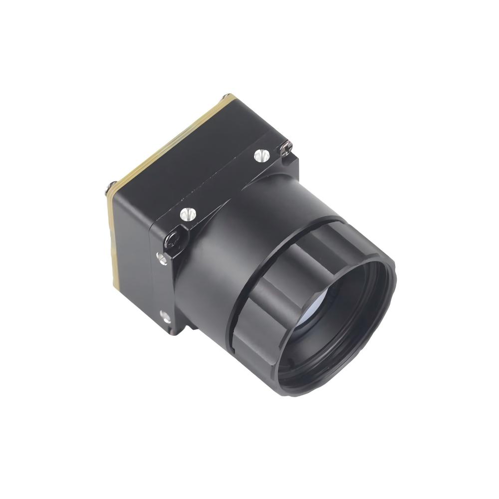
| Niechłodzony moduł dronowy Mini2 640x512 9mm na podczerwień | 640×512 12μm VOx Microbolometer |
9mm Athermalized Lens Wide FOV Mapping |
NETD ≤ 40mK (@25°C) Point, Line, Area Radiometry |
MIPI-CSI / USB / DVP Mass: < 20g | Power: ≤ 0.8W |
Mid-to-High OEM Tier $550 – $950 (Volume Tiered) |
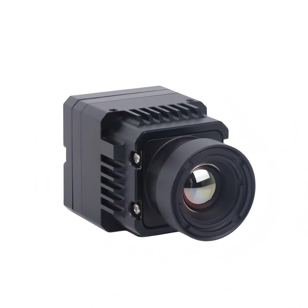
| Mini 256 niechłodzony moduł kamery termowizyjnej LWIR | 256×192 12μm VOx High-Performance |
Compact Fixed Focus Rugged Target Optimized |
NETD ≤ 50mK Uniform Radiometric Output |
USB / UART / Industrial Direct Mass: < 15g | Power: ≤ 0.5W |
Value OEM Entry Tier $160 – $280 (Volume Tiered) |
| Tactical Mil-Spec Core (Legacy Ceramic) | 640×512 17μm Metal Hermetic VOx |
25mm DLC Coated Germanium Single-Point Diamond Turned |
NETD < 25mK Full Metrology Class |
Camera Link / RS-422 Mass: > 120g | Power: > 2.2W |
High Defense Tier $2,200 – $4,500+ (ITAR Restricted) |
Product Deep Dive: Uncooled Infrared Mini2 640 384 256 9mm Thermal Imaging Camera Module For Drones
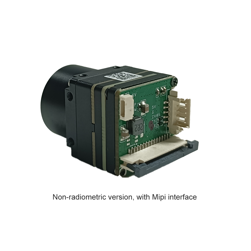
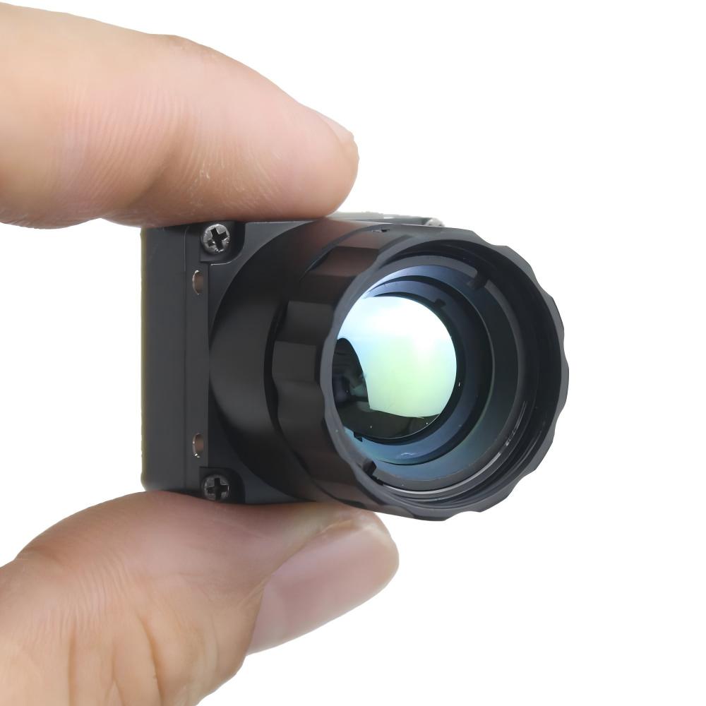
The Uncooled Infrared Mini2 640x512 9mm Thermal Imaging Camera Module is purpose-engineered for high-end drone gimbals, robotic systems, and compact aerial monitoring platforms. Featuring crisp image presentation and low unit cost, it integrates high-resolution 12μm VOx sensor architecture into an ultra-compact footprint.
- ✅ Opcje rozdzielczości: 640×512 (also available in 384×288 and 256×192 configurations)
- ⚙️ Konfiguracja optyczna: 9mm athermalized LWIR lens delivering exceptional broad-field spatial coverage
- ⚙️ Kompatybilność interfejsów: Native MIPI interface directly accessible by embedded flight computers and Linux SoCs
- ✅ SWaP Profile: Sub-20g total weight, minimizing drone payload strain and prolonging airborne flight endurance
Product Deep Dive: Uncooled LWIR Mini 256*192 Thermal Imaging Camera Module Similar To DJI For Detecting Mines
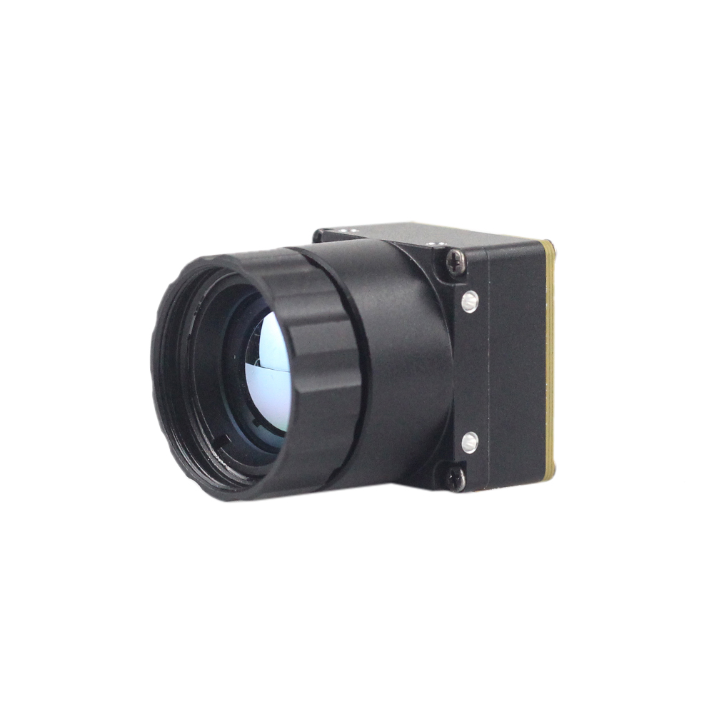
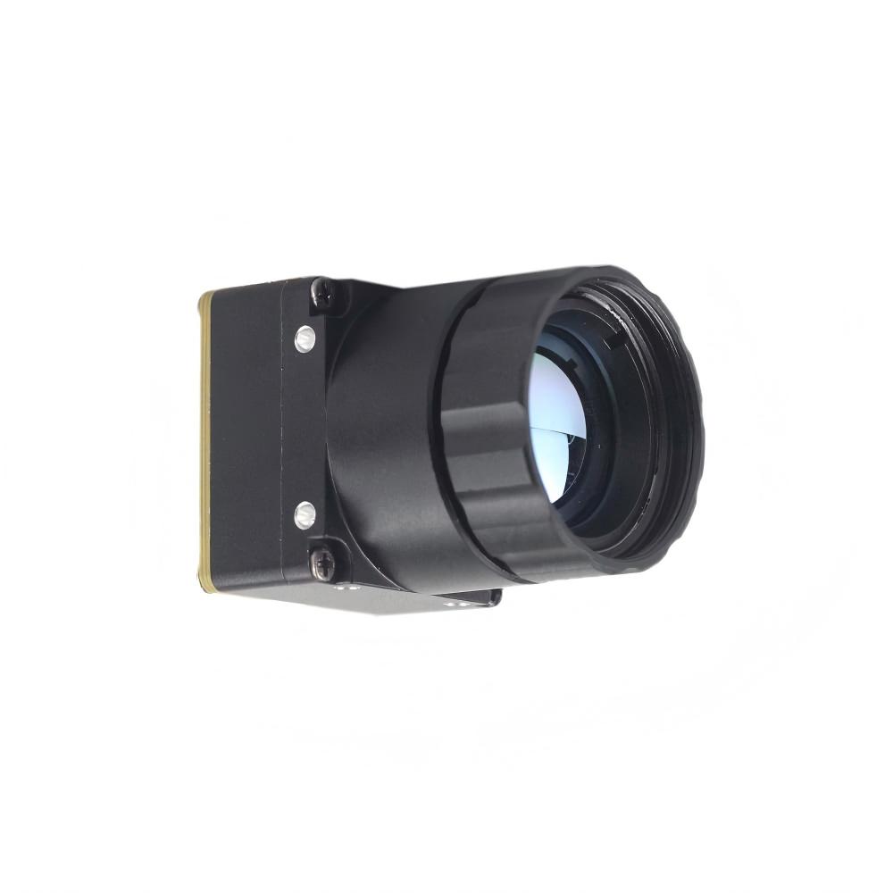
Adopting high-performance infrared detectors, the Mini 256 Uncooled LWIR Thermal Camera Module is optimized for ultra-clear thermal imaging and accurate temperature measurement. Engineered to capture infrared radiation and output a uniform thermal image with radiometry, this core is tailored for detecting ground thermal anomalies, unexploded ordnance, and buried landmines.
- ✅ Rozdzielczość: 256×192 pixel array with advanced 12μm microbolometer detector
- ⚙️ Dokładność radiometryczna: High-precision temperature calculation across the full frame with uniform thermal field mapping
- ✅ Industrial Hardening: High shock resistance and wide operating temperature profiles suitable for defense and field robotics
- ⚙️ Obudowa: Highly integrated ultra-miniature layout enabling seamless drop-in integration
Całkowity koszt posiadania (TCO) i optymalizacja BOM dla integratorów systemów
Evaluating only the initial purchase price of a thermal camera module frequently introduces unexpected integration costs later in development. Seasoned system architects track the complete Total Cost of Ownership (TCO), accounting for secondary mechanical, electrical, and computational expenses needed to bring a complete system to market.
Structural Lens Mounts and Thermal Isolation
Microbolometers are thermal sensors, meaning they are sensitive to environmental heat shifting across their internal enclosures. Parasitic thermal gradients conducted through aluminum chassis or generated by adjacent microprocessors will trigger sensor drift, causing uneven shading or false temperature spikes.
- ⚙️ Thermal Decoupling: Hardware engineers must incorporate low-thermal-conductivity standoffs (such as PEEK, Torlon, or ceramic washers) between the core and host chassis to isolate convective heat paths.
- ⚙️ Protective Windows: If deploying a thermal core in an IP67-rated enclosure (such as an external surveillance housing or mining inspection drone), standard protective sapphire or Gorilla Glass cannot be used because they block LWIR transmission. Integrators must budget for an additional anti-reflective, Diamond-Like Carbon (DLC) coated Germanium or Zinc Selenide (ZnSe) protective flat window, adding $40 to $120 to the enclosure BOM.
Micro-Solenoid Failure Rates and MTBF
Mechanical shutters used for Non-Uniformity Correction represent the only moving element in an uncooled thermal camera core. In continuous, 24/7/365 security operations, an internal shutter cycling every 3 to 5 minutes will complete roughly 100,000 to 175,000 cycles annually.
Lower-tier OEM shutters often suffer solenoid spring fatigue or coil burnout between 300,000 and 500,000 cycles, causing complete system blind-outs in less than three years. Investing in industrial-grade cores equipped with brushless magnetic actuators or robust field-proven shutterless algorithms significantly lowers field service warranty costs and reduces downstream maintenance overhead.
Edge Compute Budgeting: Linux Drivers, V4L2 & ROS Integration
Integrating a thermal module into modern robotic control loops requires robust software driver architectures:
- ⚠️ The "Closed-SDK" Trap: Many inexpensive consumer-grade thermal cores supply only precompiled Android APK files or compiled, closed-source Windows Dynamic Link Libraries (DLLs). Modifying these systems to interface with embedded Linux, the Robot Operating System (ROS 2), or standard Video4Linux2 (V4L2) kernel drivers demands reverse engineering, manual packet sniffing, and custom driver development.
- ✅ Engineering Savings with Native APIs: Paying a 15% upfront premium for enterprise-grade modules that feature open C/C++ SDKs, native MIPI-CSI kernel tree drivers, and Python bindings accelerates engineering timelines, trimming months off the software development schedule.
Szczegółowe techniczne FAQ
What drives the massive price gap between a $200 module and a $2,000+ thermal module?
Are compact 256x192 or 640x512 thermal modules suitable for Raspberry Pi or drone integration?
Does choosing a high-resolution 640x512 module drastically inflate project BOM costs?
Why are shutterless thermal camera modules gaining traction in aerospace applications?
Protokół RFQ i sourcingu dla integratorów systemów
To streamline sourcing cycles and obtain accurate volume price quotes from international core manufacturers, procurement and hardware teams should provide this comprehensive requirement profile during initial RFQ submissions:
- Target Array Specifications:
- ⚙️ Pixel Array Dimensions: 640×512, 384×288, or 256×192
- ⚙️ Pixel Pitch: 12μm vs. 17μm node
- ⚙️ Required NETD Sensitivity (@25°C, f/1.0): < 30mK, < 40mK, or < 50mK
- Konfiguracja optyczna:
- ⚙️ Desired Field of View (HFOV × VFOV in degrees) or Focal Length (mm)
- ⚙️ Lens Material: Single-point diamond turned Monocrystalline Germanium vs. Precision Molded Chalcogenide
- ⚙️ Focus Mechanism: Fixed Athermalized, Manual Threaded, or Stepper Motor Focus
- ⚙️ Window Protection: Integrated DLC/AR Germanium protective window vs. bare core
- Thermal Metrology (Radiometry):
- ⚙️ Measurement Capability: Qualitative Imaging Only, Center-Point Spot Tracking, or Full-Frame Radiometric Array
- ⚙️ Temperature Measurement Range: –20°C to +150°C (standard industrial), 0°C to +550°C (firefighting), or custom high-temp
- ⚙️ Absolute Calibration Accuracy: ±2°C / ±2% NIST-traceable vs uncalibrated raw counts
- Electrical & Mechanical Integration:
- ⚙️ Primary Output Protocol: Native MIPI-CSI-2, USB 2.0/USB-C (UVC + Y16), DVP Parallel, or UART/SPI
- ⚙️ Host OS & Architecture: Embedded Linux (Ubuntu/Debian), ROS 2, FreeRTOS, or Android
- ⚙️ Power Envelope: Maximum voltage/current limits (e.g., 3.3V–5V DC, < 0.8W)
- ⚙️ Mechanical Constraints: Maximum outer dimensions (L × W × H in mm) and total payload mass (< 20g)
- Export Licensing & Commercial Sourcing:
- ⚙️ Framerate Requirement: 9Hz Slow-Scan (Civilian Unrestricted) vs. 25Hz / 30Hz / 50Hz Fast-Scan
- ⚙️ Deployment Region & End-User Industry Classification
- ⚙️ Annual Production Forecast: Prototype Phase (1–5 units), Pilot (50–200 units), or Volume OEM (1,000+ units)
📚 Piśmiennictwo i dalsze lektury
- Standard branżowy: Wikipedia Thermal Imaging Science & Radiometry
- Standard branżowy: Arducam Embedded Machine Vision Systems & MIPI Interfaces
- Powiązany przewodnik: Thermal Imaging Cameras: Piercing Eyes in Dark Environments
- Powiązany przewodnik: Thermography: Practical Commercial Applications and Diagnostics
- Powiązany przewodnik: Industrial Thermal Imaging Cameras: Fiery Eyes for Hazard Detection