
Best Thermal Image Camera Guide: From DIY Projects to High-Res OEM Modules
2026年10月29日
Infrared Heat Camera Guide: Working Principle, IR vs. Thermal & OEM Modules
Modern predictive maintenance, automated process control, and defense-grade surveillance rely heavily on the non-contact quantification of thermal energy. An infrared heat camera functions not merely as an imaging sensor, but as an advanced optoelectronic radiometric instrument capable of translating invisible electromagnetic flux into spatial thermal matrices. Unlike standard visible-spectrum sensors that document ambient reflectance across narrow bands (0.4 to 0.7 µm), an infrared heat camera interrogates the long-wave infrared (LWIR) spectrum (8 to 14 µm). Within this band, every object above absolute zero emits electromagnetic radiation governed by Planck's radiation law, Stefan-Boltzmann mechanics, and material-specific emissivity characteristics.
Industrial deployment of this technology requires moving beyond simple thermal spot checks to embedding micro-sized, high-resolution uncooled microbolometer cores directly into automated architectures. Integrating thermal cores into unmanned aerial system (UAS) payloads, automated optical inspection (AOI) rigs, or remote security turrets demands an in-depth understanding of sensor pitch, Noise Equivalent Temperature Difference (NETD), lens focal geometries, optical coatings, and edge-compute protocol matching. This comprehensive engineering blueprint provides systems engineers, hardware integrators, and OEM developers with an engineering-grade roadmap to demystify infrared thermal sensors, delineate true thermal imaging from near-infrared photography, and select the optimal LWIR OEM core for mission-critical applications.
Содержание
- 👉 1. Working Principle: The Optoelectronic Architecture of an Infrared Heat Camera
- 👉 2. Near-Infrared (NIR) vs. Long-Wave Infrared (LWIR): Demystifying IR Terminology
- 👉 3. Thermal Optics Engineering: Germanium, Chalcogenide, and Transmission Physics
- 👉 4. Digital Interfaces & Edge-AI Integration: MIPI, USB, RJ45, and CVBS
- 👉 5. OEM LWIR Core Benchmark: Mini2 MIPI vs. ASIC RJ45/IP Modules
- 👉 6. Real-World Enterprise Deployments: UAS Inspection, PCB Thermography & Surveillance
- 👉 7. Radiometric Engineering FAQ
1. Working Principle: The Optoelectronic Architecture of an Infrared Heat Camera
An infrared heat camera operates on the fundamental physical reality that molecular thermal agitation produces spontaneous electromagnetic emission. To measure and visualize this emission, the system relies on an interconnected chain of specialized components: non-silicon specialized optics, an uncooled focal plane array (FPA), a readout integrated circuit (ROIC), and non-uniformity correction (NUC) algorithms running on an embedded digital signal processor (DSP) or dedicated application-specific integrated circuit (ASIC).
The operational sequence begins at the objective lens, which gathers thermal photons within the 8 to 14 µm spectral window and focuses them onto the focal plane array. The uncooled FPA converts the absorbed thermal flux into differential electrical signals. These signals are then sampled by the ROIC, digitized, conditioned through multi-stage calibration pipelines, and converted into visually discernible thermal palettes or calibrated 14-bit radiometric matrices containing absolute temperature values for every pixel in the field of view.
The Microbolometer Sensing Layer
At the physical core of modern industrial infrared heat cameras lies the microbolometer array. Unlike cryogenically cooled Mid-Wave Infrared (MWIR) detectors that rely on internal quantum photon detection at temperatures near 77 Kelvin, uncooled Long-Wave Infrared (LWIR) detectors operate reliably at ambient industrial temperatures without heavy, power-hungry Stirling coolers.
The active sensing surface consists of an array of micro-machined bridge pixels suspended over an underlying silicon substrate by thin structural legs. This suspended vacuum architecture provides extreme thermal isolation, preventing heat from dissipating prematurely into the structural substrate. Each individual pixel contains an absorbing layer composed typically of Vanadium Oxide (VOx) or Amorphous Silicon (a-Si). Vanadium Oxide is widely preferred in high-precision engineering environments due to its superior Temperature Coefficient of Resistance (TCR, approximately -2% to -3% per Kelvin) and lower 1/f noise characteristics, resulting in significantly higher signal-to-noise ratios and thermal sensitivity.
The physical behavior of each suspended micro-bridge is dictated by the thermodynamic heat balance equation:
C-го · (dT / dt) + G-го · ΔT = η · Popt
Где:
- ⚙️ C-го represents the thermal capacitance of the microbolometer bridge element,
- ⚙️ G-го is the thermal conductance of the micro-machined supporting legs connecting the bridge to the substrate,
- ⚙️ ΔT is the temperature elevation of the sensing bridge above the substrate baseline,
- ⚙️ η is the optical absorption efficiency within the 8 to 14 µm band, and
- ⚙️ Popt is the incident optical thermal power focused onto the pixel.
When LWIR radiation strikes the VOx micro-absorber, the material absorbs the photons, causing a measurable change in temperature within the suspended micro-bridge. This temperature delta alters the electrical resistance of the VOx film according to the formula:
ΔR = R0 · α · ΔT
Где R0 is the baseline electrical resistance, α is the material's Temperature Coefficient of Resistance, and ΔT is the thermal elevation induced by incident radiant flux.
The ROIC and Non-Uniformity Correction (NUC)
The Readout Integrated Circuit (ROIC) is bonded directly beneath the micro-machined array. It sequentially injects a precisely stabilized bias voltage across each pixel to measure minute resistance shifts. The resulting microscopic currents are integrated via Capacitive Transimpedance Amplifiers (CTIA) and transformed into analog voltages before being digitized by on-chip high-speed analog-to-digital converters (ADCs), typically operating at 14-bit or 16-bit precision.
Because semiconductor lithography and material deposition variations inevitably cause individual microbolometer bridges to have slightly different baseline resistances, responsive sensitivities, and thermal dissipation paths, the raw digitized output contains significant spatial noise known as Fixed Pattern Noise (FPN). To eliminate this artifact, the camera's processing pipeline executes a two-point Non-Uniformity Correction (NUC) using calibration coefficients derived from exposure to known uniform blackbody radiators:
Vскорректированный(i,j) = G(i,j) · [Vнеобработанный(i,j) - O(i,j)]
Где:
- ⚙️ G(i,j) is the calculated gain coefficient for pixel coordinates (i,j),
- ⚙️ O(i,j) is the individual offset coefficient recorded during exposure to a uniform thermal scene, often provided by an internal electromechanical shutter blade or a shutterless algorithmic estimation block.
Radiometric Calibration & Temperature Quantification
A true radiometric infrared heat camera does not stop at producing an 8-bit visual grayscale or color-mapped image for human viewing. It converts the corrected 14-bit digital numbers (DN) into absolute thermodynamic temperature values for every pixel. To calculate absolute target surface temperature, the internal processor computes the total radiative flux entering the aperture using the fundamental radiometric balance equation:
Wобщ = ε · τатм · σ · Tцель4 + (1 - ε) · τатм · σ · Tambient4 + (1 - τатм) · σ · Tатм4
Где:
- ⚙️ σ is the Stefan-Boltzmann constant (5.670374 × 10⁻⁸ Вт/м2K4),
- ⚙️ ε is the emissivity of the target surface (varying from 0.01 for polished aluminum to 0.98 for matte black paint),
- ⚙️ τатм represents the spectral transmission coefficient of the intermediate atmosphere,
- ⚙️ Tambient is the reflected apparent background temperature, and
- ⚙️ Tатм is the ambient air temperature along the optical measurement path.
By solving for Tцель across millions of operations per second, modern LWIR cores output high-density radiometric arrays where every single pixel represents an accurate, quantifiable thermal measurement.
2. Near-Infrared (NIR) vs. Long-Wave Infrared (LWIR): Demystifying IR Terminology
A common point of confusion in embedded hardware selection is the conflation of Near-Infrared (NIR / SWIR) imaging with Long-Wave Infrared (LWIR) thermal imaging. While both occupy regions of the electromagnetic spectrum beyond the human eye's visible sensitivity threshold (approximately 0.38 to 0.75 µm), their physical detection mechanisms, sensor architectures, optical elements, and operational utilities differ fundamentally.
The Physical Divergence: Reflection vs. Emission
The distinction between NIR and LWIR lies in the origin of the detected photons:
- ⚙️ Near-Infrared (NIR, 0.75 to 1.1 µm): Operates entirely on the principle of reflected radiation. Standard CMOS sensors fabricated on silicon wafers exhibit natural quantum efficiency extending slightly past 750 nm up to silicon's bandgap limit (approximately 1100 nm). In low-light environments, NIR security cameras require active illumination sources, such as 850 nm or 940 nm infrared LED arrays or filtered searchlights. If an object does not have external photons bouncing off its surface, an NIR camera cannot detect it. NIR cameras do not measure heat; they register the optical reflectivity of invisible light.
- ✅ Long-Wave Infrared (LWIR, 8.0 to 14.0 µm): Operates exclusively on spontaneous blackbody emission. According to Planck's distribution law and Wien's displacement law, objects at typical ambient terrestrial temperatures (-40°C to +500°C) emit radiation whose peak spectral radiant emittance sits squarely within the 8 to 14 µm window. No external illumination is required or utilized. An uncooled LWIR sensor functions in total, absolute darkness, detecting the heat radiated directly by the object itself.
Scattering Mechanics in Atmospheric Obscurants
A decisive engineering reason to deploy an LWIR infrared heat camera over an NIR camera in demanding environments is resilience to airborne obscurants such as smoke, fog, and industrial dust. This advantage is governed by Mie scattering theory.
When atmospheric particulate diameters approach the wavelength of incident radiation, scattering losses are severe. Airborne soot and wildland smoke particles typically measure between 0.5 and 1.5 µm in diameter. Because NIR wavelengths (0.75 to 1.0 µm) match these particle sizes, NIR photons undergo heavy forward and backward scattering, completely blinding NIR surveillance cameras. In contrast, LWIR wavelengths (8 to 14 µm) are approximately an order of magnitude larger than smoke and haze particles. The radiation bypasses the particulate suspension with negligible scattering, enabling thermal cameras to see through dense smoke screens, dust storms, and marine fog layers.
| Метрика / Параметр | Near-Infrared (NIR) Night-Vision Camera | Long-Wave Infrared (LWIR) Heat Camera |
|---|---|---|
| Spectral Operational Band | 0.75 – 1.1 µm (750 – 1100 nm) | 8.0 – 14.0 µm (8000 – 14000 nm) |
| Operational Source | Reflected external illumination (LEDs, moonlight) | Spontaneous blackbody heat emission |
| Архитектура детектора | Silicon CMOS / CCD Photodiode Array | Vanadium Oxide (VOx) Microbolometer Array |
| Optical Lens Substrate | Standard Crown/Flint Optical Glass, Plastics | Monocrystalline Germanium (Ge), Chalcogenide |
| Absolute Radiometric Output | No. Delivers relative luminance/reflectivity | Yes. Outputs calibrated per-pixel temperature |
| Smoke, Dust & Haze Penetration | Poor (High Mie scattering due to short wavelength) | Superior (Long wavelengths bypass micro-particles) |
Engineers often investigate whether standard commercial cameras can be modified for temperature screening. For a comprehensive architectural evaluation of silicon bandgap constraints and optical retrofits, read the detailed technical analysis on whether we can convert a regular camera into a thermal imaging camera.
3. Thermal Optics Engineering: Germanium, Chalcogenide, and Transmission Physics
One of the most consequential engineering differences between visual spectrum systems and thermal infrared instruments is the physics of optical materials. Conventional optical glass (silicon dioxide, SiO2) exhibits near-complete opacity across the 8 to 14 µm spectral band due to strong silicon-oxygen reststrahlen vibrational absorption. Placing a high-end photographic or microscope lens in front of a microbolometer creates an impenetrable barrier to thermal photons. As a result, infrared heat camera lenses require specialized optical substrates.
Монокристаллический германий (Ge)
Germanium is the traditional material of choice for high-resolution LWIR optical design:
- ⚙️ Refractive Index: Germanium boasts an extraordinarily high refractive index of approximately 4.002 at 10.6 µm. This high refractive power allows optical engineers to design fast, low-aberration singlet and doublet lenses with minimal surface curvature and compact barrel lengths.
- ✅ Transmission Characteristics: When uncoated, Germanium reflects roughly 36% of incident light per surface due to Fresnel reflection losses. However, when treated with multi-layer High-Efficiency Anti-Reflective (HEAR) and exterior Diamond-Like Carbon (DLC) hard coatings, internal transmission routinely exceeds 95% across the full LWIR band. DLC coatings provide severe-environment resistance against sand abrasion, saltwater immersion, and acidic industrial airborne chemicals.
- ⚠️ Thermal Drift & Thermal Runaway: A major limitation of Germanium is its high thermo-optic coefficient (dn/dT ≈ 3.96 × 10⁻⁴ K-1). As temperature fluctuates, the focal point shifts rapidly, demanding active mechanical or passive optical athermalization. Furthermore, as Germanium heats up past +60°C to +80°C, thermal energy promotes valence electrons into the conduction band. This free-carrier absorption triggers thermal runaway, rendering the lens element virtually opaque to LWIR radiation.
Chalcogenide Glass Compounds
To overcome the thermal limitations and high raw-material costs of monocrystalline Germanium, optical engineers increasingly deploy Chalcogenide glasses (amorphous compounds containing sulfur, selenium, or tellurium, such as Ge28Sb12Se60 or GASIR):
- ⚙️ Refractive Index & Dispersion: Chalcogenide glasses feature refractive indices ranging between 2.5 and 2.8, offering balanced chromatic dispersion characteristics.
- ✅ Athermal Optical Design: Chalcogenides have a much lower dn/dT coefficient than Germanium. By pairing a Chalcogenide optical element with an aluminum or plastic lens barrel whose thermal expansion rate naturally offsets the glass's optical shift, engineers can build passively athermalized lenses that stay perfectly focused from -40°C to +85°C without motorized focus mechanisms.
- ✅ Precision Glass Molding (PGM): While Germanium must be slowly shaped via Single Point Diamond Turning (SPDT), Chalcogenide glass can be precision molded into complex aspheric and diffractive geometries at scale. This substantially lowers unit costs in high-volume OEM manufacturing.
Optical Speed: The Decisive Role of the f-Number
Thermal optical engineering requires strict attention to the lens speed, represented by the f-number (F/# = focal length / entrance pupil diameter). The radiant optical power (Popt) delivered onto each microbolometer pixel is inversely proportional to the square of the optical system's f-number:
Edetector = π · Lscene / [4 · (F/#)2 + 1]
Because the signal-to-noise ratio and Noise Equivalent Temperature Difference (NETD) degrade quadratically as the aperture constricts, an F/1.0 optical system delivers four times more thermal flux to the microbolometer than an F/2.0 optic. In thermal imaging—where subtle scene temperature deltas may be as small as 0.04°C (40 mK)—maintaining a fast lens aperture between F/1.0 and F/1.2 is essential to preserve radiometric measurement precision.
4. Digital Interfaces & Edge-AI Integration: MIPI, USB, RJ45, and CVBS
When selecting an uncooled LWIR core for embedded system design, choosing the correct physical layer and streaming protocol is vital. Systems engineers must balance data latency, frame throughput, processing overhead on the host computer, power envelope constraints, and physical cabling topology.
1. MIPI-CSI-2 (Mobile Industry Processor Interface)
The MIPI Camera Serial Interface 2 (CSI-2) is the industry standard for low-latency, SWaP-constrained (Size, Weight, Power, and Cost) robotic systems, unmanned aerial vehicles (UAVs), and portable inspection devices:
- ⚙️ Architecture: Sensor data travels over differential D-PHY lines directly into the host application processor's Image Signal Processor (ISP) or GPU memory through Direct Memory Access (DMA). This bypasses the serialization and deserialization overhead inherent to network protocols.
- ✅ Edge-AI Synergy: MIPI delivers uncompressed raw 14-bit or 16-bit radiometric data frames straight to embedded computing modules such as the NVIDIA Jetson Orin Nano, Xavier, or Raspberry Pi Compute Modules. This makes it ideal for real-time edge AI tasks like object detection, autonomous drone navigation, and thermal anomaly tracking.
- ⚙️ Mechanical Considerations: MIPI traces require tight impedance control and have a limited reach (typically under 20 to 30 cm) before high-frequency degradation sets in. System designers rely on micro-coaxial ribbons or high-density board-to-board connectors engineered by Molex to maintain signal integrity within tightly packaged drone gimbals.
2. RJ45 / IP Ethernet (RTSP / ONVIF)
For industrial automation, predictive maintenance, and perimeter defense networks, the RJ45 Ethernet interface remains the gold standard:
- ⚙️ On-Board ASIC Compression: The thermal core features an integrated video processing ASIC that executes NUC, applies false-color palettes, and encodes the raw video stream into standard H.264, H.265, or MJPEG compression formats.
- ✅ Transmission Distance: Standard Cat5e or Cat6 twisted-pair cabling reliably carries power and thermal video over runs up to 100 meters without active signal repeaters. Using Power-over-Ethernet (PoE / IEEE 802.3af) simplifies field deployment to a single cable run.
- ✅ Protocol Compliance: These cores stream video using the Real-Time Streaming Protocol (RTSP) and adhere to ONVIF (Profile S/G/T) standards. Radiometric metadata is either embedded directly in H.264 Supplemental Enhancement Information (SEI) frames or polled through dedicated HTTP REST APIs and Modbus-TCP endpoints.
3. USB 2.0 / USB 3.0 (UVC)
USB interfaces offer a balanced approach for PC-tethered test fixtures, medical diagnostic systems, and benchtop analysis tools:
- ✅ Driverless Interoperability: By adhering to the USB Video Class (UVC) protocol, the thermal core functions out of the box across Linux, Windows, and Android operating systems without requiring custom kernel drivers.
- ⚙️ Data Modes: USB cores generally support two simultaneous modes: an 8-bit color-mapped YUV/RGB stream for display monitors, and a 16-bit packed Y16 radiometric stream containing raw ADC digital values for software-based temperature calibration. Integrators pursuing USB-centric embedded designs can examine the technical specifications of the 640x512 USB LWIR embedded module.
4. CVBS (Analog Composite Video)
Analog CVBS (NTSC/PAL) remains relevant in weight-critical, low-latency applications:
- ✅ Zero Latency: Converting the sensor's digital frames into an interlaced analog signal provides instantaneous video output with near-zero latency, avoiding the encoding and buffering delays of digital pipelines.
- ⚠️ Legacy Gimbals & FPV: Analog video links are widely used in long-range drone FPV systems and legacy defense equipment. However, CVBS discards all absolute per-pixel radiometric temperature data, limiting its use strictly to human visual observation.
5. OEM LWIR Core Benchmark: Mini2 MIPI vs. ASIC RJ45/IP Modules
When selecting an uncooled LWIR core, systems integrators must balance Size, Weight, Power, and Cost (SWaP-C) against optics, processing performance, and connectivity. Below, we examine two industrial 640×512 VOx microbolometer modules tailored for contrasting deployment scenarios. For broader system architecture guidance on selecting detector resolutions, pixel pitches, and DORI ranges, consult the comprehensive thermal camera core selection guide.
Product Profile 1: Mini2 640x512 9mm MIPI Thermal Imaging Camera Module
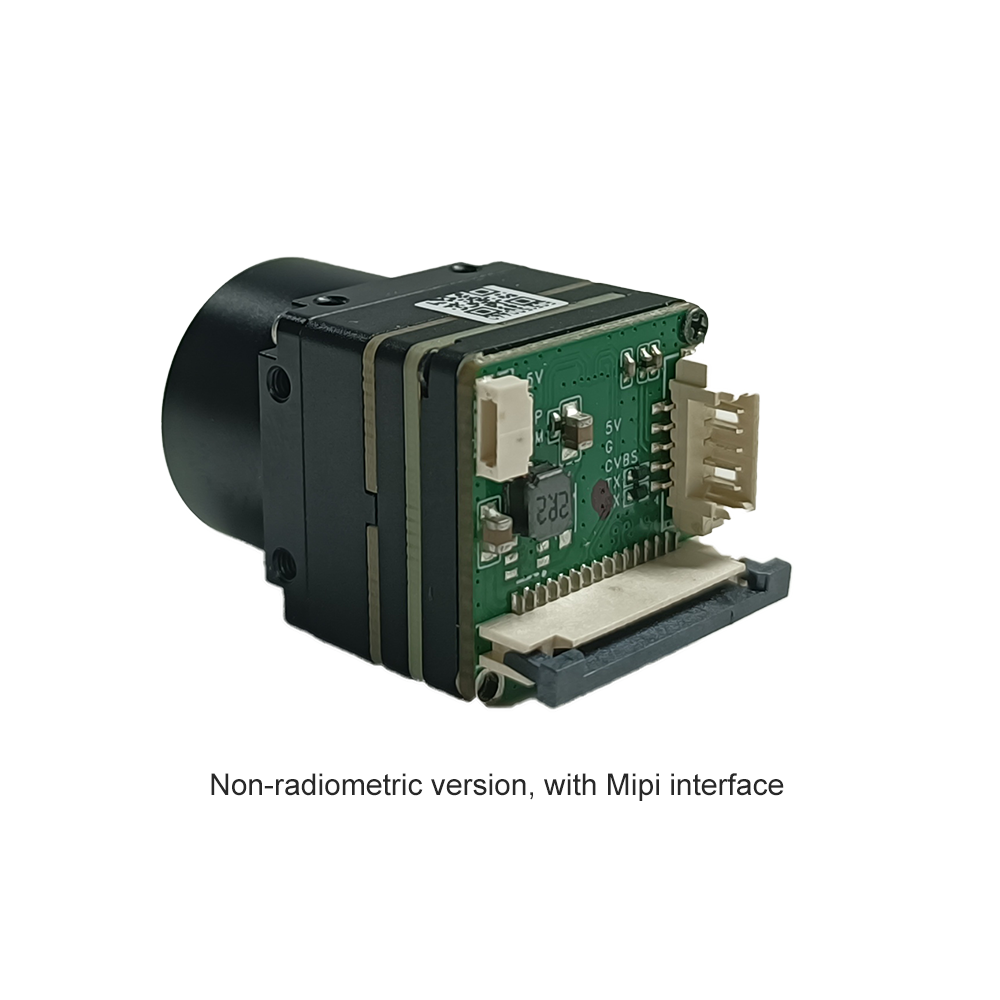
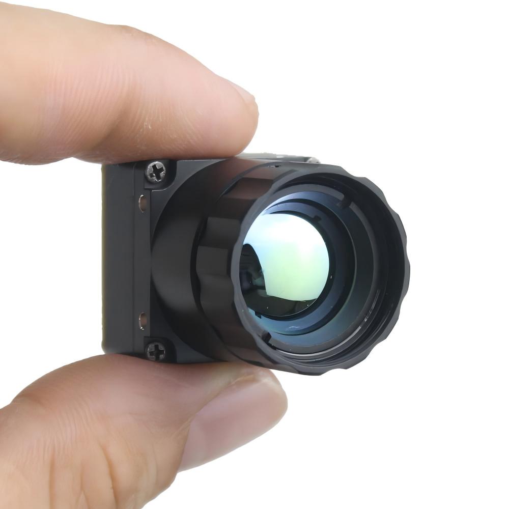
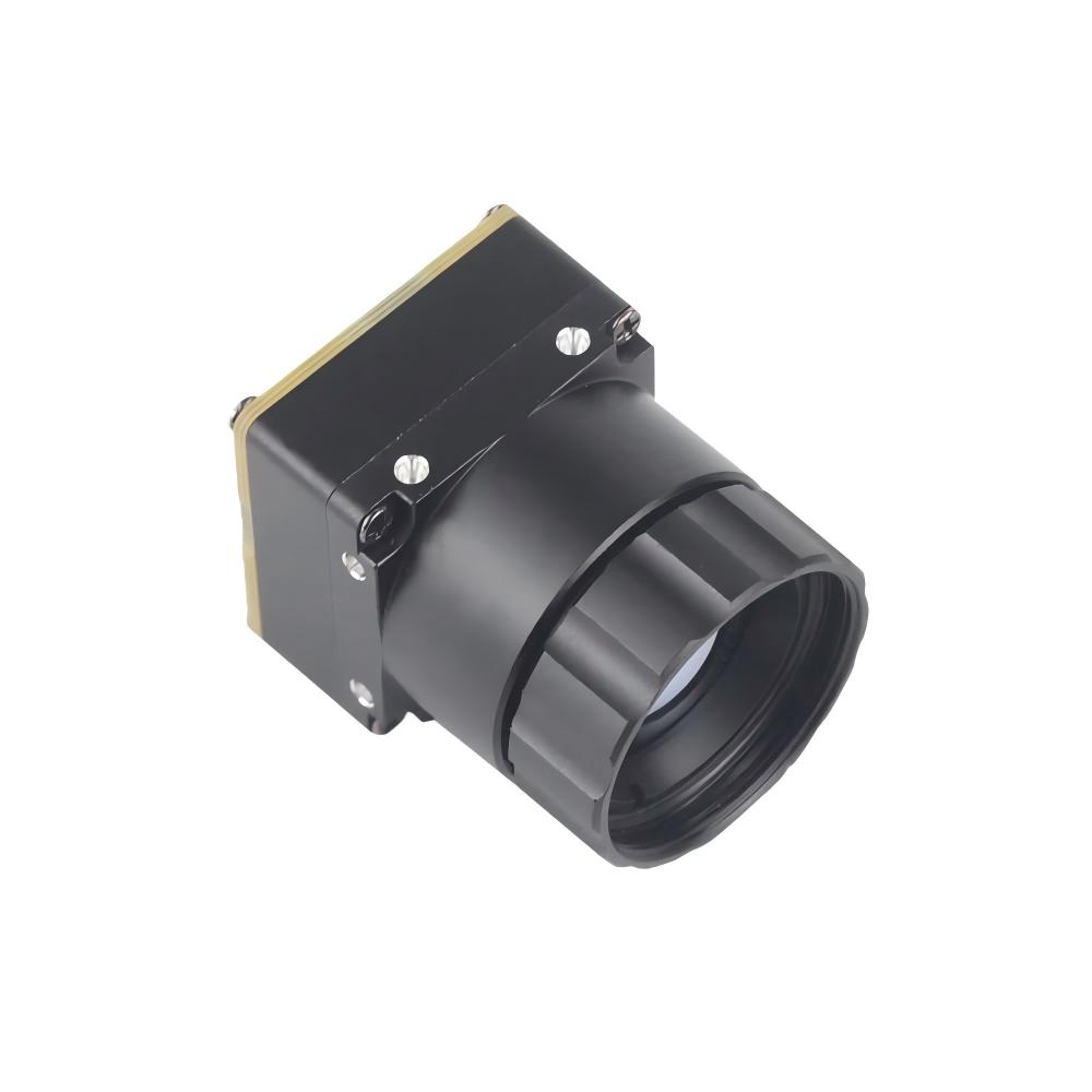
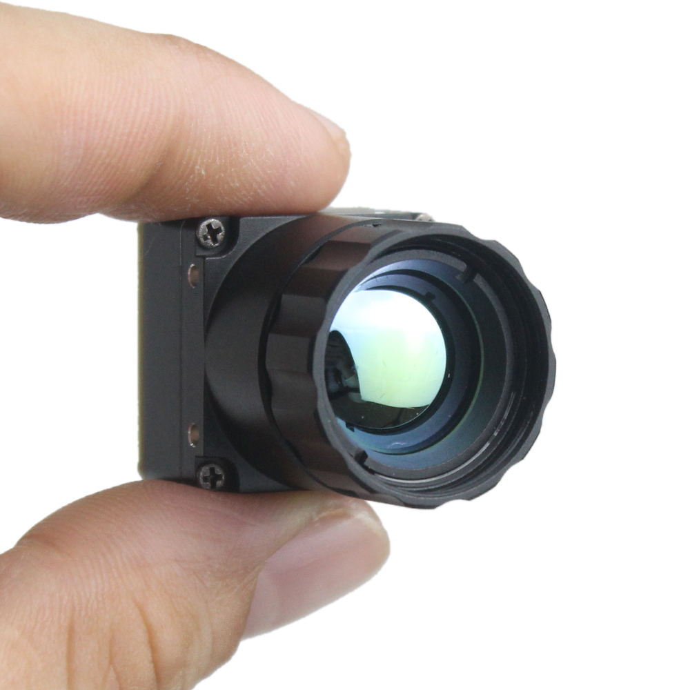
The → Неохлаждаемый инфракрасный мини-модуль тепловизионной камеры Mini2 640x512 9 мм для дронов is an ultra-compact, high-performance OEM thermal sensor core engineered for lightweight UAV payloads and mobile robotic systems. Built around an uncooled VOx microbolometer with a 12 µm pixel pitch and high thermal sensitivity (≤40 mK), this module delivers sharp, high-contrast imagery even under low-contrast conditions.
Equipped with an integrated 9.1 mm athermalized lens and a high-speed MIPI-CSI-2 interface, the Mini2 streams uncompressed raw radiometric data directly into onboard edge AI processors like the NVIDIA Jetson. This architecture eliminates the latency and weight of external encoder boards, making it ideal for drone gimbals, search-and-rescue systems, and compact optical payloads.
Product Profile 2: Uncooled Infrared RJ45 CVBS RTSP IP 640*512 ASIC Thermal Sensor Module
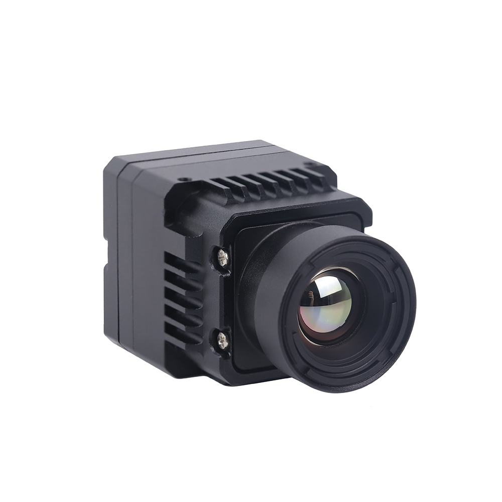
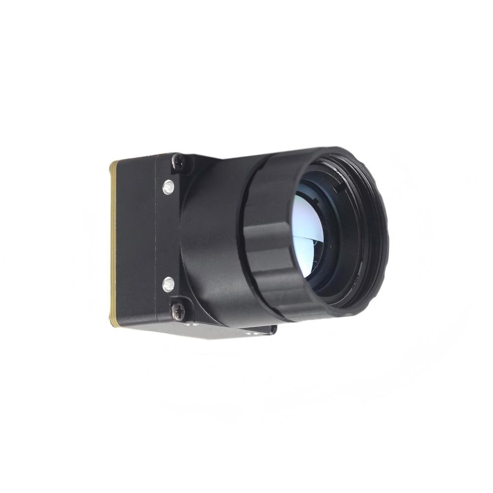
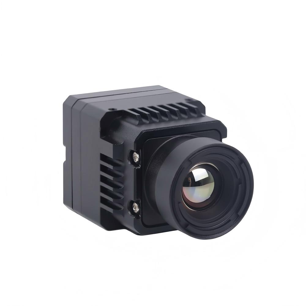
The → Uncooled Infrared Mini 640*512 ASIC Thermal Imaging Camera Module provides an all-in-one network imaging and processing solution for fixed perimeter security, automated factory inspection, and predictive maintenance. Featuring an onboard video-processing ASIC, this module handles Non-Uniformity Correction, dynamic range compression, and H.264/H.265/MJPEG encoding directly on the core.
With concurrent RJ45 Ethernet (RTSP / ONVIF Profile S) and analog CVBS composite video outputs, the ASIC 640 core integrates smoothly into modern IP-based surveillance networks and legacy analog systems alike. It supports user-configurable regions of interest, automated temperature alarms, and web-based management, making it an excellent drop-in sensor for SCADA systems and remote substations.
Direct Engineering Comparison Matrix
| Параметр спецификации | Mini2 640x512 MIPI Camera Module | ASIC 640x512 RJ45/IP Thermal Module |
|---|---|---|
| Разрешение сенсора | 640 × 512 pixels (327,680 effective nodes) | 640 × 512 pixels (327,680 effective nodes) |
| Detector Type & Pitch | Uncooled VOx Microbolometer (12 µm pitch) | Uncooled VOx Microbolometer (12 µm pitch) |
| Спектральный диапазон | 8 – 14 µm (LWIR) | 8 – 14 µm (LWIR) |
| Тепловая чувствительность (NETD) | ≤ 40 mK (@ F/1.0, 300K, 25Hz) | ≤ 40 mK (@ F/1.0, 300K, 25Hz) |
| Standard Optical Lens | 9.1 mm Athermalized Germanium / Chalcogenide | Configurable Fixed Focus (Optional 9mm / 15mm / 25mm) |
| Native Output Interfaces | MIPI-CSI-2 (4-lane/2-lane configurable) / I2C / SPI | RJ45 Ethernet (IP / RTSP) + Analog CVBS (Composite) |
| Network / Comm Protocols | Direct Linux V4L2 raw frames, Embedded DMA | ONVIF Profile S, RTSP, HTTP API, Pelco-D, UDP/IP |
| SWaP-C Characterization | Ultra-compact footprint; minimal payload weight; sub-watt power | Rugged enclosure; integrated video encoder and network engine |
| Основные целевые применения | UAS multi-rotors, micro-stabilized gimbals, wearable edge devices | Perimeter security, fixed industrial substation monitoring, SCADA vision |
6. Real-World Enterprise Deployments: UAS Inspection, PCB Thermography & Surveillance
High-resolution uncooled infrared heat cameras provide valuable, non-destructive diagnostic capabilities across industrial, aerospace, and electrical engineering environments.
1. High-Resolution Drone Payloads (UAS Inspection)
Integrating the Модуль Mini2 640x512 MIPI into small unmanned aerial systems enables autonomous aerial utility inspections. Electrical transmission grid infrastructure requires continuous monitoring of high-voltage lines, disconnect switches, and splice sleeves for abnormal thermal deltas.
A high micro-ohm contact resistance fault generates localized heating according to Joule's first law (P = I2R). Flying an automated corridor mission at an altitude of 30 meters with a 9.1 mm optic provides a wide field of view along with sufficient ground resolved distance (GRD) to identify failing distribution connectors exhibiting as little as a 5°C rise over ambient. By capturing these anomalies early, operators prevent catastrophic arc faults and transmission drop-outs.
Similarly, in multi-megawatt solar photovoltaic installations, MIPI cores connected directly to edge AI companion computers can run convolutional neural networks (CNNs) in real time to locate panel defects. Hotspots caused by cracked solar cells, internal delamination, and failed bypass diodes show up clearly as sharp thermal anomalies against the cooler, functional cells.
2. Automated Circuit Board (PCBA) Thermography
During hardware prototyping and automated bench production testing, the infrared heat camera serves as an essential tool for circuit diagnostics. Power-rail shorts, undersized ground planes, and defective surface-mount capacitors create localized thermal dissipation hotspots.
Using high-resolution 640×512 radiometric arrays allows test engineers to map thermal gradients across dense multi-layer PCBAs down to individual surface-mount packages (e.g., 0402 or 0201 passives). By monitoring the transient thermal curve during initial board power-up, test systems can catch sub-surface short circuits before board components sustain irreversible overcurrent damage.
3. Continuous Industrial Infrastructure & Perimeter Surveillance
Fixed installations, such as electrical substations, gas flare stacks, and remote borders, benefit most from the ASIC 640x512 RJ45/IP Thermal Module.
In electrical substations, transformer bushings and high-voltage capacitor banks run hot prior to structural failure. The IP core's on-board ASIC can continuously evaluate user-defined region-of-interest (ROI) bounding boxes. If the peak temperature in a transformer terminal block exceeds an alert threshold, the camera's firmware triggers automated alarms across the industrial network via ONVIF, Pelco, or REST APIs—alerting operators without requiring continuous manual monitoring.

7. Radiometric Engineering FAQ
What is the operational difference between an infrared heat camera and infrared photography?
Can an infrared heat camera completely replace a single-spot IR pyrometer?
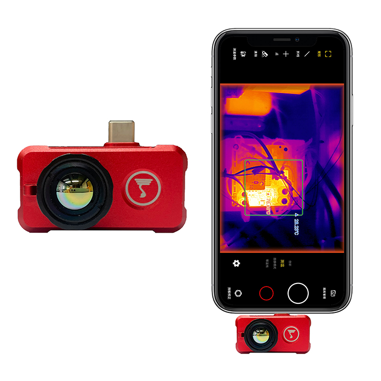
Can a mobile software app turn my commercial smartphone into an infrared heat camera?
📚 Ссылки и дополнительная литература
- Отраслевой стандарт: Edge-AI processor pairing and compute architecture via NVIDIA Jetson
- Отраслевой стандарт: High-density micro-coaxial interconnect guidelines by Molex
- Связанное руководство: Can We Convert a Regular Camera into a Thermal Imaging Camera?
- Связанное руководство: Thermal Camera Core Selection: High-Performance 640 & 384 LWIR Modules Guide
- Связанное руководство: Embedded 640x512 USB LWIR Thermal Camera Core Technical Blueprint