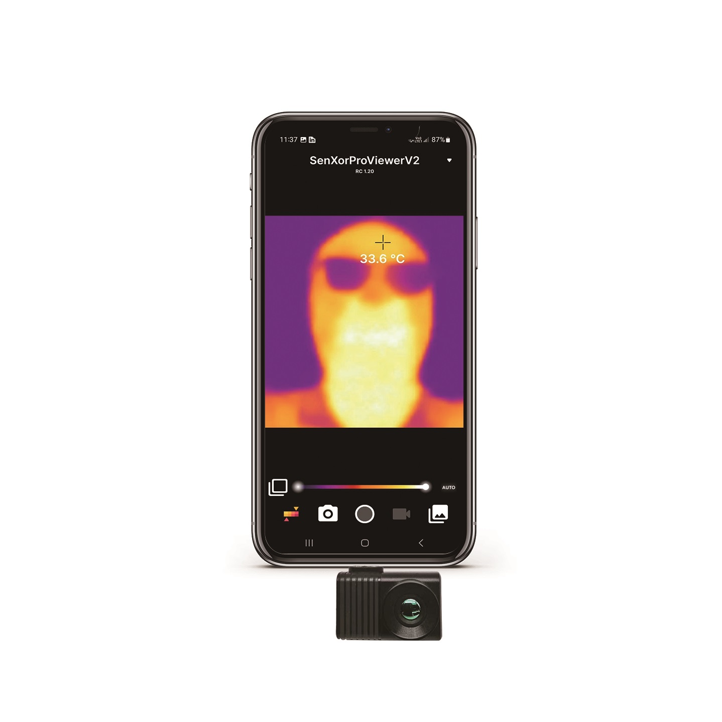
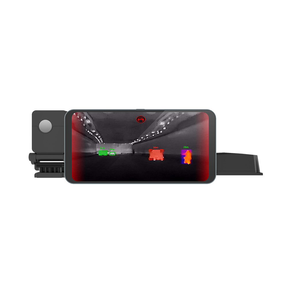


How to Choose the Best Infrared Camera Module: OEM Integration Guide for Drones & Embedded AI
2026年10月13日
Thermal Camera Guide: How It Works, Value Analysis, and OEM Module Integration
2026年10月14日
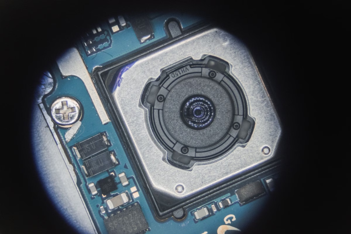
MIPI Thermal Camera Module: High-Res Embedded LWIR Cores for Drones & Edge AI
In autonomous robotic platforms, unmanned aerial vehicles (UAVs), and edge-computing vision arrays, image acquisition latency and SWaP-C (Size, Weight, Power, and Cost) constraints dictate mission success. Traditional thermal payloads that rely on USB 3.0 bridge controllers, Ethernet interfaces, or legacy analog CVBS convert digital long-wave infrared (LWIR) microbolometer output through multiple protocol translation layers. This introduces substantial processing latency, frame transmission jitter, CPU thread preemption, and parasitic board-level power dissipation. A native MIPI thermal camera module bypasses peripheral bridge ICs entirely by feeding uncompressed, 14-bit or 16-bit radiometric pixel streams directly into the host System-on-Chip (SoC) via the Mobile Industry Processor Interface Camera Serial Interface 2 (MIPI CSI-2) protocol.
By interfacing microbolometer detector arrays directly to native hardware D-PHY physical receivers on platforms like NVIDIA Jetson, Rockchip RK3588, NXP i.MX8, and Raspberry Pi Compute Module 4 (CM4), embedded systems engineers unlock Direct Memory Access (DMA) pipeline streaming without host CPU intervention. This architectural paradigm facilitates sub-millisecond frame acquisition latencies, deterministic temporal synchronization for multi-spectral sensor fusion, and zero-copy hardware memory access essential for running real-time Convolutional Neural Networks (CNNs) and Vision Transformers (ViTs) at the physical edge.
Table of Contents
- 👉 1. MIPI CSI-2 Architecture for Long-Wave Infrared (LWIR) Sensors
- 👉 2. Interface Protocol Benchmark: MIPI CSI-2 vs. USB 3.0, GigE Vision, and CVBS
- 👉 3. Embedded Hardware Pipeline: Direct Memory Access (DMA) & Zero-Copy Edge AI
- 👉 4. Purpleriver MINI Series MIPI Thermal Core Specifications & Selection Matrix
- 👉 5. Radiometric Signal Processing: Non-Uniformity Correction (NUC) and Calibrated Telemetry
- 👉 6. Hardware Carrier Design: High-Speed Differential Routing and Connector Standards
- 👉 7. Frequently Asked Questions: Embedded Systems & Engineering Integration
1. MIPI CSI-2 Architecture for Long-Wave Infrared (LWIR) Sensors
The internal architecture of a native MIPI CSI-2 uncooled thermal camera core departs fundamentally from conventional visible-spectrum CMOS sensors. An uncooled Long-Wave Infrared (LWIR) core relies on a Vanadium Oxide (VOx) or Amorphous Silicon (α-Si) microbolometer Focal Plane Array (FPA). Rather than detecting photon-induced electron transitions in silicon p-n junctions, each microbolometer pixel absorbs thermal radiation between 8 μm and 14 μm, changing its physical electrical resistance as a function of temperature.
Beneath the microbolometer matrix sits the Readout Integrated Circuit (ROIC). The ROIC utilizes column-parallel integrators and low-noise 14-bit or 16-bit analog-to-digital converters (ADCs) to sample the resistance variations across every pixel. From the ROIC, raw digitization counts are piped into an ultra-low-power field-programmable gate array (FPGA) or an application-specific integrated circuit (ASIC). This onboard processing engine handles baseline corrections: two-point Non-Uniformity Correction (NUC), dynamic Bad Pixel Replacement (BPR), and Digital Detail Enhancement (DDE).
Once corrected, the data enters the MIPI CSI-2 transmitter protocol layer. Here, pixel streams are packetized into dedicated byte sequences and driven through a MIPI D-PHY physical layer directly to the host SoC over differential striplines.
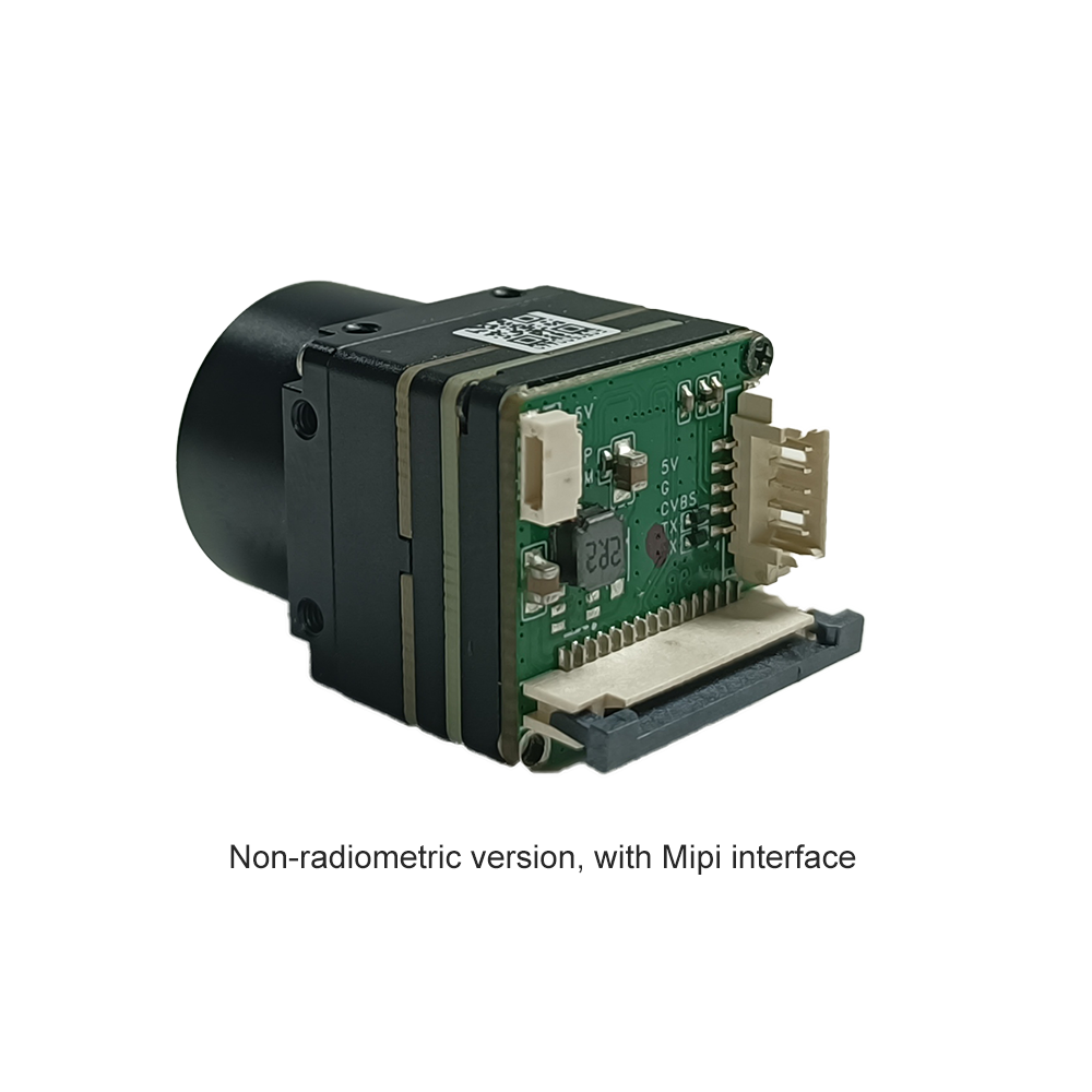
Physical Layer (D-PHY) Signaling Mechanics
The transmission interface utilizes the MIPI Alliance D-PHY specification, an asynchronous, source-synchronous architecture optimized for low-power, point-to-point interconnects. D-PHY operates across two distinct operational modes on the same physical pins:
- ⚙️ High-Speed (HS) Mode: Employs low-voltage differential signaling (SLVS) with a nominal differential voltage swing of 200 mV centered at a 200 mV common-mode ground level (operating between 100 mV and 300 mV). HS mode transmits payload data at bitrates from 80 Mbps up to 1.5 Gbps per lane, maximizing high-throughput delivery while preserving low RF emissions.
- ⚙️ Low-Power (LP) Mode: Transitions to single-ended, 1.2V CMOS-level signaling. LP mode manages line control states, protocol handshaking, Ultra-Low Power State (ULPS) transitions, and frame-boundary demarcations with minimal parasitic draw.
The clock distribution employs a dedicated differential Double Data Rate (DDR) clock lane accompanying one or two differential data lanes. In a dual-lane configuration, byte streams alternate across Data Lane 0 and Data Lane 1. For an uncooled 640×512 microbolometer running at 60 Hz with 16-bit radiometric transmission, the required aggregate bandwidth is calculated as:
Including CSI-2 packet framing, line synchronization, and vertical blanking overhead (typically 15% to 20%), the total interface bandwidth tops out near 375 Mbps. A single D-PHY lane operating at 800 Mbps easily accommodates this throughput. Splitting this stream across two differential lanes operating at 400 Mbps allows hardware engineers to drop the operational clock frequency, dramatically suppressing electromagnetic interference (EMI) within sensitive GPS and RF transceiver bands on drone airframes.
Packet Structuring, Data Types, and Virtual Channels
The MIPI CSI-2 protocol organizes the thermal data pipeline into structured packet layers:
- ⚙️ Short Packets (4 Bytes): Contain an 8-bit Data Identifier (DI), a 16-bit frame count or line count, and an 8-bit Error Correction Code (ECC). Short packets signal Frame Start (FS, DI =
0x00) and Frame End (FE, DI =0x01), marking the precise exposure intervals of the thermal microbolometer. - ⚙️ Long Packets (Payload Variable): Encapsulate individual horizontal thermal raster lines. A Long Packet consists of a 4-byte header (DI, 16-bit Word Count, ECC), the payload data bytes, and a 2-byte 16-bit Cyclic Redundancy Check (CRC) footer for detecting single- and multi-bit transmission errors.
The DI byte specifies the exact sensor formatting through standard MIPI Data Types (DT):
- ⚙️ RAW14 (
DT 0x2D) or RAW16 (DT 0x2E): Delivers absolute linear digital counts directly proportional to microbolometer surface flux. This is the mode utilized for scientific radiometry, precision agricultural mapping, and edge predictive maintenance. - ⚙️ YUV422 8-bit (
DT 0x1E): Delivers AGC-processed, tone-mapped video for immediate rendering on pilot ground control stations (GCS) or analog downlink transmitters without requiring host-side contrast stretching. - ⚙️ User-Defined Data Types (
DT 0x30through0x37): Allows interleaving of embedded telemetry lines. The thermal core injects internal FPA temperature sensor readouts, ROIC substrate thermistor telemetry, current shutter status, and camera configuration flags directly into auxiliary lines above or below the image payload.
Using MIPI Virtual Channel (VC) identifiers (from 0 to 3), a single physical connection can multiplex raw 14-bit radiometric frames on VC0 alongside processed 8-bit display video on VC1. This dual-stream delivery removes the need for two separate cameras or complex software transcoding on the host processor.
2. Interface Protocol Benchmark: MIPI CSI-2 vs. USB 3.0, GigE Vision, and CVBS
Thermal imaging cores deployed in edge vision systems have historically relied on USB 3.0 (UVC), industrial Gigabit Ethernet (GigE Vision), or legacy analog composite (CVBS). While these interfaces offer plug-and-play prototyping or compatibility with long cable runs, their architectural trade-offs make them ill-suited for SWaP-constrained, real-time aerial and robotic autonomy.
| Architectural Metric | Native MIPI CSI-2 | USB 3.0 / UVC | GigE Vision | Analog CVBS |
|---|---|---|---|---|
| Transport Latency | < 1.0 ms (Line-based) | 15.0 ms – 45.0 ms | 20.0 ms – 50.0 ms | > 20 ms (Digitization lag) |
| Host Interface Path | Direct SoC D-PHY / DMA | USB Host Controller (xHCI) | Ethernet MAC & IP Stack | External Analog Video ADC |
| Host CPU Overhead | 0% – 2% (Hardware DMA) | 12% – 25% (Kernel polling) | 10% – 20% (Socket processing) | 5% – 10% (Capture engine) |
| Interconnect Mass | < 1.5 grams (FPC cable) | 15 – 35 grams (Copper/jack) | 25 – 60 grams (RJ45/Cat5e) | 8 – 15 grams (Coax cable) |
| Interface Power Dissipation | < 50 mW | 350 mW – 750 mW | 800 mW – 1500 mW | 150 mW – 300 mW |
| Radiometric Precision | Full 14-bit / 16-bit Raw | Full 14-bit (Custom UVC) | Full 14-bit (GenICam) | None (8-bit lossy AGC) |
| Connector Mechanical Stability | Board-to-Board / Locking FPC | Friction-fit (Vibration risk) | Latch/Screw-lock RJ45 | Micro-coax / Soldered pin |
The architectural superiority of MIPI CSI-2 is rooted in its low-level hardware integration. When using USB 3.0, the native parallel or MIPI stream from the thermal core must pass through a bridge IC (such as an Infineon CX3 or Cypress FX3 controller). This bridge chip repackages video into Universal Video Class (UVC) USB packets, traversing the host's Extensible Host Controller Interface (xHCI), triggering system interrupts, and moving through the OS kernel network/USB stack before reaching application memory. This creates transport jitter ranging from 15 to 45 milliseconds.
Even more critical for drone gimbals is parasitic thermal dissipation. A USB bridge controller burns between 350 mW and 750 mW of power, while a GigE PHY consumes over 1 Watt. In a sealed 3-axis mini-gimbal, this localized heat radiates directly into the uncooled microbolometer housing. Because uncooled bolometers depend on micro-Kelvin thermal equilibrium, localized heat sources cause thermal drift across the FPA. This triggers frequent Non-Uniformity Correction (NUC) shutter recalibrations, which freeze the video stream during critical flight maneuvers.
Eliminating bridge ICs via a direct MIPI CSI-2 interface preserves thermal calibration stability, slashes power draw to less than 50 mW for the transport physical layer, and saves up to 50 grams of payload mass. For an exhaustive analysis of edge system trade-offs, refer to our guide on high-performance thermal imaging module integration for edge AI & UAV OEM.
3. Embedded Hardware Pipeline: Direct Memory Access (DMA) & Zero-Copy Edge AI
The primary advantage of deploying a MIPI thermal camera module in artificial intelligence pipelines is Zero-Copy memory handling. In embedded System-on-Chips sharing unified physical memory—such as the NVIDIA Jetson Orin Nano/AGX (Tegra architecture) or Rockchip RK3588—the MIPI CSI-2 receiver places arriving scanlines directly into physical DRAM via dedicated hardware Direct Memory Access (DMA) engines.
Linux Kernel Driver Architecture & V4L2 Subsystem
Under embedded Linux, Purpleriver MIPI thermal camera modules interface via the Video4Linux2 (V4L2) driver framework and the Linux Media Controller API. The thermal core registers as two logical entities: an I2C client device responsible for runtime command and control (gain state switching, manual NUC triggering, calibration curve loading, digital zoom) and a V4L2 subdevice driving the MIPI CSI-2 transmitter.
The integration begins in the board Device Tree source files (.dtsi), which map the physical hardware topology. The device tree defines the CSI port binding, the data lane mapping, the differential clock frequency, and the reset/power-down GPIOs:
// Device Tree node snippet for Jetson / RK3588 integration
&csi_port0 {
    status = "okay";
    endpoint {
        remote-endpoint = <&purpleriver_thermal_out>;
        bus-type = <4>; // MIPI CSI-2 D-PHY
        clock-lanes = <0>;
        data-lanes = <1 2>;
        link-frequencies = /bits/ 64/ <400000000>;
    };
};

i2c@3180000 {
    purpleriver_thermal: thermal-core@18 {
        compatible = "purpleriver,mini-thermal";
        reg = <0x18>;
        reset-gpios = <&gpio 42 GPIO_ACTIVE_LOW>;
        power-gpios = <&gpio 43 GPIO_ACTIVE_HIGH>;

        port {
            purpleriver_thermal_out: endpoint {
                remote-endpoint = <&csi_port0>;
                data-lanes = <1 2>;
            };
        };
    };
};
Zero-Copy DMA Buffer Sharing to CUDA & TensorRT
To run object detection networks (e.g., YOLOv8-Thermal, MobileNet-SSD) at high frame rates, CPU memory copying (memcpy) must be eliminated. By utilizing the Linux DMA-BUF subsystem, the allocated V4L2 ring buffers are shared directly with GPU/NPU memory contexts without transferring data across user-space boundaries.
The sequence follows three main operational steps:
- ⚙️ Buffer Allocation: The user application initializes the V4L2 capture device with the
V4L2_MEMORY_MMAPorV4L2_MEMORY_DMABUFallocation flag, generating physical contiguous frame buffers inside DRAM. - ⚙️ File Descriptor Export: Every buffer yields a unique file descriptor via the
VIDIOC_EXPBUFioctl call, mapping direct kernel memory handles. - ⚙️ Direct Hardware Binding: The descriptor is imported directly into deep learning engines. On NVIDIA Jetson platforms, the file descriptor maps into CUDA device memory via
cudaImportExternalMemory(), while computer vision pipelines wrap the buffer directly via OpenCV matrix headers without reallocating heap memory.
// C++ Zero-Copy Wrapping of 14-bit Radiometric Frame into OpenCV
struct v4l2_buffer buf = {0};
buf.type = V4L2_BUF_TYPE_VIDEO_CAPTURE;
buf.memory = V4L2_MEMORY_MMAP;
ioctl(v4l2_fd, VIDIOC_DQBUF, &buf);

// Wrap physical memory buffer into cv::Mat header without copying data
void* raw_kernel_ptr = buffer_mmap_ptrs[buf.index];
cv::Mat thermal_14bit(512, 640, CV_16UC1, raw_kernel_ptr);

// Direct pointer passage to TensorRT input tensor on unified memory
cudaExternalMemoryHandleDesc memDesc = {};
memDesc.type = cudaExternalMemoryHandleTypePosixFd;
memDesc.handle.fd = dma_buf_fds[buf.index];
memDesc.size = 640 * 512 * sizeof(uint16_t);
cudaImportExternalMemory(&extMem, &memDesc);

// Re-queue buffer immediately back to V4L2 capture queue
ioctl(v4l2_fd, VIDIOC_QBUF, &buf);
This unified pipeline delivers frame ingestion latencies under 1 millisecond. By freeing the host CPU from copying pixel data, system threads remain available for path planning, flight stabilization, and object tracking. To explore module selection strategies for embedded AI processing, review our AI thermal camera selection guide for high-precision OEM modules.
4. Purpleriver MINI Series MIPI Thermal Core Specifications & Selection Matrix
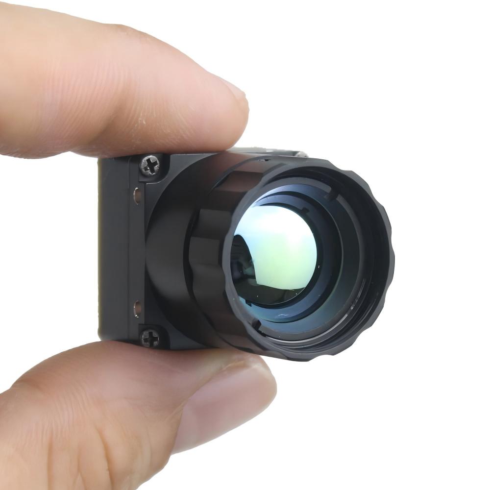
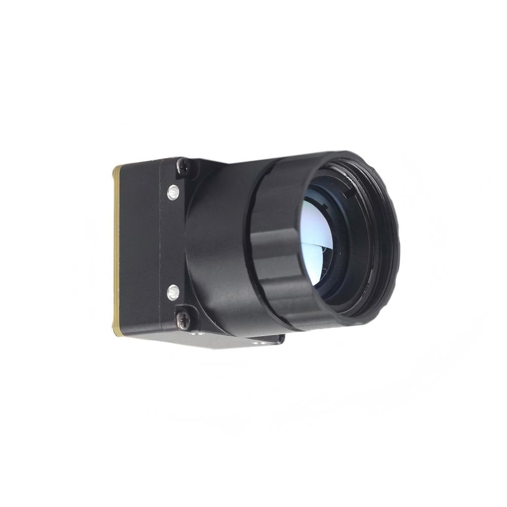
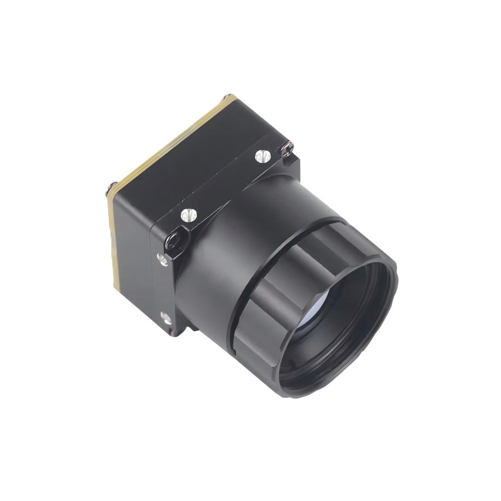
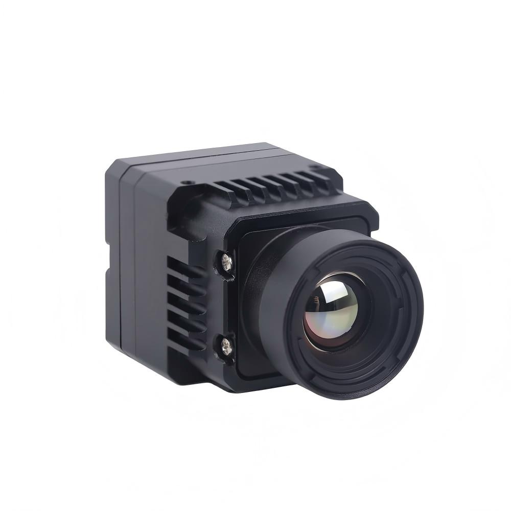
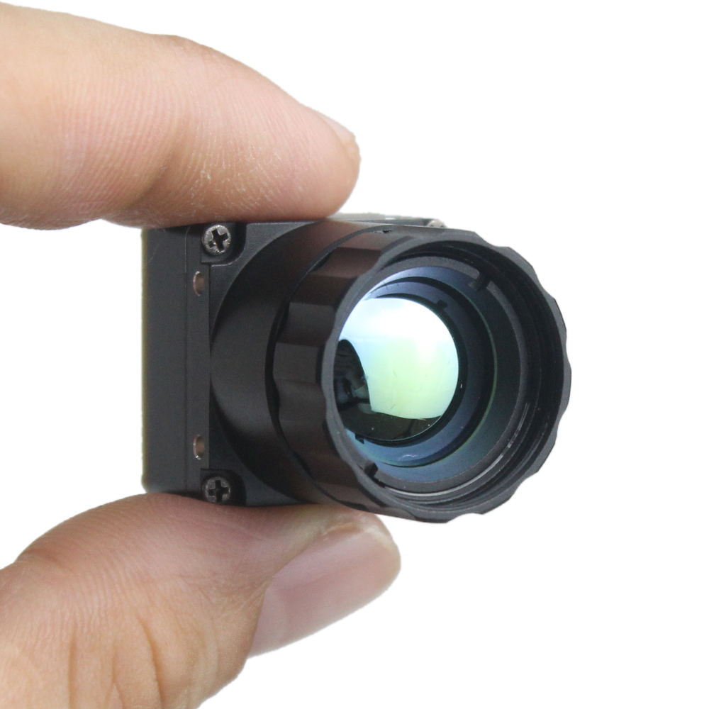
Purpleriver engineers and manufactures the MINI series of uncooled infrared camera modules, developed specifically to resolve SWaP-C challenges in airborne gimbals, tactical micro-drones, handheld test instrumentation, and embedded edge vision arrays.
Uncooled Infrared Mini2 640×512 9mm Thermal Imaging Camera Module For Drones
The Mini2 640×512 core represents our flagship high-resolution thermal imaging module designed for direct airborne deployment on drones and robotic platforms. Built around a sensitive 12 μm Vanadium Oxide (VOx) microbolometer array, the module delivers sharp, crisp image presentation, compact physical dimensions, and industry-leading cost-performance. Equipped with an integrated 9.0mm athermalized lens assembly and native MIPI CSI-2 interface, the Mini2 streams full 14-bit uncompressed digital raw temperature data alongside YUV display feeds, making it the ideal core for autonomous aerial surveillance, long-range thermal tracking, and search-and-rescue payloads.
- ✅ Array Format: 640 × 512 pixels (12 μm pixel pitch)
- ✅ Thermal Sensitivity: ≤ 40 mK (@25°C, F/1.0)
- ✅ Optical Configuration: 9.0 mm athermalized wide-FOV Germanium lens
- ✅ Interface: Native MIPI CSI-2 (Direct D-PHY), Low-profile FPC connectivity
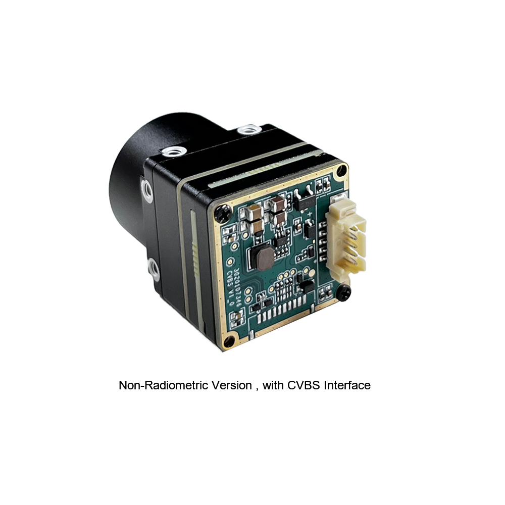
Uncooled Mini 384×288 Thermal Camera Module For Drones
The MINI 384×288 series infrared thermal imaging temperature measurement module is an ultra-compact, high-precision online radiometric imager. Utilizing high-stability microbolometer detectors, it balances high thermal resolution with minimal power draw. The module features extensive functional versatility and multiple interface configurations (MIPI CSI-2, CVBS, and digital expansion), making it the primary choice across machine vision, safety inspection, intelligent manufacturing, equipment maintenance, and lightweight robot/drone airborne platforms.
- ✅ Array Format: 384 × 288 pixels
- ✅ Radiometric Support: Precision point, line, and area online temperature measurement
- ✅ Multi-Interface Support: Direct MIPI CSI-2, Analog CVBS, and Industrial Expansion headers
- ✅ Application Scope: Industrial diagnostics, airborne pipeline inspection, automated optical inspection
Comprehensive Engineering Comparison Matrix
| Technical Parameter | Purpleriver Mini2 640×512 9mm | Purpleriver Mini 384×288 Series |
|---|---|---|
| Detector Architecture | Uncooled VOx (Vanadium Oxide) Microbolometer | High-Stability Uncooled Microbolometer |
| Focal Plane Array Resolution | 640 × 512 pixels | 384 × 288 pixels |
| Pixel Pitch | 12 μm | 12 μm / 17 μm options |
| Spectral Bandpass | 8 μm to 14 μm (LWIR) | 8 μm to 14 μm (LWIR) |
| Thermal Sensitivity (NETD) | ≤ 40 mK (@25°C, F/1.0) | ≤ 40 mK (@25°C, F/1.0) |
| Native Hardware Interface | MIPI CSI-2 (Direct D-PHY), Optional Parallel | MIPI CSI-2, Analog CVBS, Expansion I/O |
| Configurable Frame Rates | 25 Hz / 30 Hz / 50 Hz / 60 Hz | 25 Hz / 50 Hz / 60 Hz |
| Digital Output Pixel Formats | 14-bit RAW (Linear Radiometric), YUV422, YUV420 | 14-bit / 16-bit Radiometric Data, YUV/RGB Digital Out |
| Lens Options | 9.0 mm Athermalized Germanium Lens | Configurable Athermalized / Manual Focus Lenses |
| Temperature Measurement Modes | Full-frame radiometric online analysis | Point, line, area online high-precision radiometry |
| Supply Voltage & Consumption | DC 3.3V – 5.0V | < 800 mW | DC 3.3V – 5.0V | < 700 mW |
| Core Module Weight | < 20 grams (Excluding external bracket) | < 18 grams (Bare-board configuration) |
| Operating Temperature Range | -40°C to +80°C | -40°C to +70°C |
For procurement planning and detailed unit economics across custom development projects, refer to our comprehensive thermal camera module price guide 2024: from DIY kits to pro edge AI.
5. Radiometric Signal Processing: Non-Uniformity Correction (NUC) and Calibrated Telemetry
An uncalibrated microbolometer array cannot directly output true thermal imagery. Due to semiconductor manufacturing tolerances, individual microbolometer pixels exhibit variations in electrical resistance, temperature coefficients of resistance (TCR), and thermal dissipation characteristics. Without calibration, the raw output from a microbolometer array is dominated by fixed-pattern noise (FPN), obscuring the thermal scene.
Two-Point Non-Uniformity Correction (NUC) Physics
To convert spatial resistance offsets into a uniform image plane, Purpleriver MIPI cores implement real-time, hardware-accelerated Two-Point Non-Uniformity Correction:
Where:
- ⚙️
S_raw(i, j)represents the raw 14-bit ADC output count for pixel coordinates(i, j). - ⚙️
Offset(i, j)is the additive calibration matrix obtained during blackbody shutter calibration, compensating for differences in microbolometer thermal dissipation and substrate thermal gradients. - ⚙️
Gain(i, j)is the multiplicative responsivity correction matrix derived across wide-temperature calibration runs.
The thermal core balances two operational correction methods:
- ✅ Mechanical Shutter NUC: A solenoid drops an athermalized, uniform mechanical blade in front of the FPA for roughly 250 milliseconds. The module acquires uniform dark-field frames to refresh the offset matrix. This method provides the highest radiometric stability under rapid ambient temperature shifts.
- ✅ Shutterless Scene-Based NUC (SBNUC): For high-speed drone racing or tactical tracking where a shutter freeze is unacceptable, internal motion-estimation algorithms analyze inter-frame camera motion. High-frequency spatial fixed-pattern noise is isolated from dynamic low-frequency scene data, continuously updating the offset matrix without mechanical interruption.
Bad Pixel Replacement (BPR) Engine
Uncooled microbolometer yields inevitably include a small fraction of defective pixels—elements that remain stuck high (open circuit), stuck low (shorted), or display excessive 1/f flicker noise. During factory blackbody qualification, the thermal core generates an onboard defect table mapping these pixel coordinates into non-volatile flash. During real-time pipeline streaming, an 8-neighbor spatial median interpolation filter replaces dead pixels on the fly, preventing missing data points from destabilizing convolutional feature extractors in downstream AI layers.
Linear Kelvin Radiometric Conversion
When configured for radiometric data delivery over the MIPI CSI-2 bus, output pixel intensities map linearly to absolute target temperatures. Depending on the configured telemetry bit depth, each Least Significant Bit (LSB) corresponds to an exact Kelvin increment:
Under this scaling, a 14-bit digital count of 30,000 translates precisely to 300.00 Kelvin (+26.85°C). Purpleriver modules incorporate two selectable gain calibration states:
- ⚙️ High Gain Mode: Optimized for high sensitivity across environmental ranges (-20°C to +150°C). Noise Equivalent Temperature Difference (NETD) reaches ≤ 40 mK, resolving slight thermal variations across building envelopes, search-and-rescue scenes, or electrical wiring.
- ⚙️ Low Gain Mode: Compresses analog ROIC integration ramps to expand the dynamic range up to +550°C (or +650°C on custom configurations). This state is designed for industrial boiler monitoring, wildfire suppression, and localized smelting inspections.
6. Hardware Carrier Design: High-Speed Differential Routing and Connector Standards
Interfacing a native MIPI thermal camera module to custom embedded carrier boards requires rigorous high-speed layout practices. The MIPI D-PHY interface combines high-speed, sub-nanosecond edge-rate differential signaling (HS mode) with single-ended 1.2V signaling (LP mode). Improper routing leads to common-mode phase skew, signal reflection, packet corruption, and frame drops.
Differential Trace Geometry and Impedance Control
High-speed MIPI lines require strict impedance control across the PCB trace topology:
- ⚙️ Differential Impedance: All MIPI D-PHY differential clock pairs (
CLK_P,CLK_N) and data pairs (DATA0_P/N,DATA1_P/N) must be routed to achieve a target differential impedance of 100 Ω ± 10% (corresponding to a 50 Ω single-ended impedance to the reference ground). - ⚙️ Intra-Pair Length Skew: The absolute trace length delta between the positive (
_P) and negative (_N) traces of any single differential pair must not exceed 0.15 mm (6 mils). Skew imbalances convert differential signals into common-mode radiation, degrading EMI performance and distorting the eye diagram. - ⚙️ Inter-Pair Length Matching: The length difference between data lane pairs and the high-speed differential clock pair must remain within 1.0 mm (40 mils) to satisfy receiver setup-and-hold timing parameters.
- ⚙️ Continuous Reference Plane: High-speed pairs must run over an unbroken, solid copper Ground (GND) return plane. Never route MIPI traces across power plane splits or ground voids; discontinuities disrupt the return current path and induce significant jitter.
- ⚙️ Via Transitions: Signal vias should be minimized. Where layer transitions are necessary, route data lines through symmetrical via pairs flanked immediately by adjacent ground stitching vias placed within 0.5 mm to provide a continuous return path.
Interconnect Standards: Hirose Board-to-Board & FPC Headers
Purpleriver MINI series modules utilize specialized ultra-compact, multi-pin connectors—such as the high-speed mezzanine series from Hirose Electric (e.g., Hirose DF40 or DF12 low-profile families)—or locking micro-pitch Flexible Printed Circuit (FPC) headers.
| Pin Range | Signal Group | Signal Descriptions & Electrical Rules |
|---|---|---|
| 1, 4, 7, 10 | Digital GND | System ground return; isolates high-speed differential pairs to eliminate cross-talk. |
| 2, 3 | MIPI_CLK_N / P | Differential D-PHY DDR Clock Lane; requires 100 Ω differential trace routing. |
| 5, 6 | MIPI_DATA0_N / P | Differential High-Speed Data Lane 0; transmits packetized thermal byte streams. |
| 8, 9 | MIPI_DATA1_N / P | Differential High-Speed Data Lane 1; secondary data stream for 640×512 configurations. |
| 11, 12 | I2C_SDA / SCL | Control bus; requires 2.2 kΩ – 4.7 kΩ pull-up resistors to the 3.3V or 1.8V VDDIO rail. |
| 13, 14 | System Control | RESET_N (Active-low reset) and EXT_SYNC (Hardware genlock trigger for multi-spectral alignment). |
| 15, 16 | Core DC Power | Input supply rail (DC 3.3V to 5.0V); decouple locally with 0.1 μF and 10 μF ceramic capacitors. |
When routing flexible flat cables (FFC/FPC) across UAV 3-axis brushless gimbals, always select shielded flex designs featuring dual-sided solid silver or copper cross-hatch shielding. Gimbal motor commutations create localized electromagnetic fields; proper shielding prevents PWM switching transients from coupling into the high-speed differential D-PHY lines.
7. Frequently Asked Questions: Embedded Systems & Engineering Integration
How do I integrate a MIPI CSI-2 thermal camera module into embedded Linux platforms like Nvidia Jetson or Raspberry Pi?
Why should I choose native MIPI over USB 3.0 or CVBS for drone and robotic vision payloads?
Can Purpleriver MIPI thermal camera modules deliver accurate radiometric temperature data on custom carrier boards?
📚 References & Further Reading
- Industry Standard: Real-time image processing pipelines and zero-copy computer vision acceleration using the official OpenCV framework.
- Industry Standard: High-density micro-pitch board-to-board interconnect specifications by Hirose Electric.
- Related Guide: In-depth engineering walkthrough on high-performance thermal imaging module integration for edge AI & UAV OEM.
- Related Guide: Core sensor evaluation criteria in our AI thermal camera selection guide for high-precision OEM modules.
- Related Guide: Market architecture and budgetary tradeoffs in our thermal camera module price guide 2024: from DIY kits to pro edge AI.